
Properties of Al2O3 Thin Films Grown by PE-ALD at Low Temperature Using H2O and O2 Plasma Oxidants

 , , , , , , ,
Abstract
:1. Introduction
2. Materials and Methods
2.1. Thin Film Deposition
2.2. Thin Film Characterization
3. Results and Discussion
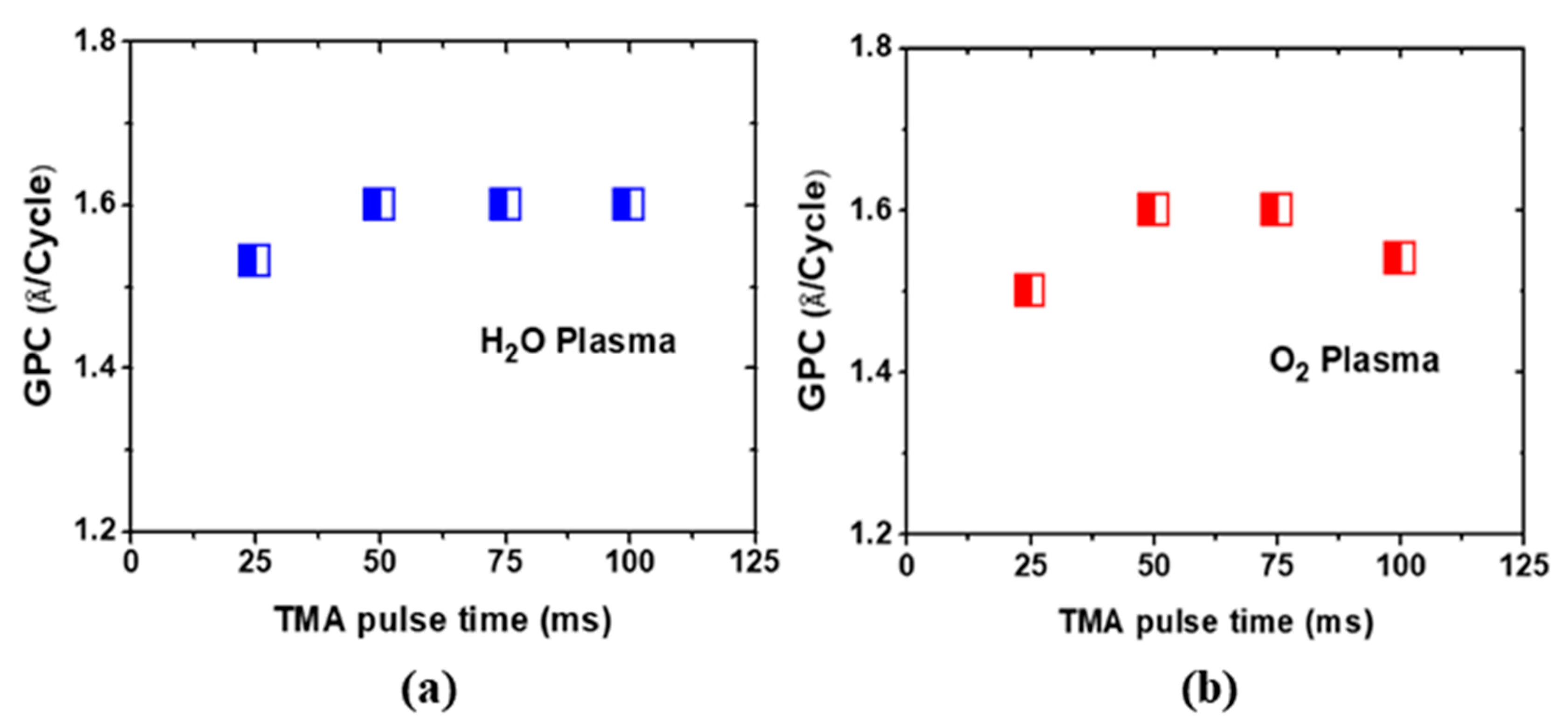
3.1. Thin Films Growth
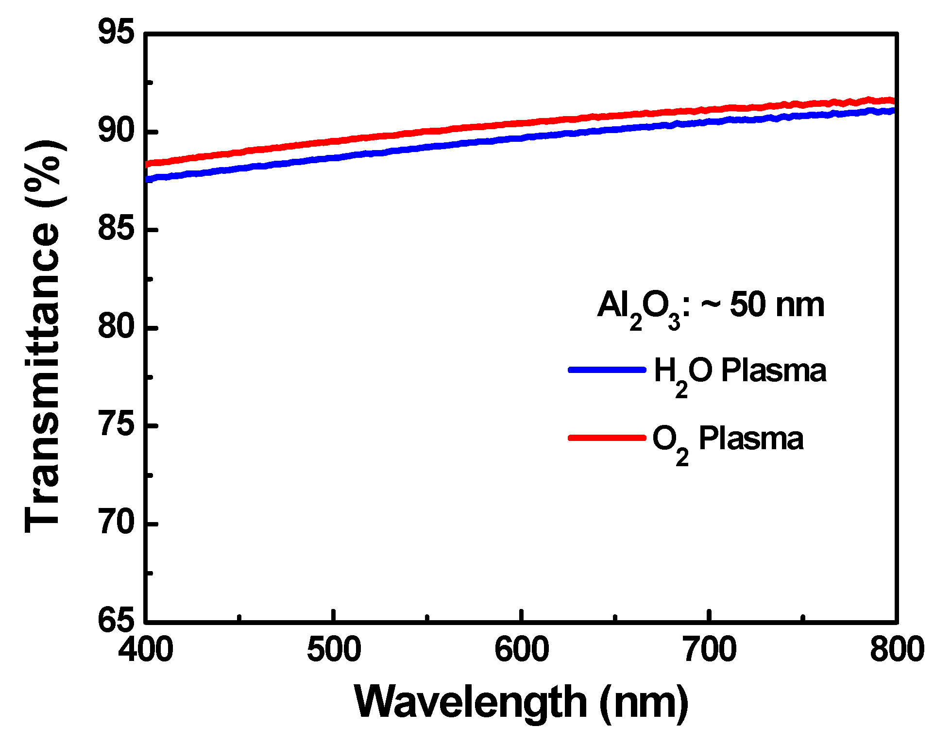
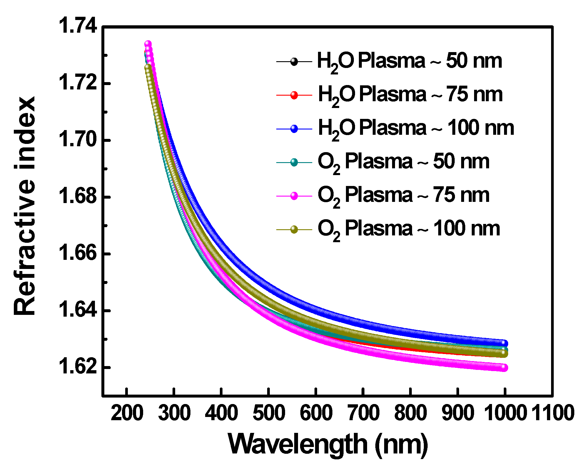
3.2. Optical Properties
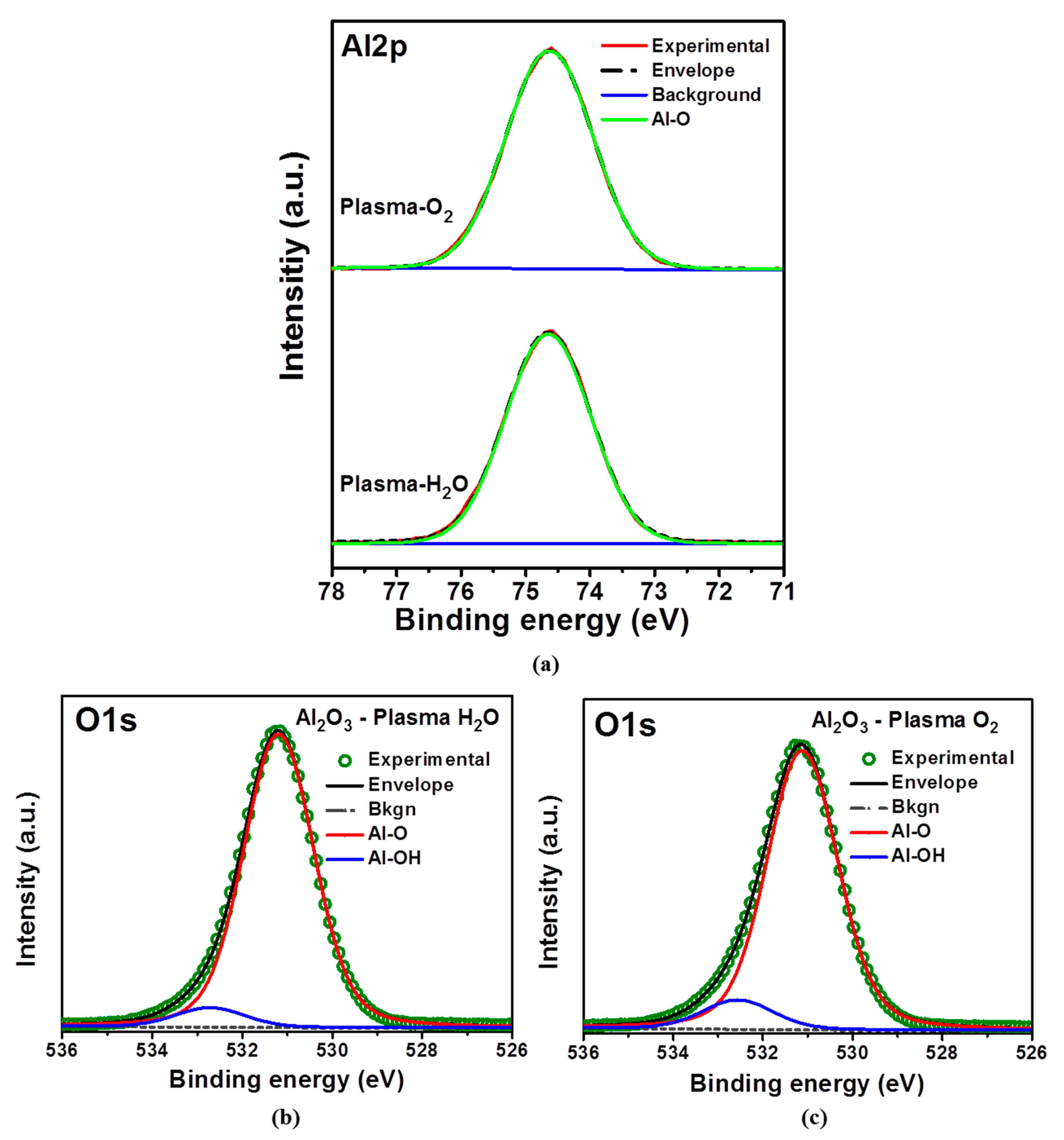
3.3. Compositional Analysis
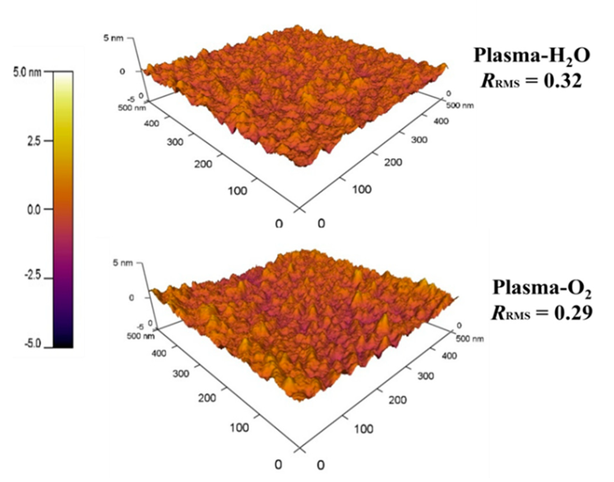
3.4. Morphological Properties
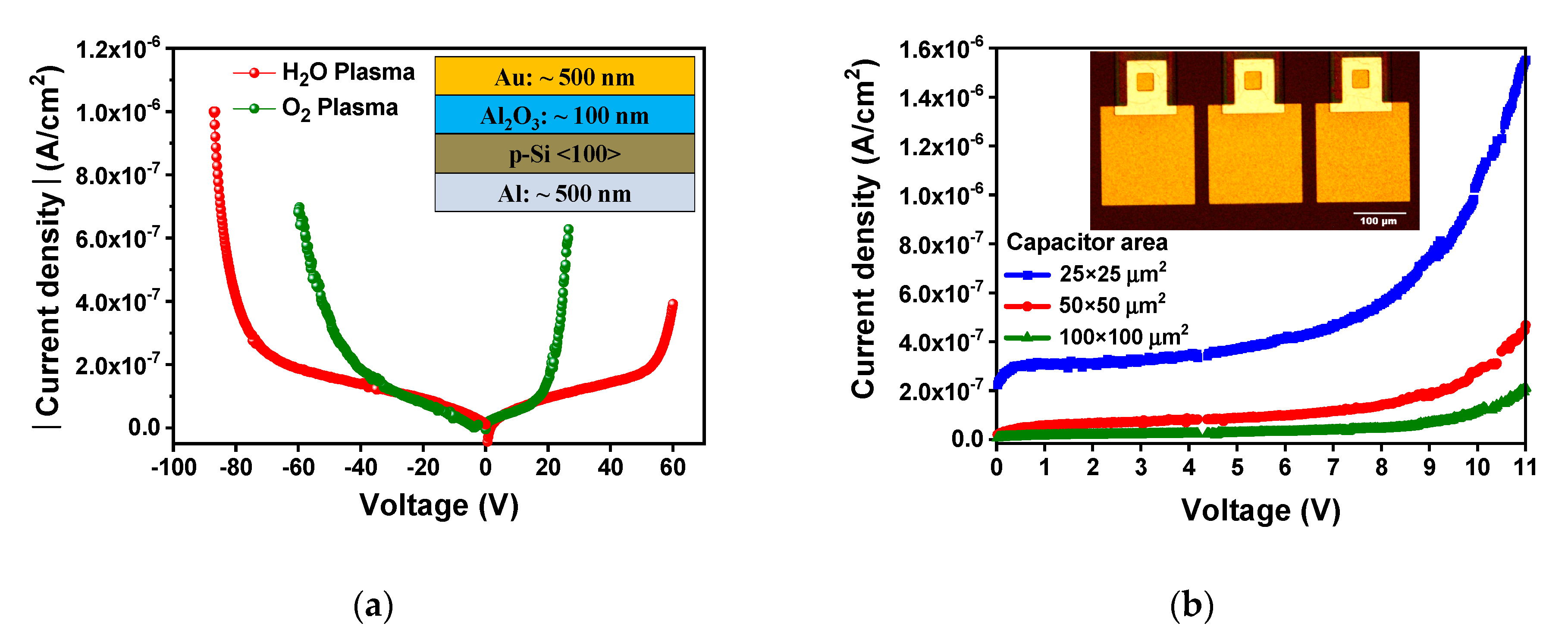
3.5. Electrical Characteristics
4. Conclusions
Author Contributions
Funding
Institutional Review Board Statement
Informed Consent Statement
Data Availability Statement
Acknowledgments
Conflicts of Interest
References
- Wang, B.; Huang, W.; Chi, L.; Al-Hashimi, M.; Marks, T.J.; Facchetti, A. High-k Gate Dielectrics for Emerging Flexible and Stretchable Electronics. Chem. Rev. 2018, 118, 5690–5754. [Google Scholar] [CrossRef]
- Gomes, T.C.; Kumar, D.; Fugikawa-Santos, L.; Alves, N.; Kettle, J. Optimization of the Anodization Processing for Aluminum Oxide Gate Dielectrics in ZnO Thin Film Transistors by Multivariate Analysis. ACS Comb. Sci. 2019, 21, 370–379. [Google Scholar] [CrossRef] [PubMed] [Green Version]
- Hoffmann, L.; Theirich, D.; Pack, S.; Kocak, F.; Schlamm, D.; Hasselmann, T.; Fahl, H.; Raupke, A.; Gargouri, H.; Riedl, T. Gas Diffusion Barriers Prepared by Spatial Atmospheric Pressure Plasma Enhanced ALD. ACS Appl. Mater. Interfaces 2017, 9, 4171–4176. [Google Scholar] [CrossRef] [PubMed]
- Choi, E.Y.; Kimb, J.; Limc, S.; Hana, E.; Ho-Baillie, A.W.Y.; Park, N. Enhancing stability for organic-inorganic perovskite solar cells by atomic layer deposited Al2O3 encapsulation. Sol. Energy Mater. Sol. Cells 2018, 188, 37–45. [Google Scholar] [CrossRef]
- Ha, J.W.; Ryu, H.; Lee, W.J.; Bae, J.S. Efficient photoelectrochemical water splitting using CuO nanorod/Al2O3 heterostructure photoelectrodes with different Al layer thicknesses. Phys. B 2017, 519, 95–101. [Google Scholar] [CrossRef]
- Fusco, M.A.; Oldham, C.J.; Parsons, G.N. Investigation of the Corrosion Behavior of Atomic Layer Deposited Al2O3/TiO2 Nanolaminate Thin Films on Copper in 0.1 M NaCl. Materials 2019, 12, 672. [Google Scholar] [CrossRef] [PubMed] [Green Version]
- Kotomin, E.A.; Kuzovkov, V.N.; Popov, A.I.; Vila, R. Kinetics of F center annealing and colloid formation in Al2O3. Nucl. Instrum. Methods Phys. Res. Sect. B Beam Interact. Mater. Atoms. 2016, 374, 107–110. [Google Scholar] [CrossRef]
- Zhou, G.; Wang, L.; Wang, X.; Yub, Y.; Mutzke, A. Effect of bias voltage on microstructure and optical properties of Al2O3 thin films prepared by twin targets reactive high power impulse magnetron sputtering. Vacuum 2019, 166, 88–96. [Google Scholar] [CrossRef]
- Balakrishnana, G.; Sundari, S.T.; Ramaseshan, R.; Thirumurugesan, R.; Mohandas, E.; Sastikumar, D.; Kuppusami, P.; Kim, T.G.; Song, J.I. Effect of substrate temperature on microstructure and optical properties of nanocrystalline alumina thin films. Ceram. Int. 2013, 39, 9017–9023. [Google Scholar] [CrossRef]
- Kumar, V.S.R.S.P.; Kumar, M.; Kumari, N.; Sharma, A.L. Optical and morphological studies of aluminium oxide films fabricated at different leaning angles using ion assisted E-Beam deposition technique. Opt.—Int. J. Light Electron Opt. 2020, 222, 165376. [Google Scholar] [CrossRef]
- Jo, J.-W.; Kim, K.-H.; Kim, J.; Ban, S.G.; Kim, Y.-H.; Park, S.K. High-Mobility and Hysteresis-Free Flexible Oxide Thin-Film Transistors and Circuits by Using Bilayer Sol−Gel Gate Dielectrics. ACS Appl. Mater. Interfaces 2018, 10, 2679–2687. [Google Scholar] [CrossRef] [PubMed]
- Kumar, P.; Wiedmann, M.K.; Winter, C.H.; Avrutsky, I. Optical properties of Al2O3 thin films grown by atomic layer deposition. Appl. Opt. 2009, 48, 5407–5412. [Google Scholar] [CrossRef] [PubMed]
- Barbos, C.; Blanc-Pelissier, D.; Fave, A.; Botella, C.; Regreny, P.; Grenet, G.; Blanquet, E.; Crisci, A.; Lemiti, M. Al2O3 thin films deposited by thermal atomic layer deposition: Characterization for photovoltaic applications. Thin Solid Films 2016, 617, 108–113. [Google Scholar] [CrossRef] [Green Version]
- Schmidt, J.; Merkle, A.; Brendel, R.; Hoex, B.; van de Sanden, M.C.M.; Kessels, W.M.M. Research Surface Passivation of High-efficiency Silicon Solar Cells by Atomic-layer-deposited Al2O3. Prog. Photovolt. Res. Appl. 2008, 16, 16461–16466. [Google Scholar] [CrossRef]
- Profijt, H.B.; Potts, S.E.; van de Sanden, M.C.M.; Kessels, W.M.M. Plasma-Assisted Atomic Layer Deposition: Basics, Opportunities, and Challenges. J. Vac. Sci. Technol. A 2011, 29, 050801. [Google Scholar] [CrossRef] [Green Version]
- Castillo, M.A.L.; Toledo-Guizar, P.G.; Adame, J.A.A.; Garcia, R.; Cuevas, F.J.H.; Aleman, M.; Hernandez-Como, N. Decreasing the Vth shift of InGaZnO thin-film transistors under positive and negative bias stress using SU-8 as etch-stop and passivation layer. Semicond. Sci. Technol. 2020, 35, 125024. [Google Scholar] [CrossRef]
- Hiraiwa, A.; Matsumura, D.; Kawarada, H. Effect of atomic layer deposition temperature on current conduction in Al2O3 films formed using H2O oxidant. J. Appl. Phys. 2016, 120, 084504. [Google Scholar] [CrossRef]
- Gieraltowska, S.; Wachnicki, L.; Witkowski, B.S.; Mroczynski, R.; Dluzewski, P.; Godlewski, M. Characterization of dielectric layers grown at low temperature by atomic layer deposition. Thin Solid Films 2015, 577, 97–102. [Google Scholar] [CrossRef]
- Ali, K.; Choi, K.-H. Low-Temperature Roll-to-Roll Atmospheric Atomic Layer Deposition of Al2O3 Thin Films. Langmuir 2014, 30, 14195–14203. [Google Scholar] [CrossRef]
- Choi, K.-H.; Ali, K.; Kim, C.Y.; Muhammad, N.M. Characterization of Al2O3 Thin Films Fabricated at Low Temperature via Atomic Layer Deposition on PEN Substrates. Chem. Vap. Depos. 2014, 20, 118–124. [Google Scholar] [CrossRef]
- Yang, Y.-Q.; Duan, Y.; Chen, P.; Sun, F.-B.; Duan, Y.-H.; Wang, X.; Yang, D. Realization of Thin Film Encapsulation by Atomic Layer Deposition of Al2O3 at Low Temperature. J. Phys. Chem. C 2013, 117, 20308–20312. [Google Scholar] [CrossRef]
- Zhu, Z.; Sippola, P.; Lipsanen, H.; Savin, H.; Merdes, S. Influence of plasma parameters on the properties of ultrathin Al2O3 films prepared by plasma enhanced atomic layer deposition below 100 °C for moisture barrier applications. Jpn. J. Appl. Phys. 2018, 57, 125502. [Google Scholar] [CrossRef] [Green Version]
- Lale, A.; Joly, M.; Mekkaoui, S.; Joly, X.; Scheid, E.; Launay, J. Pierre Temple-Boyer, Effect of thermal annealing on the dielectric, passivation and pH detection properties of aluminium oxide thin films deposited by plasma-enhanced atomic layer deposition. Thin Solid Films 2021, 735, 138761. [Google Scholar] [CrossRef]
- Schilirò, E.; Fiorenza, P.; Greco, G.; Roccaforte, F.; Nigro, R.L. Plasma enhanced atomic layer deposition of Al2O3 gate dielectric thin films on AlGaN/GaN substrates: The role of surface predeposition treatments. J. Vac. Sci. Technol. A 2017, 35, 01B140. [Google Scholar] [CrossRef]
- Zhu, Z.; Merdes, S.; Ylivaara, O.M.E.; Mizohata, K.; Heikkilä, M.J.; Savin, H. Al2O3 Thin Films Prepared by a Combined Thermal-Plasma Atomic Layer Deposition Process at Low Temperature for Encapsulation Applications. Phys. Status Solidi A 2020, 217, 1900237. [Google Scholar] [CrossRef]
- Haeberle, J.; Henkel, K.; Gargouri, H.; Naumann, F.; Gruska, B.; Arens, M.; Tallarida, M.; Schmeißer, D. Ellipsometry and XPS comparative studies of thermal and plasma enhanced atomic layer deposited Al2O3-films. Beilstein J. Nanotechnol. 2013, 4, 732–742. [Google Scholar] [CrossRef] [Green Version]
- Aslan, M.M.; Webster, N.A.; Byard, C.L.; Pereira, M.B.; Hayes, C.M.; Wiederkehr, R.S.; Mendes, S.B. Low-loss optical waveguides for the near ultra-violet and visible spectral regions with Al2O3 thin films from atomic layer deposition. Thin Solid Films 2010, 518, 4935–4940. [Google Scholar] [CrossRef] [PubMed] [Green Version]
- Kim, H.G.; Kim, S.S. Aluminum oxide barrier coating on polyethersulfone substrate by atomic layer deposition for barrier property enhancement. Thin Solid Films 2011, 520, 481–485. [Google Scholar] [CrossRef]
- Houska, J.; Blazek, J.; Rezek, J.; Proksova, S. Overview of optical properties of Al2O3 films prepared by various techniques. Thin Solid Films 2012, 520, 5405–5408. [Google Scholar] [CrossRef]
- Iatsunskyi, I.; Kempinski, M.; Jancelewicz, M.; Załeski, K.; Jurga, S.; Smyntyna, V. Structural and XPS characterization of ALD Al2O3 coated porous silicon. Vacuum 2015, 113, 52–58. [Google Scholar] [CrossRef]
- Singh, S.D.; Nand, M.; Das, A.; Ajimsha, R.S.; Upadhyay, A.; Kamparath, R.; Shukla, D.K.; Mukherjee, C.; Misra, P.; Rai, S.K.; et al. Structural, electronic structure, and band alignment properties at epitaxial NiO/Al2O3 heterojunction evaluated from synchrotron based X-ray techniques. J. Appl. Phys. 2016, 119, 165302. [Google Scholar] [CrossRef]
- Tahir, D.; Kwon, H.L.; Shin, H.C.; Oh, S.K.; Kang, H.J.; Heo, S.; Chung, J.G.; Lee, J.C.; Tougaard, S. Electronic and optical properties of Al2O3/SiO2 thin films grown on Si substrate. J. Phys. D Appl. Phys. 2010, 43, 255301. [Google Scholar] [CrossRef] [Green Version]
- Nichols, M.T.; Li, W.; Pei, D.; Antonelli, G.A.; Lin, Q.; Banna, S.; Nishi, Y.; Shohet, J.L. Measurement of bandgap energies in low-k organosilicates. J. Appl. Phys. 2014, 115, 094105. [Google Scholar] [CrossRef] [Green Version]
- Hudait, M.K.; Zhu, Y. Energy band alignment of atomic layer deposited HfO2 oxide film on epitaxial (100)Ge, (110)Ge, and (111)Ge layers. J. Appl. Phys. 2013, 113, 114303. [Google Scholar] [CrossRef] [Green Version]
- Lu, H.L.; Yang, M.; Xie, Z.Y.; Geng, Y.; Zhang, Y.; Wang, P.F.; Sun, Q.Q.; Ding, S.J.; Zhang, D.W. Band alignment and interfacial structure of ZnO/Si heterojunction with Al2O3 and HfO2 as interlayers. Appl. Phys. Lett. 2014, 104, 161602. [Google Scholar] [CrossRef]
- Afanas’ev, V.V.; Houssa, M.; Stesmans, A.; Merckling, C.; Schram, T.; Kittl, J.A. Influence of Al2O3 crystallization on band offsets at interfaces with Si and TiNx. Appl. Phys. Lett. 2011, 99, 072103. [Google Scholar] [CrossRef]
- Rahman, M.; Shin, K.Y.; Kim, T.W. Characterization of Electrical Traps Formed in Al2O3 under Various ALD Conditions. Materials 2020, 13, 5809. [Google Scholar] [CrossRef] [PubMed]
- Rahman, M.M.; Kim, J.-G.; Kim, D.-H.; Kim, T.-W. Border Trap Extraction with Capacitance- Equivalent Thickness to Refect the Quantum Mechanical Efect on Atomic Layer Deposition High-k/In0.53Ga0.47As on 300-mm Si Substrate. Sci. Rep. 2019, 9, 9861. [Google Scholar] [CrossRef] [Green Version]
- Kim, Y.; Kwon, H.; Han, H.S.; Kim, H.K.; Kim, B.S.Y.; Lee, B.C.; Lee, J.; Asheghi, M.; Prinz, F.B.; Goodson, K.E.; et al. Tunable Dielectric and Thermal Properties of Oxide Dielectrics via Substrate Biasing in Plasma Enhanced Atomic Layer Deposition. ACS Appl. Mater. Interfaces 2020, 12, 44912–44918. [Google Scholar] [CrossRef]


| Sample | Cycles | GPC (Å/Cycle) | Thickness (nm) |
|---|---|---|---|
| H2O Plasma | 300 | ~1.7 | 50 |
| 470 | ~1.7 | 80 | |
| 650 | ~1.7 | 110 | |
| O2 Plasma | 300 | ~1.6 | 50 |
| 470 | ~1.6 | 75 | |
| 680 | ~1.6 | 100 |
| Sample | Thickness (nm) | MSE | n (at λ = 632.8 nm) |
|---|---|---|---|
| H2O-Plasma ~50 nm H2O-Plasma ~75 nm H2O-Plasma ~100 nm O2-Plasma ~50 nm O2-Plasma ~75 nm O2-Plasma ~100 nm | 59.8 89.7 120.6 52.0 81.5 112.4 | 4.9 3.7 3.9 3.2 3.4 4.1 | 1.63 1.63 1.64 1.63 1.63 1.63 |
| Techniques | Thickness (nm) | n | Year/Ref |
|---|---|---|---|
| ALD | 200–400 | 1.64 | 2009/[12] |
| ALD | 210–380 | 1.64 | 2010/[27] |
| PE-ALD | 10–50 | 1.62–1.66 | 2011/[28] |
| HIPIMS | 240–1030 | 1.59–1.77 | 2012/[29] |
| Pulsed sputtering | 1140–1960 | 1.65–1.66 | |
| Annealing of Al | 300–350 | 1.66–1.67 | |
| ALD | 50 | 1.64 | 2013/[26] |
| ALD | 50–100 | 1.65 | 2016/[13] |
| PE-ALD | 50–100 | 1.63–1.64 | This work |
| Sample | Total O/Al | OAl-O/AlAl-O | OH/Al |
|---|---|---|---|
| H2O plasma O2 plasma | 1.48 1.50 | 1.39 1.36 | 0.09 0.14 |
| Capacitor Area | Dielectric Thickness | Capacitance (pF) | Dielectric Constant (κ) |
|---|---|---|---|
| 25 × 25 μm2 50 × 50 μm2 100 × 100 μm2 | 25 nm | 1.69 5.77 22.3 | 7.6 6.5 6.3 |
| Tech. | T (°C) | Oxidant Agent | TMA Time (s) | GPC (Å/Cycle) | Growth Rate Per Second (Å/s) | Dielectric Thickness (nm) | Dielectric Constant (κ) | Breakdown Electric Field (MV/cm) | Year/Ref. |
|---|---|---|---|---|---|---|---|---|---|
| PEALD | 300 | O2 | 0.025 | ~0.94 | ~5.2 × 10⁻² | ~37.5 | 8.6 | - | 2021 [23] |
| PEALD-ALD | 90 | O2/H2O | 0.2 | 0.84–1.28 | - | - | - | - | 2020 [25] |
| PEALD | 250 | O2 | 0.25 | ~1.37 | ~6.8 × 10⁻² | ~40 | 9 ± 1 | - | 2020 [39] |
| ALD | 200–300 | H2O | 0.1 | - | - | 3.5–4.2 | 6.2–6.9 | 4.7–6.5 | 2020 [37] |
| ALD | 200–300 | H2O | 0.1 | - | - | 3.5–4.2 | 6.2–6.9 | - | 2019 [38] |
| PEALD | 90 | O2 | 0.2 | 1.07–1.57 | - | ~4 | - | - | 2018 [22] |
| PEALD | 250 | O2 | 0.06 | ~1.1 | ~3.6 × 10⁻² | 27–28 | 5–6.1 | - | 2017 [24] |
| ALD | 100–450 | H2O | - | 0.73–0.98 | - | 33–44 | 7–9 | 2–4 | 2016 [17] |
| ALD | 85 | H2O | - | 0.80 | ~4.0 × 10⁻² | 20 | 10 ± 3 | ~2.5 | 2015 [18] |
| AALD | 25–50 | H2O | - | 0.62–0.97 | - | 20 | - | 0.75–1.8 | 2014 [19] |
| ALD | 35 | H2O | 2 | 1.14 | - | 19 | - | - | 2014 [20] |
| ALD | 80 | H2O and O3 | - | 0.90–0.95 | - | 60 | - | ~1.3 | 2013 [21] |
| PEALD | 70 | H2O | 0.05 | ~1.7 | ~7.8 × 10⁻² | ~25 | 6.3–7.6 | 4.8–5 | This work |
Publisher’s Note: MDPI stays neutral with regard to jurisdictional claims in published maps and institutional affiliations. |
© 2021 by the authors. Licensee MDPI, Basel, Switzerland. This article is an open access article distributed under the terms and conditions of the Creative Commons Attribution (CC BY) license (https://creativecommons.org/licenses/by/4.0/).
Share and Cite
Castillo-Saenz, J.; Nedev, N.; Valdez-Salas, B.; Curiel-Alvarez, M.; Mendivil-Palma, M.I.; Hernandez-Como, N.; Martinez-Puente, M.; Mateos, D.; Perez-Landeros, O.; Martinez-Guerra, E. Properties of Al2O3 Thin Films Grown by PE-ALD at Low Temperature Using H2O and O2 Plasma Oxidants. Coatings 2021, 11, 1266. https://doi.org/10.3390/coatings11101266
Castillo-Saenz J, Nedev N, Valdez-Salas B, Curiel-Alvarez M, Mendivil-Palma MI, Hernandez-Como N, Martinez-Puente M, Mateos D, Perez-Landeros O, Martinez-Guerra E. Properties of Al2O3 Thin Films Grown by PE-ALD at Low Temperature Using H2O and O2 Plasma Oxidants. Coatings. 2021; 11(10):1266. https://doi.org/10.3390/coatings11101266
Chicago/Turabian StyleCastillo-Saenz, Jhonathan, Nicola Nedev, Benjamín Valdez-Salas, Mario Curiel-Alvarez, María Isabel Mendivil-Palma, Norberto Hernandez-Como, Marcelo Martinez-Puente, David Mateos, Oscar Perez-Landeros, and Eduardo Martinez-Guerra. 2021. "Properties of Al2O3 Thin Films Grown by PE-ALD at Low Temperature Using H2O and O2 Plasma Oxidants" Coatings 11, no. 10: 1266. https://doi.org/10.3390/coatings11101266
APA StyleCastillo-Saenz, J., Nedev, N., Valdez-Salas, B., Curiel-Alvarez, M., Mendivil-Palma, M. I., Hernandez-Como, N., Martinez-Puente, M., Mateos, D., Perez-Landeros, O., & Martinez-Guerra, E. (2021). Properties of Al2O3 Thin Films Grown by PE-ALD at Low Temperature Using H2O and O2 Plasma Oxidants. Coatings, 11(10), 1266. https://doi.org/10.3390/coatings11101266