1. Introduction
Gallium nitride (GaN) is a versatile semiconductors material with wide direct band gap, good thermal conductivity, high breakdown voltage, and high electron mobility [
1]. GaN and its alloys have been employed for light-emitting diodes and laser diodes [
2,
3], field effect transistors, and hetero-junction bipolar transistors [
4,
5]. GaN films have been grown by many fabrication methods, including metal-organic chemical vapor deposition (MOCVD), metal-organic vapor phase epitaxy (MOVPE), and molecular beam epitaxy (MBE) [
6,
7,
8].
To further develop the electronic and optoelectronic properties, it is advantageous to control the growth of GaN film so that it is
p-type hole conduction by controlling acceptor concentration. In 1989, H. Amano et al. studied Mg-doped GaN films by low-energy electron beam irradiation (LEEBI) treatment and their films converted into a
p-type semiconductor with low resistivity of 35 Ω·cm, hole concentration of 2 × 10
16 cm
−3, and electrical mobility of 8 cm
2·V
−1·s
−1 [
9]. In 1991, S. Nakamura developed a two-flow (TF) MOCVD to grow GaN with significantly improved crystallinity, uniformity, and electrical properties [
10]. In 1992, S. Nakamura et al. achieved low resistivity
p-type GaN film grown by TF-MOCVD at temperature above 700 °C under a N
2 atmosphere. The resistivity of the Mg-GaN film remarkably decreased to 2 Ω·cm, with a hole concentration of 3 × 10
17 cm
−3 and electrical mobility of 10 cm
2·V
−1·s
−1 [
11]. In 1998, C.G. Van de Walle showed that there was a limit in the hole concentration of
p-type GaN due to the solubility of Mg in GaN [
12]. In 2010, C. Guarneros et al. had successfully grown GaN and Mg-GaN films on sapphire substrates with MOCVD, and investigated the optical and electrical properties of
n-GaN and
p-GaN films [
13]. They enhanced the electrical characteristics of
p-MgGaN films by annealing, resulting in a higher hole concentration of 4.82 × 10
19 cm
−3, lower resistivity of 7 × 10
−3 Ω·cm, and higher mobility of 18.4 cm
2·V
−1·s
−1. In 1995, S. Fischer group studied Zn dopant as acceptors in GaN and reported the blue light-emitting characteristic of Zn-doped GaN. After being compared with Mg-doped GaN, Zn-GaN showed higher activation energy. [
14]. In 1988, H. Amano et al. used the MOVPE method to deposit a ~50 nm AlN buffer layer on
a- and
c-axis sapphire substrates at 950 °C, following the deposition of 0.3 µm-thick Zn-GaN film with trimethylgallium (TMG), ammonia (NH
3), and Ethyl zinc (DEZ) as the sources of Ga, N, and Zn, respectively. The Zn-GaN film had good quality with no presence of cracks [
15]. In 2014, our group successfully deposited Mg-doped GaN films on Si (100) substrates at and below 400 °C by radio frequency reactive sputtering technology. At 10.2% Mg, Mg-GaN converted into a p-type semiconductor with hole concentration of 9.37 × 10
16 cm
−3, high electrical mobility of 345 cm
2·V
−1·s
−1, and high conductivity of 3.23 S·cm
−1 [
16].
Many reports have recently detailed the structural, optical, and electrical behaviors of GaN-Sb alloys grown as highly mismatched alloys (HMAs). However, the synthesis of HMAs is difficult due to the large size/electronegativity mismatch between anions of N and Sb, and unconventionally low growth temperature to be utilized for Sb incorporation. The most common growth method for GaN
1−xSb
x has been molecular beam epitaxy. Segercrantz el al. reported the optical characteristics of GaN
1−xSb
x films formed with Sb shutter to have Sb content of
x at 0.03–0.42. GaN
1−xSb
x films with Sb compositions less than 20% are of interest for photo-electrochemical (PEC) applications [
17]. In 2016, N. Segercrantz further presented the influences of rapid thermal annealing on the structural and electronic properties of GaN
1−xSb
x films with
x ≥ 0.06 grown by MBE at low temperature. P-type GaN
1−xSb
x semiconductor films were measured to have higher hole concentrations of ~10
19 cm
−3 after annealing at 400 °C [
18]. K. M. Yu also studied GaN
1−xSb
x grown on sapphire substrate by MBE at low temperature. They found that the growth temperature affected the Sb incorporation and the resulting structural and optical properties of GaN
1−xSb
x films [
19]. By using the low temperature MBE for the deposition of GaN-Sb films, K. M. Yu further investigated the structural and optical properties of N-rich GaN
1−xSb
x thin films [
20]. These N-rich GaN
1−xSb
x films with less than 5 at.% Sb had a bandgap of ~2 eV, which is suitable for PEC application. By using both positron annihilation measurement and ab initio calculation, N. Segercrantz discussed the possible reasons for the enhanced conductivity of the
p-type GaN
xSb
1−x films grown by plasma-assisted MBE [
21]. The GaN
xSb
1−x film is interesting and has demonstrated special properties, but all the GaNSb made by MBE had the Sb incorporated at the N anion site to behave as Sb
3−. In 2016, K. M. Yu studied and reported the composition range, the electronic band, and optical properties of highly mismatched GaN
1−xSb
xalloys [
22].
At present, there are few studies for the deposition of Sb-added GaN thin films by reactive radio frequency (RF) sputtering technology, which has beneficial characteristics such as relative low-cost, easy cleaning, low working temperature, and safety in the working environment. By using single ceramic target made with multiple components to get rid of troubles in utilizing liquid Ga target, our group has effectively used radio frequency reactive sputtering technology for III-nitride alloys. Due to the composition design of targets over a wide range, the different doping studies in GaN and its alloys have been quite successfully demonstrated [
23,
24,
25,
26]. With a systematic modification in the film composition, the effect of the Sb dopant on the solid solubility, the topology, and properties of Sb-GaN films can be studied and understood for the sake of its development on the emerging field. For scientific interests, Sb-doped GaN thin films with different Sb contents on Si (100) wafer are deposited by RF reactive sputtering technology with single cermet antimony-containing targets in this work. The properties of Sb-
x-GaN films and the performance of fabricated diode device on
n-Si are investigated.
2. Experimental Details
The deposition of Sb-x-GaN films on both SiO2/n-type Si (100) and n-type Si (100) substrates, with electrical resistivity of ~1–10 Ω·cm, electron concentration of ~1015·cm−3, diameter of 2 inches, thickness of ~550 μm and electrical mobility of ~200 cm2·V−1·s−1, was grown by radio frequency reactive sputtering with single cermet targets of various Sb dopants. Five Sb-x-GaN targets with x of the Sb/(Sb+Ga) molar ratios at 0, 0.04, 0.07, 0.14, and 0.2 were used for the deposition and labeled as Sb-x-GaN film with x = 0, 0.04, 0.07, 0.14, and 0.2. The SbGaN cermet targets consisting of different Sb contents were formed by hot-pressing the mixing powders of GaN ceramic and metallic Sb and Ga in accordance with composition design. To remove the oxygen and impurities present in deposition chamber, mechanical and diffusion pumps had been applied to vent the chamber to pressure lower than 1 × 10⁻⁶ torr before sputtering. As the influences of RF sputtering power and heating temperature on properties of doped GaN films had been well studied in our previous works, the RF sputtering power and substrate temperature in this work were set in 120 W and 300 °C, respectively, with the deposition pressure kept at 9 × 10⁻³ torr for 30 min and the mixing (Ar + N2) gas flow rates at 5 sccm and 15 sccm, respectively. A larger amount of N2 gas rate was used in the deposition to avoid nitrogen deficiency in GaN. The size of the single cermet target employed in RF sputtering was 5.08 cm (2 inches) and the work distance between Sb-containing target and substrates in the deposition chamber was kept at 5 cm.
By employing RF reactive sputtering technology, the hetero-junction diodes have been also fabricated by depositing Sb-
x-GaN thin films on
n-Si (100) wafers. The diode structure was in the top-top electrode mode formed by sputtering the p-SbGaN film on n-Si substrate shown in
Figure 1a. As known in the modeling of MOS, MS, homo or hetero junction diode, and metals with high work-function (Pt, Mo, Ni, …) were often used to make Schottky contact with
n-type semiconductor and Ohmic contact with
p-type semiconductor. On the other hand, metals with low work-function (Al, Ag, …) were often used to make ohmic contact with n-type semiconductor and Schottky contact with p-type semiconductor. Modeling of Pt/
p-Sb-GaN/
n-Si/Al in this work used Al to form ohmic contact with
n-Si and Pt to form Ohmic contact with
p-Sb-GaN.
Figure 1b,c presented the I-V characteristics of Al/
n-Si(100)/Al and Pt/
p-SbGaN/Pt Ohmic contacts, respectively. The diodes with hetero-junction were fabricated by depositing the
p-type Sb-0.07-GaN, Sb-0.14-GaN, and Sb-0.2-GaN films on
n-Si substrates. The commercial Al and Pt targets (99.999%) were used to deposit the electrodes at 200 °C for 30 min on the top of film. The physical processes for fabricating the diodes with our deposited III-nitride thin films were detailed in our previous works [
16,
25,
27,
28,
29].
X-ray photoelectron spectroscopy (XPS) measurements of films were obtained with VG scientific ESCALAB 250 (Billerica, MA, USA) spectrometer under Al Kα X-rays (hν = 1486.6 eV) radiation. The results were calibrated with carbon (C1s) binding energy. X-ray diffractometry (XRD, D8 Discover, Bruker, Billerica, MA, USA) and high-resolution transmission electron microscopy (HRTEM, Technai G2, Philips, WI, USA) were used to investigate the structural properties of the of Sb-x-GaN films. Atomic force microscopy (AFM, Dimension Icon, Bruker, Billerica, MA, USA) was used to assess the surface properties. The surface morphology, cross-sections, and EDS compositional data of Sb-x-GaN films were studied by scanning electron microscopy (SEM, JSM–6500F, JEOL, Tokyo, Japan) with energy dispersive spectrometry (EDS, JSM–6500F, JEOL, Tokyo, Japan). The absorption spectra for Sb-doped GaN thin films were obtained by ultraviolet-visible (UV-vis) spectrometry (V-670, Jasco, Tokyo, Japan). The electrical properties were investigated by Hall measurements (HMS-2000, Ecopia, Tokyo, Japan) with a maximum magnetic field of 0.51 T. The values of EDS composition analyses, the film thickness, surface roughness, electrical mobility, concentration and conductivity of the Sb-x-GaN samples were measured and calculated with the standard deviation (SD) at 5%. The electrical behaviors of the diodes were examined with I-V curves obtained with a Semiconductor Device Analyzer (Agilent, B1500A, Santa Crala, CA, USA) at RT.
3. Results and Discussion
Figure 2 shows (a) XPS survey scan and high resolution, (b) Ga 2p, (c) Sb 3d, and (d) N 1s spectra of the Sb-0.14-GaN film. XPS was used to determine the chemical surface properties of the Sb-0.14-GaN film deposited on
n-Si (100) wafer doped with phosphorus. The XPS survey data and the XPS peaks of Ga, Sb, and N elements shown in
Figure 1 were investigated with the low intensity peak of C 1s at 284.6 eV in binding energy as a reference.
Figure 2b shows the high resolution XPS spectrum with strong Ga 2p1/2 and Ga 2p3/2 peaks at 1145.7 eV and 1118.81 eV, respectively, for the confirmation of Ga-N bond in GaN [
30]. The small peak at 1117.8 eV was contributed to the Ga-O bonding.
Figure 2c shows the high resolution XPS peaks of Sb 3d3/2 and Sb 3d5/2 located at 540.2 eV and 530.98 eV, respectively, for Sb
3+ in SbN bond [
31], while peaks at 358.4 eV and 529.15 eV in binding energy were determined for Sb
3− in GaSb bond [
32,
33].
From the areal analysis of XPS fitting peak for Sb-0.14-GaN film, the ratio of Sb
3+ in Sb-N was 73.3% and the ratio of Sb
3− in Sb-Ga was 26.7%. The Sb substitution in GaN has Sb mainly to the cation site of Ga and some to the anion site of N. It can be the first observation to simultaneously show Sb in the valency states of 3+ and 3−. In the Sb 3d5/2 peak, there is the O 1s peak overlapping at 532.20 eV. The oxygen can come from the contamination and adsorption.
Figure 2d shows the high resolution XPS peak of N 1s peak, which includes the strongest peak at 397.15 eV from the contribution of N-Ga bonding and two small peaks at 398.1 eV from the N-Sb bond and 394.25 eV from Ga auger peak [
31].
Table 1 exhibits EDS analysis of the Sb-
x-GaN films deposited on Si (100) substrate at the power of 120 W and depositing temperature of 300 °C under the (Ar + N
2) atmosphere with Sb
xGaN target at
x = 0, 0.04, 0.07, 0.14, and 0.20. The Ga, Sb, and N percentages were listed in
Table 1. Due to the XPS data for Sb-x-GaN, Sb exists at two valency states of 3+ and 3−. However, Sb-0.04-GaN and Sb-0.07-GaN with the low Sb contents and the high Ga contents above 50% are not expected to have Sb to the Ga site. For Sb-0.2-GaN, it also had a low Ga content, so its Sb state is assumed to follow the behavior of Sb-0.14-GaN. With the consideration of site occupation, the cation/anion ratios were 1.02, 1.02, 0.99, 0.98, and 0.96 for Sb-
x-GaN at
x = 0, 4, 7, 14, and 0.2. It can be concluded that there was an anion deficiency at a lower Sb content and a cation deficiency at a higher Sb content. The changes of Sb content in film composition were expected to modify film properties.
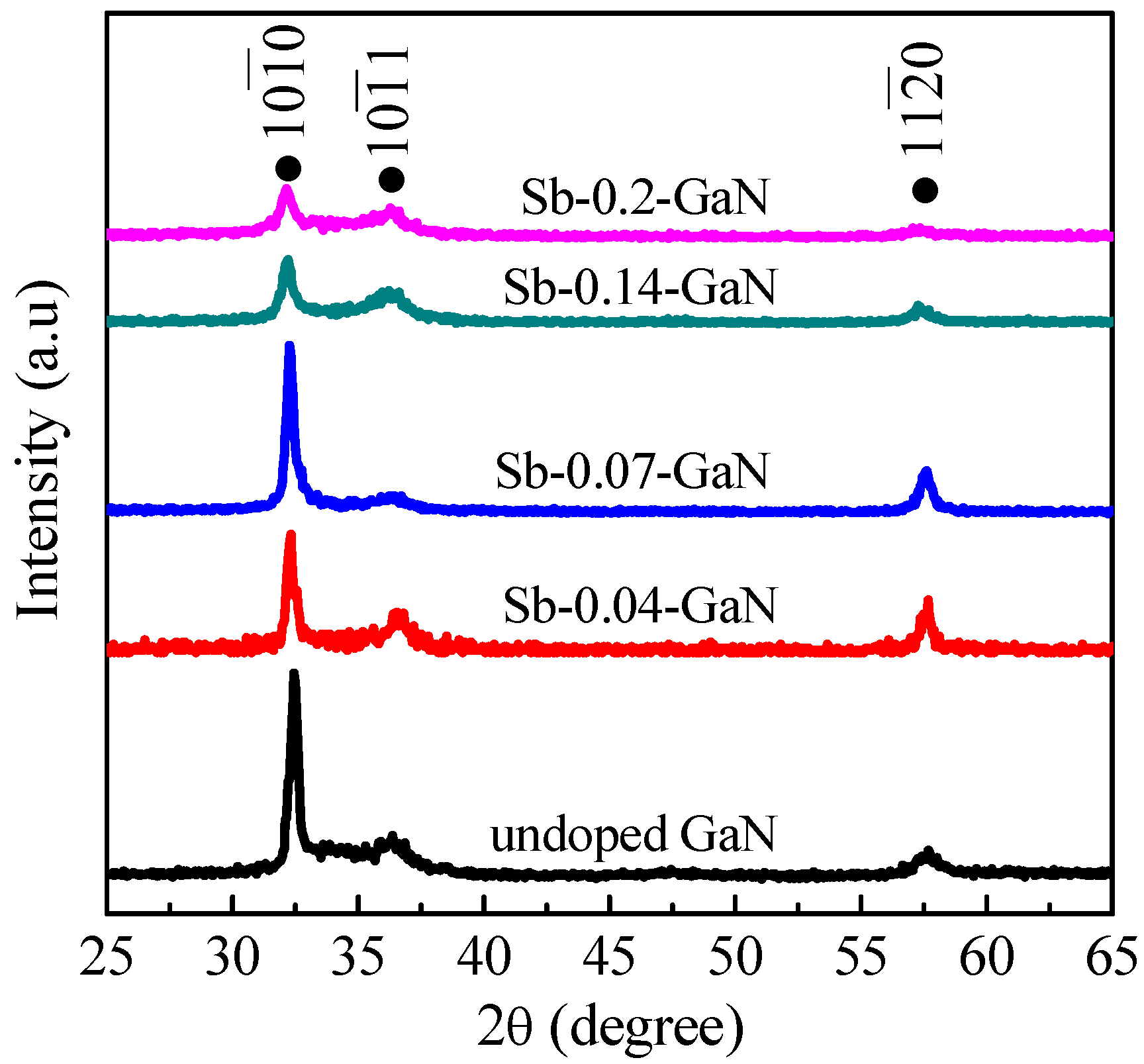
XRD patterns of the deposited Sb-
x-GaN films with different Sb precursor ratios of 0, 0.04, 0.07, 0.14, and 0.2 are presented in
Figure 3. Using the standard diffraction GaN data in PDF card No.76-0703, all sputtered Sb-
x-GaN films had the same structure of hexagonal wurtzite. The films were polycrystalline with the distinct diffractions from the (
),
, and (
) planes. The films had a preferential (
) plane of growth and no second phases. The diffraction intensity of (
) peak decreased due to the increase of Sb dopant concentration in the deposited films.
Table 2 lists all the investigated data from X-ray diffraction inspections. The (
) peak slightly shifted from 32.44° for Sb-0-GaN to 32.15° for Sb-0.2-GaN. It displayed that lattice constant of
a and
c, and the unit cell volume of Sb-
x-GaN films increased as there was an increment of Sb dopant content in the Sb-
x-GaN films. The lattice constant of
c was 5.09 Å for Sb-0-GaN and increased to 5.20, 5.21, 5.22, and 5.23 Å for Sb-
x-GaN with
x = 0.04, 0.07, 0.14, and 0.20, respectively. Besides,
a was 3.13 Å for Sb-0-GaN and increased to 3.19, 3.20, 3.21, and 3.22 Å for Sb-
x-GaN with
x = 0.04, 0.07, 0.14, and 0.20, respectively. Unit cell volumes increased with the increase in the Sb content of Sb-
x-GaN films, which were 43.18, 45.83, 46.26, 46.60, and 46.93 Å
3 at
x = 0, 0.04, 0.07, 0.14, and 0.2, respectively. From the 2θ value shown in
Table 2, the full width at half maxima (FWHM) values of the (
) peak possessed a slight increase from 0.31° for Sb-0-GaN and 0.32° for Sb-0.04-GaN to 0.35°, 0.42°, and 0.49° for Sb-
x-GaN at
x = 0.07, 0.14, and 0.2, respectively. Besides, the FWHM value of the (
) peak was a function of crystallite size. The crystallite sizes of films calculated with the Scherer equation were 29.7, 28.7, 26.3, 21.9, and 18.8 nm for the Sb-
x-GaN films at
x = 0, 0.04, 0.07, 0.14, and 0.20, respectively. There was a reduction in the crystallite sizes of Sb-
x-GaN from 29.7 to 18.8 nm with increasing the Sb content.
Figure 4 presents the surface morphology of Sb-
x-GaN films with individual cross-section SEM patterns in the insets. The surface SEM images displayed that the deposited Sb-GaN films had surface smoothness and microstructure with their grain size in a nanosized scale. From the vertical cross-section SEM patterns in the insets of
Figure 4, the thickness of Sb-
x-GaN films increased from (0.96 ± 0.05) µm for Sb-0-GaN to (1.20 ± 0.06) µm for Sb-0.2-GaN. These films adhered well on substrate without cracks and voids. As shown in
Table 3, the deposition rates of Sb-
x-GaN films at
x= 0, 0.04, 0.07, 0.14, and 0.2 were calculated to be (32.0 ± 1.6), (33.3 ± 1.6), (38.0 ± 1.9), (39.0 ± 2.0), and (40.0 ± 2.0) nm/min, respectively. There was a slight increment of the growth rate for the thicker film at higher Sb dopant content. It indicates that Sb accelerates the film growth.
AFM images of Sb-
x-GaN films after the 5 by 5 µm
2 dimensional scan are shown in
Figure 5. The root-mean-square (rms) roughness values of Sb-
x-GaN films were 0.76 ± 0.04, 0.88 ± 0.05, 1.48 ± 0.08, 1.26 ± 0.07, and 1.0 ± 0.05 nm as the antimony dopant content in Sb-
x-GaN films increased from
x = 0, 0.04, 0.07, 0.14, to 0.2, respectively, reaching a maximum for Sb-0.07-GaN. The surface roughness of the RF-sputtered GaN film was the range of 0.7–20 nm [
34], while it was 0.5–3 nm for GaN films grown by MOCVD [
35]. With surface roughness value of the RF-deposited Sb-
x-GaN films in the range from 0.76 ± 0.04 to 1.48 ± 0.08 nm, it indicated that the Sb-
x-GaN thin films were much smoother with the help of Sb incorporation.
Optical properties of grown Sb-
x-GaN films on quartz substrate were tested by UV–vis spectroscopy at 25 °C. From UV-vis data, the optical absorption coefficient and energy bandgap E
g of the Sb-
x-GaN films could be computed by using Tauc Equation (1) represented below.
where α is optical absorption coefficient of,
A is a constant,
hv is energy of the incident photon, and E
g is the energy band-gap of the Sb-
x-GaN thin films.
Figure 6 presents the plots of the (αhν)
2 − hν curves and extrapolation lines of the linear part of these plots. From these extrapolation lines, the energy bandgap of these films could be calculated and the E
g values of deposited Sb-
x-GaN film were 3.2, 3.04, 3.0, 2.81, and 2.72 eV for Sb-
x-GaN films at
x = 0, 0.04, 0.07, 0.14, and 0.2, respectively. From EDS composition analysis of Sb-
x-GaN films at
x = 0, 0.04, 0.07, 0.14, and 0.2 in the experiment, the [Sb]/([Sb]+[Ga]) molar ratios were 0, 1.6 ± 0.1, 2.8 ± 0.2, 9.7 ± 0.5, and 12.8 ± 0.7, respectively. The higher Sb content in Sb-
x-GaN target resulted the higher [Sb]/([Sb]+[Ga]) ratios in Sb-
x-GaN film, while their bandgap reduced from 3.2 to 2.72 eV, presenting the solid solution of Sb into GaN to cause the defect levels and to decrease in the energy bandgap. K. M. Yu reported that GaN
1−xSb
x alloys had the change of edge-absorption from 3.4 eV (GaN) to 1 eV for alloys containing more than 30 at.% Sb [
20]. Neugebauer et al. indicated that in p-type GaN the nitrogen vacancy (a donor) has the lowest formation energy, in n-type GaN the gallium vacancy (an acceptor) [
36]. Mattila et al. found clear confirmation for complicated formation between the positively charged donors and negatively charged cation vacancies [
37]. In the Sb-
x-GaN thin film, Sb not only behaved as an acceptor of Sb
3− in heavily doped GaN but also an isovalent dopant of Sb
3+.
Hall effect measurement system was applied to investigate the electrical characteristics of Sb-
x-GaN films at
x = 0, 0.04, 0.07, 0.14, and 0.2.
Figure 7 shows the variation of carrier concentration, mobility, and electrical conductivity of Sb-
x-GaN films (
x = 0, 0.04, 0.07, 0.14, and 0.2). The Hall effect measurement system was used to measure the carrier concentration and electrical mobility of Sb-x-GaN films. In this test, to prevent the measured current being affected from the
n-Si substrate, the first step to do before SbGaN deposition is to have a SiO
2 layer with 300 nm of thickness deposited on the n-Si substrate by DC magnetron sputtering, and then Sb-x-GaN film was deposited on SiO
2/n-Si substrate. Silver electrodes was deposited at the four corners to form a conductive electrode before measurement. The Hall effect measurement system uses the Lorentz force in the magnetic field to shift the direction of charge carriers. The difference in voltage caused by the accumulation of electrons or holes is to determine Sb-
x-GaN n-type or p-type. In this work, Sb-0-GaN and Sb-0.04-GaN films remained as a
n-type semiconductor. Sb-0-GaN film had average electron concentration (N
e) of (1.4 ± 0.1) × 10
17 cm
−3 and mobility of (3.0 ± 0.2) cm
2·V
−1·s
−1 (μ), while Sb-0.04-GaN film had the reduced N
e of (4.9 ± 0.3) × 10
15 cm
−3 and an increase of electron mobility (μ) of (17.0 ± 0.9) cm
2·V
−1·s
−1. It is important to note that Sb-0.07-GaN underwent the n-to-p transition stage. The Sb-0.07-GaN, Sb-0.14-GaN, and Sb-0.2-GaN films had an increase in positively charged carriers concentration from (5.2 ± 0.3) × 10
15, (2.9 ± 0.2) × 10
16, to (5.5 ± 0.3) × 10
17 cm
−3, respectively, while their electrical mobilities were 74 ± 4, 287 ± 15, and 165 ± 9 cm
2·V
−1·s
−1, respectively. It could be believed that Sb-0.07-GaN film experienced at the n-to-p transition stage and remained lower hole concentration of (5.2 ± 0.3) × 10
15 cm
−3. With a higher Sb content in target, Sb-0.14-GaN film contained higher hole concentration of (2.9 ± 0.2) × 10
16 cm
−3 and electrical mobility of (287 ± 15) cm
2.V
−1.s
−1. Sb-0.2-GaN film had the highest hole concentration of (5.5 ± 0.3) × 10
17 cm
−3, and hole mobility of (165 ± 9) cm
2.V
−1.s
−1. The highest hole concentration for Sb-0.2-GaN explained its lower mobility due to the increased hole concentration. After calculating the carrier concentration and electrical mobility, the electrical conductivity values are determined as (0.07 ± 0.01), (0.02 ± 0.01), (0.06 ± 0.01), (1.30 ± 0.07), and (14.5 ± 0.8) S·cm
-1 for Sb-
x-GaN films at
x = 0, 0.04, 0.07, 0.14, and 0.2, respectively. Electrical properties of Sb-
x-GaN films could be improved by the incorporation of Sb into GaN lattice. From EDS data in
Table 1, the [Sb]/([Sb]+[Ga]) molar ratios in the sputtered film were 0, 1.6 ± 0.1, 2.8 ± 0.2, 9.7 ± 0.5, and 12.8 ± 0.7, Sb contents added in SbGaN targets were 0, 4, 7, 14, and 20 at.%, respectively. There was an increase in the Sb dopant concentration in the films when the higher Sb content was in target. The increased Sb content in films led to the conversion of the
n-GaN into
p-GaN. Here is the explanation for the
n-to-
p conversion with the Sb substitution in GaN. The film composition is always the major factor in controlling its physical properties. The GaN film was anion deficient at the lower Sb content and cation deficient at the higher Sb content, as shown in
Table 1. It is the nitrogen vacancy to contribute the
n-type behavior and the gallium vacancy to the
p-type behavior.
The
p-type conduction behavior is enhanced at the higher Sb content in film with a lower cation/anion value less than 1.0 or more Ga vacancies, as shown in
Figure 7. With increasing the Sb content at the N site, the Sb-GaN crystal is supposed to have a huge expansion in unit cell. However, the expansion of unit cell by Sb substitution is limited due to the offset caused by the formation of Ga vacancy at the higher Sb content, as shown in
Table 2. With the big Sb anion on the N site and the formed Ga vacancies at a higher Sb content in the (Ga,Sb)(Sb,N) film, the lattice distortion becomes severe due to the complex lattice defects. Therefore, Sb-0.2-GaN film has shown the smaller crystallite size and worse crystallinity, as shown in
Figure 3. Basically, both of GaSb and GaN are
n-type semiconductors with band gaps of 0.726 and 3.4 eV and electron mobilities of 3000 and 1500 cm
2.V
−1·s
−1, respectively. Their mixture to form the alloy is expected to form lower bandgap, as shown in
Figure 6 for our data from 3.2 eV to 2.72 eV. However, in this work Sb in Sb-
x-GaN at a higher content of
x = 0.2 prefers to substitute the Ga cation site. The
n-to-
p conversion by incorporating Sb is special. Limited data were reported for the group V anion instead of cation doping on GaN [
18,
19,
20,
21,
22]. Our work can have its contribution on the HMA field for further development.
To further confirm Sb-
x-GaN films (at
x = 0.07, 0.14, and 0.2) acting as
p-type semiconductor, three hetero-junction diodes were prepared by Sb-0.07-GaN, Sb-0.14-GaN, and Sb-0.2-GaN films sputtered on
n-Si substrates, respectively. The electrical characteristics of
p-SbGaN/
n-Si hetero junction diodes were investigated by Semiconductor Device Analyzer (Agilent, B1500A) at the room temperature.
Figure 8 and
Figure 9 show the forward and reverse current density-voltage
J-V and log (
J)-
V characteristics, respectively, of
p-SbGaN/
n-Si diodes investigated from -20 to +20 V at 25 °C. The data from the
J-V curves display that the turn-on voltages are determined to be 1.5, 1.25, and 1.0 V for Sb-0.07-GaN, Sb-0.14-GaN, and Sb-0.2-GaN diode devices, respectively, while the breakdown voltages were above 20 V. At the 20 V forward bias, the Sb-0.2-GaN device had the highest current density of 0.253 A/cm
2, while they were 0.033 and 0.139 A/cm
2 for Sb-0.07-GaN and Sb-0.14-GaN devices. The parameters and the electrical properties of
p-SbGaN/
n-Si devices are listed in
Table 4. The leakage current density at −5 V was 2.70 × 10
−5, 5.13 × 10
−5, and 9.41 × 10
−5 A/cm
2 for
p-Sb-
x-GaN films at
x = 0.07, 0.14, and 0.20, respectively. It can be explained that the electrical properties of
p-Sb-0.07-GaN,
p-Sb-0.14-GaN, and
p-Sb-0.2-GaN films shown in
Figure 6 are related to the differences of leakage current density and forward current density of the diodes displayed in
Figure 8 and
Figure 9. The higher values of the leakage current density and the forward current density of
p-Sb-
x-GaN/
n-Si devices can result from the higher electrical conductivity for
p-Sb-
x-GaN films.
Using a standard thermionic-emission (TE) model as the mathematic statement, the electrical characteristics of the diode can be computed (for qV > 3kT). The equation is as shown below [
28,
29,
38,
39]:
where
q is the electron charge (1.60 × 10
−19 C),
I0 the saturation current,
V the supplied voltage,
n is the ideality factor,
Rs is the series resistance,
K is Boltzmann constant (1.38 × 10
−23 J·K
−1), and T is the experiment temperature in Kelvin. With the curve of
lnI versus V drawn by applying Equation (2), the saturation current
I0 can be retrieved by intersecting the interpolated straight line from the linear region of the semilog plot. The
I0 values were 1.38 × 10
−5, 7.60 × 10
−5 and 1.17 × 10
−4 A for
p-Sb-
x-GaN diodes at
x = 0.07, 0.14, and 0.2. With the help of the retrieved
I0 data, the barrier height can be found by using Equation (3) [
28,
38,
39].
where A is the area of the diode with the dimension of 1 × 1 mm
2,
A* the effective Richardson constant
K is Boltzmann constant (1.38 × 10
−23 J·K
−1), and T is the experiment temperature in Kelvin, and
he barrier height. In this formula, for
p-GaN diodes, the value of
A* in theory was computed to be 26.4 A.cm
−2·K
−2 with
m* = 0.22m
e, while the
A* was calculated to be 23 A·cm
−2·K
−2 with
m* = 0.19 m
e for
n-InGaN diodes [
25,
38]. The ideality factor n can be determined by the slope of the linear region in forward bias [
38,
40,
41]. It can be counted from the following equation:
From Equation (4) and
Figure 10 for the dV/d(lnI) versus current curves, the ideality factor
n can be computed to be 5.95, 6.12, and 6.54, and the barrier height
ϕB to be 0.49, 0.45, and 0.44 eV for Sb-
x-GaN diodes at
x = 0.07, 0.14, and 0.2, respectively.
Table 4 displays the electrical characteristics of Sb-
x-GaN diodes at
x = 0.07, 0.14, and 0.2. It is shown that the decrease of turn-on voltage is corelated with the lower barrier height.
Cheung’s equation is presented by the below equation and contains the series resistance
Rs and ideality factor
n [
38,
39,
40,
41,
42].
By using Equation (5), the
Rs series resistance and n ideality factor for the hetero-junction diodes were calculated and shown in
Table 4. The ideality factor n was 5.44, 5.59, and 5.94 and the series resistance
Rs was 8.34, 7.51, and 3.91 kΩ for Sb-
x-GaN diodes at
x = 0.07, 0.14, and 0.2, respectively. For Schottky diode, the ideality factor is often < 2. The ideality factors of our hetero junction diodes had higher values because of the high series resistances, which had been studied by the Cheungs’ method. The high
Rs series resistance also affects the current transport mechanism of the hetero junction diode. In addition to the reasons such as accelerated recombination of electrons and holes in depletion region, the occurrence of lattice distortion and the presence of crystalline and amorphous regions could also lead to the higher ideality factor in hetero junction diode [
23,
25,
29].

 ,
, 


