Abstract
Study of the strongly correlated states in van der Waals heterostructures is one of the central topics in modern condensed matter physics. Among these, the rhombohedral trilayer graphene (RTG) occupies a prominent place since it hosts a variety of interaction-driven phases, with the metallic ones yielding exotic superconducting orders upon doping. Motivated by these experimental findings, we show within the framework of the low-energy Dirac theory that the optical conductivity can distinguish different candidates for a paramagnetic metallic ground state in this system. In particular, this observable shows a single peak in the fully gapped valence-bond state. On the other hand, the bond-current state features two pronounced peaks in the optical conductivity as the probing frequency increases. Finally, the rotational symmetry breaking charge-density wave exhibits a minimal conductivity with the value independent of the amplitude of the order parameter, which corresponds precisely to the splitting of the two cubic nodal points at the two valleys into two triplets of the band touching points featuring linearly dispersing quasiparticles. These features represent the smoking gun signatures of different candidate order parameters for the paramagnetic metallic ground state, which should motivate further experimental studies of the RTG.
1. Introduction
Quasi-two-dimensional graphene-based van der Waals (vdW) heterostructures, such as bilayer and trilayer graphene, have recently emerged as a groundbreaking territory for the discovery of new electronic states of quantum matter driven by the electron interactions [1,2,3,4,5,6,7,8,9,10,11,12]. It is rather remarkable that by externally tuning the twist angle, doping, and/or the magnetic field, a new landscape of exotic insulating, metallic and superconducting states has been unearthed in these systems. Particularly prominent in this respect is the interplay between the metallic and the superconducting phases that gives rise to very rich phase diagrams (for a recent review, see Ref. [13]). However, their theoretical understanding is often hampered by the difficulty in distinguishing possible candidate ground states in these systems, as, for instance, when considering the emergence of superconductivity from a parent metallic state.
Rhombohedral trilayer graphene (RTG) has recently emerged as a rather prominent example in this respect, where superconducting instabilities are in proximity to metallic ground states in different doping regimes [11,12], with a few theoretical scenarios proposed to explain the rich phenomenology [14,15,16,17,18,19,20,21]. Most interestingly, very little is known about an exotic metal in the proximity of the experimentally identified SC1 order [12], except that it exhibits paramagnetic nature (see Extended Figure 7 in Ref. [12] and the discussion therein). In fact, a few candidates for such a state that may be driven by electron interactions have been identified, each of them breaking different microscopic symmetries: the valence-bond order (VBO), bond-current order (BCO), and smectic charge-density wave (sCDW) orders [16], respectively.
The optical conductivity is a well established tool in studying correlated electron materials, which is directly related to the excitation spectrum [22]. In particular, it has been studied in various vdW materials both theoretically [23,24,25,26,27,28] and experimentally [29,30]. In this work, we focus on the collisionless or high-frequency regime of the optical conductivity, pertaining to the frequencies , since in this regime, this observable shows a universal scaling that depends only on the form of the dispersion of the low-energy quasiparticles, the dimensionality of the system, and the scaling dimension of the electron–electron interactions [31]. Importantly, the scaling dimension of the optical conductivity in a d-dimensional system is equal to in units of momentum. Therefore, exactly in , at finite frequency and temperature, with other energy scales set to zero, , with as a universal dimensionless scaling function. In the limit , this function tends to a constant, yielding a universal amplitude for the collisionless optical conductivity.
Motivated by these developments, we show that the collisionless optical conductivity can distinguish different candidate paramagnetic metallic ground states in RTG. In particular, this observable shows a single peak in the fully gapped valence-bond state, as displayed in Figure 1a. On the other hand, the bond-current state features two pronounced peaks in the optical conductivity as the probing frequency increases, see Figure 1b. This behavior can be directly related to the Dirac nature of the valence-bond and the bond-current order parameters obeying, respectively, anticommutation and commutation relations with the single-particle noninteracting Hamiltonian given by Equation (1), and with the behavior of the density of states (DOS); see Figure 2a,b. Finally, the sCDW state is characterized by a minimal conductivity, which is independent of the amplitude of the sCDW order parameter [Figure 1c], and it corresponds precisely to the splitting of the two cubic nodal points at the two valleys into two triplets of linearly dispersing band touching points (Figure 3). This behavior is also consistent with the form of the DOS, particularly at low energies, displaying the linear scaling with the energy [Figure 2c]. As such, these characteristic features in the optical conductivity represent the smoking gun signatures of different candidate order parameters for the paramagnetic metallic ground state of the RTG. These, in turn, can serve as a starting point for the study of the superconductivity in this system and should motivate further its experimental study.
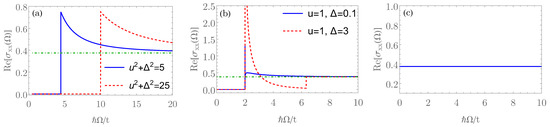
Figure 1.
Real part of the optical conductivity (in units of ) in the collisionless regime for: (a) the valence-bond order (VBO); (b) the bond-current order (BCO); (c) smectic charge-density wave (sCDW), respectively, given by Equations (6), (8), and (13), at the neutrality point and at . u and are given in units of the bandwidth scale t, see also the discussion after Equation (1). In panels (a,b), the green dashed line corresponds to the universal optical conductivity for the non-interacting spinless RTG in the collisionless regime, .
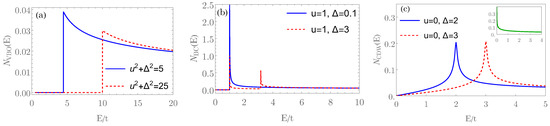
Figure 2.
The density of states (DOS) in the candidate paramagnetic states. (a) valence-bond order (VBO); (b) bond-current order (BCO); (c) smectic charge-density wave (sCDW). The DOS in the three phases is given in Equations (7), (11), and (S69) in the SI. The energy (E) is in units of the bandwidth (t), see also Figure 1. u and are given in units of t. The inset in (c) corresponds to the DOS for the noninteracting case, where the low-energy DOS scales as .
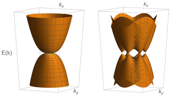
Figure 3.
The band structure for the noninteracting Hamiltonian given by Equation (1) (left panel), where the pairs of degenerate bands corresponding to the same valley are superimposed. In the smectic charge-density wave with the order parameter , , the two cubic band touching points split into six points, with the triplets featuring opposite vorticities (right panel). Notice that the smectic charge-density wave order parameter mixes the two valleys and, therefore, also breaks the original lattice translation symmetry, besides the rotational one. The rotational symmetry is, however, restored close to each of the new band touching points.
2. Model
We consider the effective low-energy model for the rhombohedral ( stacked) trilayer graphene obtained after integrating out high-energy degrees of freedom corresponding to the four gapped bands consisting of the states at the dimerized sites (one in the bottom (A), two in the middle (B), and one in the top (C) layer) [32,33,34]. Taking into account the layer (or equivalently sublattice) and valley degrees of freedom, the single-particle Hamiltonian for noninteracting electrons reads
where , nm is the lattice spacing within the single graphene layer, while eV and eV are the intralayer and the interlayer nearest-neighbor hoppings, respectively [33]. The corresponding bandwidth is given by the cutoff scale for the low-energy model in Equation (1), t∼∼ eV. The form factors , , respectively, transform under and representations of the point group of the RTG. Momentum is measured from the respective band-touching points (valleys). Electron (hole) doping corresponds to , and we set hereafter. The four-dimensional matrices are , where and are the sets of Pauli matrices that act on the valley and sublattice (layer) indices, respectively. Since we here consider only paramagnetic metallic states, we suppress the spin indices, see also Section S1 of the Supplemental Information (SI). Taking the possible patterns of symmetry breaking and the low-energy degrees of freedom, three candidates emerge in this respect [16]. First of all, the VBO, which fully gaps the system out and breaks the sublattice symmetry. Second, the BCO breaks, besides the sublattice symmetry, as well as the time-reversal. Finally, the sCDW breaks both the U(1) rotational symmetry about the axis, generated by the matrix , down to the discrete subgroup, and the lattice-translational symmetry, generated by the matrix . These three orders are represented by the following matrices ():
The corresponding irreducible representations of the group are and , for the VBO and BCO, respectively, while the sCDW transforms under the two-dimensional E representation. Notice that we now reduce the symmetry down to subgroup of the full point group of the noninteracting low-energy Hamiltonian in Equation (1) because we allow for the backscattering processes that mix the valleys, and in turn may yield the translational-symmetry breaking orders, such as the sCDW.
3. Optical Conductivity
To distinguish different candidate paramagnetic metallic ground states in RTG, we now compute the optical conductivity. To this end, we use the Kubo formula for the linear optical conductivity [35]
where the polarization tensor reads
Here, the velocity operator , is the Matsubara Green’s function, are the fermionic Matsubara frequencies, and the analytical continuation onto real frequencies is performed, , see also Section S2 of the SI for details.
4. Valence-Bond Order
We start by computing the optical conductivity for the simplest case, the VBO. The Hamiltonian is given by . Notice that since time-reversal symmetry (TRS) is preserved, the component of the polarization tensor vanishes. In addition, since rotational symmetry is conserved, , so we need to compute only one of the polarization tensor components. We then find, with the details shown in the SI, Section S3.A,
where is the quasiparticle dispersion, is the Fermi–Dirac distribution, and we defined . After performing the analytic continuation to real frequency, , we obtain the real part for the optical conductivity,
where is the universal optical conductivity for the noninteracting spinless RTG in the collisionless regime (in units ), and we defined . The technical details are presented in Section S3.A of the SI.
In Figure 1a, we can see a plot for the optical conductivity at zero temperature and at the neutrality point . Notice that the optical conductivity is zero until , where there is a maximum. This is expected, since is the gap between the conducting and valence bands. The asymptotic value is given by when .
To further elucidate the origin of the peaks in the optical conductivity in the VBO, we analyze the corresponding DOS
A remarkable feature of this expression is that the DOS develops a pole at the minimum of the conduction band , and hence it grows as compared to the gapless case . This effect manifests in an enhancement of the optical conductivity with the gap as compared to the universal value for the gapless case, as directly follows from Equation (6).
5. Bond-Current Order
We now follow the same procedure for the BCO case, where the Hamiltonian is given by . As for the VBO case, the rotation symmetry is preserved in the BCO, so . The real part of the optical conductivity then reads
Here, the functions and are defined by Equation (S45) in the SI, together with the dispersions
and the frequency-dependent coefficients
The optical conductivity is presented in Figure 1b, and it features two peaks, which represent hallmarks of this state. It is worth noticing that the weight of the conductivity peak at the lower frequency scales inversely with the amplitude of the order parameter . For the technical details, consult Section S3.B of the SI.
To further shed light on the presence of the two peaks in the optical conductivity, we analyze the corresponding DOS, with the form given in (Section S3.B of the SI)
where we used that in this case, the dispersion in each of the four bands is given by . This form of the band structure with two valence and two conduction bands, yielding the peaks in the DOS [Equation (11)], is therefore consistent with the form of optical conductivity in this phase, as shown in Figure 1b. We now analyze this observable in the remaining candidate phase for the paramagnetic metal, namely, the sCDW phase.
6. Charge Density Wave
The smectic charge-density wave yields a peculiar structure of the dispersion as it transforms under the two-dimensional E representation of the point group, with the vector realized in the valley space. As such, the sCDW mixes the valleys, with the bands given by
and the corresponding band structure shown in Figure 3. In fact, the sCDW splits two cubic band touching points, with the vorticity , living in the two valleys, into two triplets of the points with the vorticity , as explicitly shown in the SI, Section S3.C1. Furthermore, the form of the low-energy DOS, featuring the linear-E behavior, shown in Figure 2c, is consistent with the splitting of the nodal points in the sCDW phase. See also Section S3.C2 of the SI for the technical details.
We now compute the optical conductivity in the case when one of the components of this order parameter is nonzero, e.g., , and for the sake of the clarity, since the term ∼u acts as a gap, we also set . Furthermore, we take and , in the collisionless limit , with as the order-parameter amplitude, to obtain , with
with the technical details shown in Section S3.C3 of the SI. The identical results are obtained if instead we take to represent the sCDW order parameter, as expected from the corresponding commutation relations with the noninteracting Hamiltonian in Equation (1). In fact, the sCDW state can be thought of as a two-dimensional analogue of a correlation-driven nematic phase in a three-dimensional multi-Weyl semimetal [36].
This behavior of the optical conductivity is consistent with the splitting of the noninteracting band touching points with the vorticity of , into two triplets of the non-degenerate ones with the vorticity . We emphasize that the obtained form of the optical conductivity singles out the sCDW phase as compared with the previously discussed valence-bond and bond-current states. Finally, the obtained mean-field value of the conductivity is expected to decrease when fluctuations are taken into account due to the scattering between quantum-critical fermionic and bosonic excitations [37,38].
7. Conclusions and Outlook
In this paper, we showed that the optical conductivity can distinguish possible paramagnetic metallic ground states yielding a superconducting order in RTG, as shown in Figure 1. In particular, the valence-bond and bond-current states are distinguishable by the number of peaks in the optical conductivity, while this observable in the sCDW order features a minimum with a value matching the noniniteracting one at the mean-field level, due to the splitting of the cubically dispersing nodal points at each valley. We emphasize that we here analyze only the real part of the high-frequency optical conductivity due to its universal features. On the other hand, its imaginary part can be trivially obtained by integration over frequency via the Kramers–Kronig relation . However, its specific features are sensitive to (nonuniversal) microscopic details, such as the bandwidth, and hence, it does not provide a direct probe of the possible interaction-driven ground states in RTG.
The approach employed for the identification of the possible interaction-driven metallic ground states is quite general and can be applied to other vdW systems to distinguish possible correlated insulating and metallic states, as in the case of twisted bilayer graphene [27]. The same applies to the case of Bernal bilayer graphene (without twist) and other vdW materials, such as MoS and WSe, where an analogous analysis can also be used to distinguish possible interaction-driven metallic ground states.
We here emphasize that our conclusions are based on the mean-field picture where the role of the fluctuations on the conductivity has been neglected. To account for the further corrections in the quantum-critical regime, we need to address the full quantum-critical theory describing the quantum-critical transition, as, for instance, in case of monolayer graphene [37], and we plan to investigate this problem in the future. Another open avenue emerging from this work concerns the features of the interaction-driven phases in vdW materials in the nonlinear transport [38]. Finally, our findings should stimulate future theoretical and experimental work on the out-of-plane optical response of the vdW materials [39], and particularly, the role of the electron–electron interactions in this respect.
Supplementary Materials
The following supporting information can be downloaded at: https://www.mdpi.com/article/10.3390/nano12213727/s1, In the Supplementary Information we provide additional technical details to support the results and conclusions presented in the main text of the article. Supplementary Information contains the following sections: S1. Low-energy model for trilayer graphene; S2. Optical conductivity in the Kubo linear-response formalism; S3. Paramagnetic metal; S3.A. Valence bond order; S3.B. Bond current; S3.C. Smectic charge-density wave; S3.C1. Splitting of the band touching points; S3.C2. Density of states; S3.C3. Optical conductivity.
Author Contributions
Conceptualization, V.J., E.M., R.S.-G.; formal analysis, V.J., E.M., R.S.-G.; writing—review and editing, V.J., E.M., R.S.-G. All authors have read and agreed to the published version of the manuscript.
Funding
This research was funded by Fondecyt grants number 1190361 and 1200399, by ANID PIA Anillo ACT/192023 and the Swedish Research Council Grant No. VR 2019-04735 (V.J.). Nordita is partially supported by Nordforsk. The APC was funded by Stockholm University.
Institutional Review Board Statement
Not applicable.
Informed Consent Statement
Not applicable.
Data Availability Statement
Not applicable.
Acknowledgments
The authors are grateful to Bitan Roy for useful discussions.
Conflicts of Interest
The authors declare no conflict of interest.
References
- Cao, Y.; Fatemi, V.; Demir, A.; Fang, S.; Tomarken, S.L.; Luo, J.Y.; Sanchez-Yamagishi, J.D.; Watanabe, K.; Taniguchi, T.; Kaxiras, E.; et al. Correlated insulator behaviour at half-lling in magic-angle graphene superlattices. Nature 2018, 556, 80. [Google Scholar] [CrossRef] [PubMed]
- Cao, Y.; Fatemi, V.; Fang, S.; Watanabe, K.; Taniguchi, T.; Kaxiras, E.; Jarillo-Herrero, P. Unconventional superconductivity in magic-angle graphene superlattices. Nature 2018, 556, 43. [Google Scholar] [CrossRef] [PubMed]
- Lu, X.; Stepanov, P.; Yang, W.; Xie, M.; Aamir, M.A.; Das, I.; Urgell, C.; Watanabe, K.; Taniguchi, T.; Zhang, G.; et al. Superconductors, orbital magnets and correlated states in magic-angle bilayer graphene. Nature 2019, 574, 653. [Google Scholar] [CrossRef] [PubMed]
- Jiang, Y.; Lai, X.; Watanabe, K.; Taniguchi, T.; Haule, K.; Mao, J.; Andrei, E.Y. Charge order and broken rotational symmetry in magic-angle twisted bilayer graphene. Nature 2019, 573, 91. [Google Scholar] [CrossRef]
- Yankowitz, M.; Chen, S.; Polshyn, H.; Zhang, Y.; Watanabe, K.; Taniguchi, T.; Graf, D.; Young, A.F.; Dean, C.R. Tuning superconductivity in twisted bilayer graphene. Science 2019, 363, 1059. [Google Scholar] [CrossRef]
- Chen, G.; Sharpe, A.L.; Gallagher, P.; Rosen, I.T.; Fox, E.J.; Jiang, L.; Lyu, B.; Li, H.; Watanabe, K.; Taniguchi, T.; et al. Signatures of tunable superconductivity in a trilayer graphene moiré superlattice. Nature 2019, 572, 215. [Google Scholar] [CrossRef]
- Liu, X.; Hao, Z.; Khalaf, E.; Lee, J.Y.; Ronen, Y.; Yoo, H.; Haei Najafabadi, D.; Watanabe, K.; Taniguchi, T.; Vishwanath, A.; et al. Tunable spin-polarized correlated states in twisted double bilayer graphene. Nature 2020, 583, 221. [Google Scholar] [CrossRef]
- Serlin, M.; Tschirhart, C.; Polshyn, H.; Zhang, Y.; Zhu, J.; Watanabe, K.; Taniguchi, T.; Balents, L.; Young, A. Intrinsic quantized anomalous hall effect in a moiré heterostructure. Science 2020, 367, 900. [Google Scholar] [CrossRef]
- Park, J.M.; Cao, Y.; Watanabe, K.; Taniguchi, T.; Jarillo-Herrero, P. Tunable strongly coupled superconductivity in magic-angle twisted trilayer graphene. Nature 2021, 590, 249. [Google Scholar] [CrossRef]
- Rubio-Verdú, C.; Turkel, S.; Song, Y.; Klebl, L.; Samajdar, R.; Scheurer, M.S.; Venderbos, J.W.; Watanabe, K.; Taniguchi, T.; Ochoa, H.; et al. Moire nematic phase in twisted double bilayer graphene. Nat. Phys. 2022, 18, 196. [Google Scholar] [CrossRef]
- Zhou, H.; Xie, T.; Ghazaryan, A.; Holder, T.; Ehrets, J.R.; Spanton, E.M.; Taniguchi, T.; Watanabe, K.; Berg, E.; Serbyn, M.; et al. Half- and quarter-metals in rhombohedral trilayer graphene. Nature 2021, 598, 429. [Google Scholar] [CrossRef] [PubMed]
- Zhou, H.; Xie, T.; Taniguchi, T.; Watanabe, K.; Young, A.F. Superconductivity in rhombohedral trilayer graphene. Nature 2021, 598, 434. [Google Scholar] [CrossRef] [PubMed]
- Törmä, P.; Peotta, S.; Bernevig, B.A. Superconductivity, superuidity and quantum geometry in twisted multilayer systems. Nat. Rev. Phys. 2022, 4, 528. [Google Scholar] [CrossRef]
- Chou, Y.-Z.; Wu, F.; Sau, J.D.; Das Sarma, S. Acoustic-phonon-mediated superconductivity in rhombohedral trilayer graphene. Phys. Rev. Lett. 2021, 127, 187001. [Google Scholar] [CrossRef]
- Ghazaryan, A.; Holder, T.; Serbyn, M.; Berg, E. Unconventional superconductivity in systems with annular fermi surfaces: Application to rhombohedral trilayer graphene. Phys. Rev. Lett. 2021, 127, 247001. [Google Scholar] [CrossRef]
- Szabó, A.L.; Roy, B. Metals, fractional metals, and superconductivity in rhombohedral trilayer graphene. Phys. Rev. B 2022, 105, L081407. [Google Scholar] [CrossRef]
- Cea, T.; Pantaleón, P.A.; Phong, V.T.; Guinea, F. Superconductivity from repulsive interactions in rhombohedral trilayer graphene: A kohn-luttinger-like mechanism. Phys. Rev. B 2022, 105, 075432. [Google Scholar] [CrossRef]
- Dai, H.; Hou, J.; Zhang, X.; Liang, Y.; Ma, T. Mott insulating state and d + id superconductivity in an abc graphene trilayer. Phys. Rev. B 2021, 104, 035104. [Google Scholar] [CrossRef]
- You, Y.-Z.; Vishwanath, A. Kohn-luttinger superconductivity and intervalley coherence in rhombohedral trilayer graphene. Phys. Rev. B 2022, 105, 134524. [Google Scholar] [CrossRef]
- Chatterjee, S.; Wang, T.; Berg, E.; Zaletel, M.P. Intervalley coherent order and isospin uctuation mediated superconductivity in rhombohedral trilayer graphene. arXiv 2021, arXiv:2109.00002. [Google Scholar]
- Dong, Z.; Levitov, L. Superconductivity in the vicinity of an isospin-polarized state in a cubic dirac band. arXiv 2021, arXiv:2109.01133. [Google Scholar]
- Basov, D.N.; Averitt, R.D.; van der Marel, D.; Dressel, M.; Haule, K. Electrodynamics of correlated electron materials. Rev. Mod. Phys. 2011, 83, 471. [Google Scholar] [CrossRef]
- Tabert, C.J.; Nicol, E.J. Optical conductivity of twisted bilayer graphene. Phys. Rev. B 2013, 87, 121402. [Google Scholar] [CrossRef]
- Moon, P.; Koshino, M. Optical absorption in twisted bilayer graphene. Phys. Rev. B 2013, 87, 205404. [Google Scholar] [CrossRef]
- Stauber, T.; San-Jose, P.; Brey, L. Optical conductivity, drude weight and plasmons in twisted graphene bilayers. New J. Phys. 2013, 15, 113050. [Google Scholar] [CrossRef]
- Jang, J.; Ahn, S.; Min, H. Optical conductivity of black phosphorus with a tunable electronic structure. 2D Mater. 2019, 6, 025029. [Google Scholar] [CrossRef]
- Calderón, M.J.; Bascones, E. Correlated states in magic angle twisted bilayer graphene under the optical conductivity scrutiny. npj Quantum Mater. 2020, 5, 57. [Google Scholar] [CrossRef]
- Tan, C.J.; Yan, C.-X.; Zhao, Y.-H.; Guo, H.; Chang, H.-R. Anisotropic longitudinal optical conductivities of tilted Dirac bands in 1T’-MoS2. Phys. Rev. B 2021, 103, 125425. [Google Scholar] [CrossRef]
- Song, B.; Gu, H.; Fang, M.; Ho, Y.T.; Chen, X.; Jiang, H.; Liu, S. Complex optical conductivity of twodimensional mos2: A striking layer dependency. J. Phys. Chem. Lett. 2019, 10, 6246. [Google Scholar] [CrossRef]
- Zhang, G.; Huang, S.; Wang, F.; Xing, Q.; Song, C.; Wang, C.; Lei, Y.; Huang, M.; Yan, H. The optical conductivity of few-layer black phosphorus by infrared spectroscopy. Nat. Commun. 2020, 11, 1847. [Google Scholar] [CrossRef]
- Sachdev, S. Quantum Phase Transitions, 2nd ed.; Cambridge University Press: Cambridge, UK, 2011. [Google Scholar]
- Koshino, M.; McCann, E. Trigonal warping and Berry’s phase Nπ in ABC-stacked multilayer graphene. Phys. Rev. B 2009, 80, 165409. [Google Scholar] [CrossRef]
- Zhang, F.; Sahu, B.; Min, H.; MacDonald, A.H. Band structure of abc-stacked graphene trilayers. Phys. Rev. B 2010, 82, 035409. [Google Scholar] [CrossRef]
- Cvetkovic, V.; Vafek, O. Topology and symmetry breaking in abc trilayer graphene. arXiv 2012, arXiv:1210.4923. [Google Scholar]
- Mahan, G.D. Many-Particle Physics; Springer Science & Business Media: Berlin/Heidelberg, Germany, 2013. [Google Scholar]
- Roy, B.; Goswami, P.; Juričić, V. Interacting weyl fermions: Phases, phase transitions, and global phase diagram. Phys. Rev. B 2017, 95, 201102. [Google Scholar] [CrossRef]
- Roy, B.; Juričić, V. Collisionless transport close to a fermionic quantum critical point in dirac materials. Phys. Rev. Lett. 2018, 121, 137601. [Google Scholar] [CrossRef]
- Rostami, H.; Juričić, V. Probing quantum criticality using nonlinear Hall effect in a metallic Dirac system. Phys. Rev. Res. 2020, 2, 013069. [Google Scholar] [CrossRef]
- Xu, Z.; Ferraro, D.; Zaltron, A.; Galvanetto, N.; Martucci, A.; Sun, L.; Yang, P.; Zhang, Y.; Wang, Y.; Liu, Z.; et al. Optical detection of the susceptibility tensor in two-dimensional crystals. Commun. Phys. 2021, 4, 215. [Google Scholar] [CrossRef]


Publisher’s Note: MDPI stays neutral with regard to jurisdictional claims in published maps and institutional affiliations. |
© 2022 by the authors. Licensee MDPI, Basel, Switzerland. This article is an open access article distributed under the terms and conditions of the Creative Commons Attribution (CC BY) license (https://creativecommons.org/licenses/by/4.0/).