Abstract
With the widespread diffusion of personal Internet of Things (IoT) devices, Electromagnetic Side-Channel Attacks (EM-SCAs), which exploit electromagnetic emissions to uncover critical data such as cryptographic keys, are becoming extremely common. Existing shielding approaches typically rely on bulky or opaque materials, which limit integration in modern IoT environments; this motivates the need for a transparent, lightweight, and easily integrable solution. Thus, to address this threat, we propose the use of electromagnetic metasurfaces with shielding capabilities, fabricated with an optically transparent conductive film. This film can be easily integrated into glass substrates, offering a novel and discrete shielding solution to traditional methods, which are typically based on opaque dielectric media. The paper presents two proof-of-concept case studies for shielding against EM-SCAs. The first one investigates the design and fabrication of a passive metasurface aimed at shielding emissions from chip processors in IoT devices. The metasurface is conceived to attenuate a specific frequency range, characteristic of the considered IoT processor, with a target attenuation of 30 dB. At the same time, the metasurface ensures that signals from 4G and 5G services are not affected, thus preserving normal wireless communication functioning. Conversely, the second case study introduces an active metasurface for dynamic shielding/transmission behavior, which can be modulated through diodes according to user requirements. This active metasurface is designed to block undesired electromagnetic emissions within the 150–465 MHz frequency range, which is a common band for screen gleaning security threats. The experimental results demonstrate an attenuation of approximately 10 dB across the frequency band when the shielding mode is activated, indicating a substantial reduction in signal transmission. Both the case studies highlight the potential of transparent metasurfaces for secure and dynamic electromagnetic shielding, suggesting their discrete integration in building windows or other environmental structural elements.
1. Introduction
In today’s digital world, most daily activities rely on personal devices that continuously and wirelessly exchange sensitive information over the Internet. As a result, data security and privacy are constantly at risk, necessitating targeted and strategic protection measures that effectively balance threats, costs, and benefits. In particular, the Internet of Things (IoT) concept is increasingly prevalent in homes, offices, and urban environments, enhancing quality of life at the expenses of massively collecting and transmitting sensitive user data, including health information [1], location tracking, and behavioral patterns. Furthermore, many IoT devices are integrated into critical infrastructures (as hospitals and industrial plants), and their compromise can lead to severe consequences [2], such as accidents, service disruptions, identity thefts, and privacy violations.
Among the most significant security threats, network-based attacks, such as Man-in-the-Middle (MitM) and Denial of Service (DoS), data breaches, firmware hijacking, and application-level threats such as malware and ransomware are extremely diffused. The MitM is a cyberattack where an attacker secretly intercepts and possibly alters communication between two parties without their knowledge. It is especially used to steal sensitive information like login credentials or financial data. Instead, the DoS is an attack that aims to make a system, service, or network unavailable by overwhelming it with excessive traffic or exploiting vulnerabilities, causing disruption for legitimate users. Additionally, sensors and wireless communications are susceptible to tampering and jamming, raising substantial privacy concerns.
Besides these, another particularly insidious class of cyber threats is side-channel attacks, which exploit physical characteristics of a system rather than targeting its software logical execution flow [3,4]. These attacks acquire external information, such as power consumption, electromagnetic emissions, execution time, and acoustic noise, to infer sensitive data [5,6]. Side-channel attacks can be categorized as active or passive, and invasive or non-invasive. Active attacks interfere with device functionality, such as fault injection attacks that induce errors in cryptographic processes. Passive attacks, in contrast, collect side-channel data without disrupting the device. Invasive attacks physically manipulate the device to access internal components, while non-invasive attacks analyze external emissions, such as execution time and power consumption.
This study focuses on mitigating passive and non-invasive attacks, particularly Electromagnetic Side-Channel Attacks (EM-SCAs). Variations in electrical signals within a device generate electromagnetic emissions that correlate with basically every computational process, potentially exposing critical information such as cryptographic keys [7]. Even when cryptographic algorithms are theoretically secure, their physical implementation may introduce vulnerabilities exploitable through EM radiation analysis [8,9].
To counteract these risks, both software- and hardware-based countermeasures can be implemented [10]. Software techniques, such as masking cryptographic operations, obscure side-channel signals, making it more difficult for attackers to extract meaningful information [11,12,13,14]. On the other hand, hardware approaches focus on controlling electromagnetic undesired emissions coming from the physical operation of devices, primarily through shielding. Traditional shielding materials (e.g., aluminum, copper, and steel) create physical barriers that prevent unauthorized EM signal leakage, but they have limitations in terms of weight, flexibility, and frequency range coverage.
Therefore, the scientific community leads its attention to an innovative alternative involving artificially designed metamaterials, which present unique electromagnetic properties not found in conventional materials [15,16]. They consist in 3D or 2D matrices of subwavelength unit-cells, thus interpreted as a homogenous material by the impinging radiation. The unit-cell characteristics confer the overall metamaterial response in terms of reflection, transmission and absorption [17]. Metamaterials offer unprecedented control over the propagation and interaction of electromagnetic waves, a concept first recognized in the late 1960s [18,19], and further developed over the following decades [20,21]. This ability allows them to overcome the intrinsic limitations of conventional shielding approaches, with a versatility demonstrated across a wide range of applications. Examples include biomedical technologies, where tailored designs enhance compatibility and minimize unwanted exposure [22,23]; high-performance, low-visibility antennas for advanced communication systems [24,25]; and stealth solutions in the military and automotive sectors aimed at reducing radar cross-section [26,27]. Moreover, multilayer metamaterial structures with engineered frequency-selective properties enable novel filtering functionalities [28,29], while their unique resonant responses have been exploited to achieve efficient wireless power transfer [30,31], and energy harvesting from ambient electromagnetic fields [32,33]. When deployed in their 2D version, i.e., metasurfaces, their lightweight and flexible nature facilitates seamless integration into existing devices and infrastructures without adding significant bulk. Consequently, metamaterials and metasurfaces offer a promising solution for enhancing cybersecurity, improving the protection of communications, data, and critical systems in an increasingly interconnected digital landscape.
In particular, several studies have recently investigated the use of metasurfaces for mitigating EM-SCAs, mainly focusing on one of two aspects: either the design of intelligent electromagnetic materials, often frequency-selective filters used to fully or partially shield rooms or buildings [34,35], or the use of metamaterials to introduce signal alterations that are leveraged by recognition algorithms as EM fingerprints, leading to notable advancements and improvements in cryptographic operations and techniques [36]. The first aspect is also exemplified by attempts to shield indoor spaces from 5G signals [37] or integrate frequency selective surface (FSS) into building facades and wall partitions to selectively isolate specific frequency bands [38] or to stop the Wi-Fi service [39]. These studies enhance cybersecurity but as part of a broader goal: developing smart buildings that also reduce occupants’ exposure to electromagnetic radiation and, when combined with energy harvesting circuits, enable the conversion of EM energy into electrical power.
However, limited attention has been devoted by the aforementioned studies to the physical realization of these metasurfaces and to the corresponding practical implications. Typically, metasurfaces are fabricated using printed circuit board (PCB) techniques, where metallic patterns are layered onto dielectric substrates such as FR4, or on flexible supports like polyimide. These conventional materials, however, are optically opaque, which limits their applicability in discrete scenarios requiring transparency, such as integration onto sensitive architectural elements like building windows. Several studies on electromagnetic metasurfaces have highlighted optical transparency as a desirable feature, often achieved through alternative materials such as metal meshes or silver nanowires [40,41,42]. However, metal meshes present significant challenges in terms of manufacturing and integration, particularly for architectural applications like windows, where uniformity and aesthetic quality are critical.
To fill this gap, we herein propose the use of optically transparent conductive films for the realization of metasurfaces that can be integrated into glass substrates. As a matter of fact, glass interfaces, as windows, are the weakest points from an electromagnetic security point of view. Figure 1 illustrates the propagation of electromagnetic waves emitted by a smartphone inside a room. The waves extend up to the glass interface, where the optically transparent shielding layer effectively blocks their transmission, thus preventing leakage to the external environment while preserving full optical visibility. Specifically, we present two proof-of-concept case studies: the first involves a passive metasurface designed to shield emissions from the processors of IoT devices; the second demonstrates an active shielding solution for suppressing screen gleaning emissions, illustrating how the switching capabilities of the material can be exploited not only for shielding purposes but also for controlled information modulation.
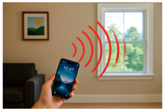
Figure 1.
Application context: spurious electromagnetic waves (constituting the side channel) generated by a smartphone are stopped by the transparent shielding on the glass preventing transmission beyond it (picture generated through AI tool).
The following sections provide a comprehensive overview of the development and performance evaluation of the two conceived metamaterials. Section 2 focuses on the passive screen as a device attack countermeasure, starting with a detailed description of the scenario motivating the study, followed by the design and fabrication process of the passive panel. The chapter concludes with an assessment of the panel’s performance through experimental measurements. Conversely, Section 3 presents the design and implementation of an active protection mechanism based on a reconfigurable FSS along with the description of the application scenario. It elaborates on the design considerations necessary for integrating active elements into the screening structure and provides a thorough evaluation of the active panel’s performance, emphasizing its capability to dynamically switch between operational states. Finally, Section 4 summarizes the key findings of this work, discusses their implications, and outlines potential directions for future research in the field of adaptive electromagnetic shielding.
2. Passive Screen
EM radiation can be generated by various components of an IoT device, and, among them, the processor proves to be the most significant from a forensic point of view. Several investigations have proved that the EM emission patterns of the CPU can be correlated with the software activities of the device [43]. The implementation of opportune electromagnetic shielding, particularly for IoT devices, requires a balance between effectiveness, cost, miniaturization, and environmental adaptability. Overcoming these challenges is essential to develop secure and reliable devices that are capable of operating without unwanted interference and protecting sensitive information from potential threats.
2.1. Application Scenario
An attacker with a high-gain, highly directional antenna and correct polarization matching can conduct an EM-SCA on a device, even from a tens-of-meters order distance, extracting sensitive information. Environmental vulnerabilities, such as electromagnetically poorly shielded glass walls or windows, can facilitate these attacks by allowing radio and microwave frequency leakage.
Traditional Faraday cages may not be an ideal shielding solution, as they indiscriminately block all frequencies, including those essential for device functionality. For example, shielding a banking facility with a Faraday cage would prevent attackers from intercepting signals but would also disrupt necessary communication technologies such as cellular networks and Wi-Fi, Figure 2.
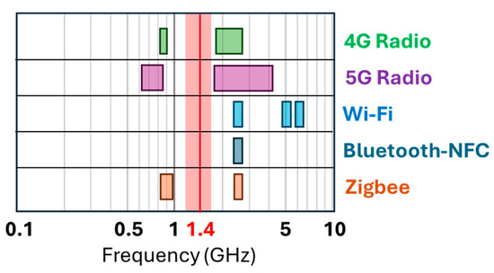
Figure 2.
Common wireless technologies frequency bands together with the frequency carrier and band emitted by the CPU in [43].
A more effective alternative can be the adoption of FSS to shield vulnerable structural elements like windows and exterior walls. These electromagnetically engineered materials can be designed to block only the frequencies that pose security risks while allowing necessary communication signals to pass, ensuring both security and device functionality, Figure 2.
As a representative test-case to characterize the typical electromagnetic behaviour of the entire class of high-end IoT devices which are capable of performing complex operations such as the cryptographic ones, the extremely diffused ARM Cortex-A53 1.4 GHz, quad-core processor (ARM Holdings, Cambridge, UK) is used [43]. A Raspberry Pi 3 B+ can be employed to this aim, which is equipped with such processor. It has been shown that the power spectral density of its electromagnetic emissions presents a maximum around its clock frequency with a bandwidth of about 20 MHz. To effectively measure the emitted electromagnetic waves, an H-loop antenna can be strategically placed 1 cm above the processor. This information has been used to define the stopband requisites of the FSS material (centre frequency, bandwidth, target attenuation) required for the shielding, summarized in Table 1. To avoid perturbing signals from 4G and 5G services, the filter stop band is fixed to 200 MHz.

Table 1.
Stop band filtering properties for the FSS design to protect the ARM CORTEX-A53 processor.
An attenuation level peak of 30 dB represents a substantial reduction in the signal at 1.4 GHz. For an attacker, compensating for such a significant attenuation through an increase in the receiving antenna’s gain is often not technically feasible or economically viable in most practical scenarios. As a result, a malicious eavesdropper trying to intercept the signal would not be able to rely solely on improving the antenna’s gain and would be forced to physically approach the signal source, exposing itself to the risk of detection. This consequence makes the use of FSS an effective strategy to mitigate unauthorized signal interception.
2.2. Design and Realization of the FSS Passive Panel
FSS configurations with a ring as unit cell are often designed to function as a high-pass filter, but they can also be conceived to act as a notch filter when operating around their self-resonance frequency [21]. In this case the rings can be specifically designed to block or reflect signals at a fixed frequency band, while frequencies outside this band pass through the screen.
The optimized unit cell, shown in Figure 3a,b, is composed of a single transparent Indium Tin Oxide (ITO) based conductive film ring (2.5 Ω/sq), whose inner and outer radii, R1 and R2, are equal to 28 mm and 32 mm, respectively. The design optimization was performed by parameterizing the inner and outer radii of the ITO loop. The loop is then sandwiched between two glass layers with a thickness W of 2 mm, as illustrated in Figure 3c. As a matter of fact, alternative unit-cell designs—such as the split-ring—could achieve a similar shielding response with a more compact size. However, since 1.4 GHz does not impose stringent constraints on unit-cell dimensions, we opted to keep the laser-cut fabrication process as simple as possible, thereby minimizing both cost and potential manufacturing inaccuracies. A passive square panel consisting of 5 × 5 cells has been constructed by manually cut and repeating the unit cell five times along both the x- and y-axes, with a periodicity P of 74 mm, as shown in Figure 3d. The final structure, with lateral dimensions of 60 cm × 60 cm, was assembled by embedding the array between two glass layers. Prior to sealing, a thin layer of spray adhesive was applied to ensure proper bonding. The fabricated prototype of the optically transparent passive screen, with the FSS integrated between two glass sheets, is shown in Figure 4. Notably, the overall optical transmittance of the prototype was conservatively estimated from the adopted materials properties. Considering two 2 mm glass layers (exhibiting 90% transmittance each), a 100 nm ITO film (presenting an 85% transmittance), and reflection losses at four interfaces, the calculated total transmittance was 59%, which is within the range generally regarded as transparent for architectural integration.
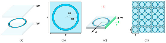
Figure 3.
Transparent passive panel description: (a) exploded view of the unit cell, (b) shape, size and periodicity of the unit cell, (c) reference system for the repetition of the cells, and (d) the FSS panel prototype composed by a 5 × 5 cell array. Parameters values are listed in Table 2.
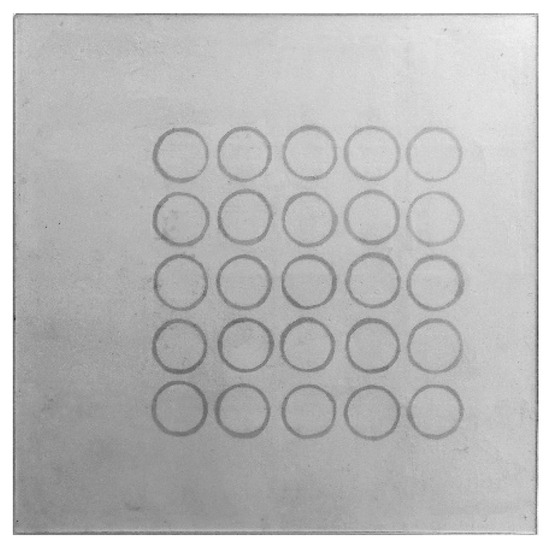
Figure 4.
Realization of the optically transparent passive screen with the FSS layer integrated between two glass sheets. The 60 cm × 60 cm panel is photographed on a white background to enhance the visibility of the FSS layer.
Table 2.
Geometrical dimensions of the stop band FSS panel.
Table 2.
Geometrical dimensions of the stop band FSS panel.
| Geometrical Parameters | (mm) |
|---|---|
| Internal radius—R1 | 28 |
| External radius—R2 | 32 |
| Periodicity—P | 74 |
| Glass substrate thickness—W | 2 |
2.3. Performance Measurement
The next step aimed at validating numerically and experimentally the effectiveness of the FSS designed to shield electromagnetic signals at 1.4 GHz. The numerical simulations were carried out with Feko 2025 software (Altair, Troy, MI, USA) implementing a Method of Moments solver and representing the array as infinite through periodic boundary conditions.
Conversely, the measurements were conducted in an anechoic chamber, a controlled environment that minimizes electromagnetic reflections and external noise, ensuring accurate testing conditions, Figure 5a. Two broadband dipole antennas were used (PCD-3100 and PCD-8250, Ref. [44]), placed 80 cm apart and opposite each other in polarization matching, so as to maximize the received signal under free-space conditions. Additionally, plastic supports were employed to hold the FSS panel in position without altering the electromagnetic behavior and ensuring that the surface was exposed to a normal incidence, as specified during the design phase.
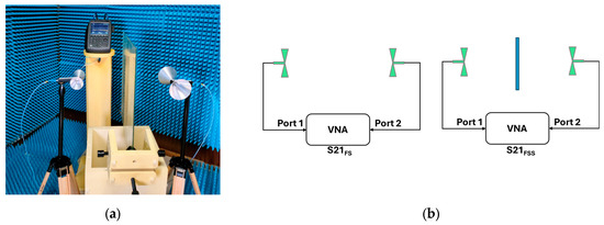
Figure 5.
Set-up for performance measurement: (a) anechoic chamber environment, showing the panel under test placed between the two antennas, in turn connected to the Vector Network Analyzer, and (b) flowchart outlining the two-step measurement process of the transmission coefficient.
The panel performance is evaluated through the transmission coefficient , defined as the logarithmic ratio between the electromagnetic coupling measured between the two antennas in the presence of the frequency selective surface and that corresponding to the free-space link, as illustrated in Figure 5b:
where denotes the transmission coefficient measured when the frequency selective surface is present, and represents the transmission coefficient of the free-space reference configuration.
τ = 20∙log10 (S21, FSS/S21, FS)
The numerically obtained and the measured transmission coefficients are compared in Figure 6, showing a good agreement between the two datasets. Specifically, the panel reveals a notch frequency band of 200 MHz around 1.4 GHz, thus satisfactorily matching the required performance described in Table 1. Moreover, we numerically investigated the angular robustness of the solution for both TE and TM polarizations. Although the structure is centro-symmetric and therefore polarization-independent at normal incidence, this property no longer holds as the incidence angle increases. Figure 7 shows the numerical simulations for incidence angles up to 45°. It is evident that while both polarizations exhibit consistent behavior at the operating frequency of 1.4 GHz, the TE polarization becomes less stable in the higher frequency range, where a stopband appears around 2.6 GHz. Although this issue is not critical for the proposed application, it is nevertheless essential to consider for practical deployment.
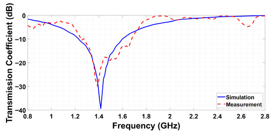
Figure 6.
Measured (red line) and simulated (blue line) transmission coefficient of the FSS panel for the passive shielding test-case.
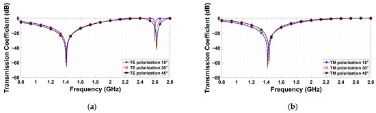
Figure 7.
Numerically obtained response of the passive FSS to varying incidence angles for both TE (a) and TM (b) polarizations.
3. Active Screen
Most daily activities depend on portable devices (smartphones, tablets) that handle personal data, which can be at risk if intercepted. While security measures like biometrics and encryption are in place, skilled attackers can exploit physical signals such as power consumption and spurious electromagnetic emissions to bypass these protections. Advances in Artificial Intelligence enable eavesdroppers to analyze large data quickly, making attacks more effective. One notable method, Screen Gleaning, involves extracting sensitive screen content through EM emissions without needing direct line of sight, and this technique could potentially be used against various devices [45,46].
3.1. Application Scenario
To propose a practical test case, the scenario presented in [45] was chosen for defining our screen properties. In that study, the experiments were conducted using some commonly available smartphones, whose screen specifications in terms of signal leakage are measured and claimed to be within the 150–465 MHz band. In this scope, a new unit cell geometry was investigated to develop an FSS shield intended to function as a stopband filter for blocking undesired electromagnetic emissions within the new operative frequency range. In addition, we confer an active nature to the proposed FSS solution, enabling the shielding capability to be switched on and off, allowing it to be activated solely in accordance with the user’s policy. Such functionality not only makes it possible to activate the shielding modality on demand, but also to exploit the switching capability as a means of information modulation.
3.2. Design and Realization of the FSS Active Panel
The FSS unit cell consists of four loops interconnected by three strips per side and fabricated from the same transparent conductive ITO film adopted also for the passive FSS design. Similarly, the substrate remains composed of two 60 cm × 60 cm glass layers, one above and one below to the FSS sheet, as illustrated in Figure 8a. The conservative optical transmittivity is 59%, as estimated for the passive scenario. All the geometrical parameters are listed in Table 3 and highlighted in Figure 8b. On the bottom surface of the lower glass layer, a biasing network is implemented to manage the active functionality of this configuration. Indeed, the unit cell functions as a filter by selectively attenuating electromagnetic waves within the 150–465 MHz frequency range, thereby effectively suppressing signals within this band while permitting the transmission of others. To achieve active control over the filtering characteristics, i.e., to switch between the filtering state and a radiofrequency-transparent state, the unit cell has been modified by introducing physical interruptions at specific locations, as illustrated in Figure 8b. At each of these breaks, an electrically controlled switch has been integrated using PIN diodes, as shown in Figure 9a. A suitable biasing network is designed to correctly polarize the PIN diodes by applying the appropriate DC voltage between their anode and cathode terminals, enabling the switching of their states. Implementing this functionality requires a significant modification of the FSS unit cell layout through the addition of the lower biasing layer, as represented in Figure 8a.
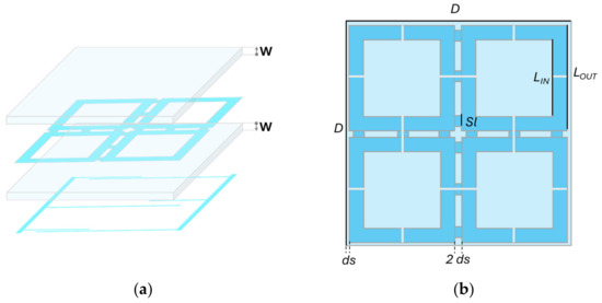
Figure 8.
Active shield unit cell description: (a) exploded view of the unit cell, (b) shape of the unit cell whose size and periodicity are listed in Table 3.
Table 3.
Geometrical dimensions of the active FSS panel.
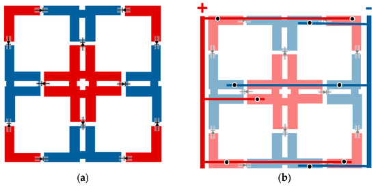
Figure 9.
Active panel management network: (a) positioning and orientation of the PIN diodes along the physical cuts, (b) biasing network used to control the switching operation on a single unit cell, with the vias represented as black dots. The red and the blue regions represent anodes and cathodes, respectively.
Based on the selected configuration for the cuts, the FSS unit cell is segmented into nine distinct regions interconnected by the diodes. Each region must be connected to either the positive or negative supply line according to a specific scheme, as illustrated in Figure 9a. To facilitate these connections, the bottom layer is perforated at each sub-region to accommodate conductive vias, which link the portions of the FSS unit cell above the glass layer to the biasing network located on the opposite side of the substrate. The vias have a radius of 0.6 mm. The biasing network consists of six 1 cm wide conductive strips that route the electrical connections from the vias to the positive or negative power lines, in accordance with the predetermined polarity assignments, Figure 9b. Finally, to decouple the RF signal from the DC generator, we added a 1 mH series inductor (LQH55DN102M03L, Murata Manufacturing Co., Ltd., Nagaokakyo, Japan) to each of the two output ports.
Given that the experiment is conducted at low frequencies and the unit cell periodicity is 30 cm—around one third of the wavelength at the center frequency (around 300 MHz)—the prototype is limited to a 2 × 2 array of unit cells, forming a square panel of 60 cm per side. This configuration is designed to facilitate the handling at the laboratory scale during the measurement campaign, as shown in Figure 10.
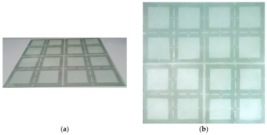
Figure 10.
Realization of the active shield integrated into a glass window 60 cm × 60 cm: (a) FSS layer before cutting, and (b) final screen after diodes integration. The panel is photographed on a white background to enhance the visibility of the ITO layers.
3.3. Performance Measurement
After completing the assembly of the active prototype with the same process followed for the passive panel, numerical simulations and experimental measurements were conducted to verify the ability of the reconfigurable metasurface to switch between its two operational states. For the numerical simulations, we adopted the same software and modeling conditions followed for the passive panel (Feko with periodic boundary conditions). Notably, the DC biasing network was incorporated into the numerical model to accurately account for any potential parasitic effects. Similarly, also the measurement setup is identical to that employed in the passive case, Figure 5b, with the addition of a DC signal generator used to bias the PIN diodes (GMP4215-GM1, Microchip Technology Inc., Chandler, AZ, USA). Since the primary focus is on emphasizing the switching behavior, the analysis was performed on the comparison of the transmission coefficients relating to the “ON” (τON) and “OFF” (τOFF) states. Both coefficients were evaluated as the difference between the S21 parameter measured when the “ON” (S21, ON) or “OFF” (S21, OFF) states are respectively imposed, and the S21 measured with no panel between the two antennas (S21, FS):
τON = 20∙log10 (S21, ON) − 20∙log10 (S21, FS),
τOFF = 20∙log10 (S21, OFF) − 20∙log10 (S21, FS).
Figure 11 illustrates the frequency-dependent experimental behavior in transmission between the “ON” and “OFF” states of the fabricated metasurface. For completeness, Figure 11 includes the transmission coefficient estimated from finite-array full-wave simulations, which are adopted as the reference model for the measurement configuration, as they accurately reproduce the antenna placement and finite-aperture conditions. The results were obtained by applying the time-gating technique to the measured signal [47,48]. Specifically, after performing the inverse Fourier transform on the frequency-domain data, a temporal window filter was applied to isolate only the direct contribution between the two antennas, removing components due to reflections or multipath propagation. The Fourier transform was then applied to return the filtered signal to the frequency domain, providing a more accurate characterization of the direct link. Both transmission coefficients exhibit negative values in logarithmic scale, as they have been normalized with respect to the direct connection. The direct connection arrangement, being measured without the panel, results in the highest value of coupling between the antennas. The data reveal an attenuation of more than 10 dB across the 150–500 MHz frequency band, indicating a significant reduction in signal transmission when the shielding is activated. Additionally, a pronounced attenuation feature is observed near 420 MHz, which is consistently observed in both measurements and simulations of the measurement scenario (near 465 MHz) and may be influenced by the applied time-domain gate filtering.” Conversely, the OFF state allows transmission within the desired band, while the observed insertion loss is mainly attributable to the intrinsic ohmic losses of the transparent ITO layer rather than to the FSS geometry itself, representing a trade-off required to achieve optical transparency and motivating further optimization of low-loss transparent conductive materials. These results collectively demonstrate the efficacy of the reconfigurable shield in selectively suppressing electromagnetic waves within the specified frequency range, validating the design and the active switching mechanism implemented in the prototype.
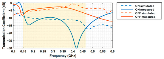
Figure 11.
Comparison of the transmission coefficients in the ON and OFF states of the active band-stop FSS designed for screen-gleaning prevention, including both simulated and measured results. The yellow highlighted region indicates the frequency range targeted in the filter design, corresponding to the intended suppression band.
4. Conclusions
In this paper, two different implementations of Frequency Selective Surfaces for EM-SCA prevention have been presented. In particular, in the passive configuration, the shielding of the undesired electromagnetic emission from the CPU of IoT device has been considered. The proposed FSS design achieved a maximum attenuation level of 30 dB and a −15 dB stopband of only 200 MHz, thus representing a substantial reduction in the signal at 1.4 GHz, while preserving the other wireless communication functionalities as Bluetooth and Wi-Fi. Compensating for such significant attenuation by merely increasing the receiving antenna’s gain is technically challenging and economically unfeasible in many practical scenarios. Therefore, a malicious eavesdropper attempting to intercept the signal would face a major obstacle, forcing them to physically approach the signal source, thus increasing the likelihood of detection.
On the other hand, in the active solution, the ability to switch on and off the protective shield for screen gleaning avoidance adds another layer of flexibility. Indeed, an internal signal source could be employed to modulate information, enabling covert communication with an authorized receiver, all while remaining undetected by potential intruders.
A significant advantage of both the implementations presented in this work lies in the fabrication, exploiting optically transparent materials. This characteristic opens a wide range of applications where traditional opaque shielding would hinder functionality or lead to a loss of crucial information. For example, in architectural settings, such as windows in sensitive environments, the ability to integrate transparent metasurfaces allows for secure electromagnetic shielding without compromising the visual or aesthetic qualities of the space. Although ITO-based solutions may entail a cost premium compared to simple metal sheets—particularly when accounting for glass integration—they uniquely enable the combination of electromagnetic shielding and optical transparency, which is not achievable with traditional opaque materials. Thus, the proposed transparent metasurfaces not only enhance security but also provide practical, unobtrusive solutions for a variety of real-world scenarios.
Author Contributions
Conceptualization, D.B.; methodology, P.U. and D.B.; validation, P.U., G.S. and D.B.; formal analysis, P.U. and D.B.; investigation, D.B.; visualization, P.U. and G.S.; writing—original draft preparation, P.U.; writing—review and editing, P.U., G.S., D.B. and A.M.; supervision, A.M. All authors have read and agreed to the published version of the manuscript.
Funding
This research received no external funding.
Institutional Review Board Statement
Not applicable.
Informed Consent Statement
Not applicable.
Data Availability Statement
The original contributions presented in this study are included in the article. Further inquiries can be directed to the corresponding author.
Acknowledgments
This research is partially supported by the Italian Ministry of University and Research (MUR) as part of the PNRR M4C2—HPC, Big data and Quantum Computing (Simulazioni, calcolo e analisi dei dati e altre prestazioni—CN1)—CUP I53C22000690001 SPOKE 6 Multiscale modelling & Engineering applications and in the framework of the FoReLab and CrossLab projects (Departments of Excellence).
Conflicts of Interest
The authors declare no conflicts of interest.
References
- Spence, A.; Bangay, S. Side-Channel Sensing: Exploiting Side-Channels to Extract Information for Medical Diagnostics and Monitoring. IEEE J. Transl. Eng. Health Med. 2020, 8, 1–13. [Google Scholar] [CrossRef] [PubMed]
- Lee, I. Internet of Things (IoT) Cybersecurity: Literature Review and IoT Cyber Risk Management. Future Internet 2020, 12, 157. [Google Scholar] [CrossRef]
- Agrawal, D.; Archambeault, B.; Rao, J.R.; Rohatgi, P. The EM Side-Channel(s). In Cryptographic Hardware and Embedded Systems—CHES 2002; Kaliski, B.S., Koç, Ç.K., Paar, C., Eds.; Springer: Berlin/Heidelberg, Germany, 2003; pp. 29–45. [Google Scholar] [CrossRef]
- Giechaskiel, I.; Rasmussen, K. Taxonomy and Challenges of Out-of-Band Signal Injection Attacks and Defenses. IEEE Commun. Surv. Tutor. 2020, 22, 645–670. [Google Scholar] [CrossRef]
- Kocher, P.; Jaffe, J.; Jun, B. Differential Power Analysis. In Advances in Cryptology—CRYPTO’99; Wiener, M., Ed.; Springer: Berlin/Heidelberg, Germany, 1999; pp. 388–397. [Google Scholar] [CrossRef]
- Gandolfi, K.; Mourtel, C.; Olivier, F. Electromagnetic Analysis: Concrete Results. In Cryptographic Hardware and Embedded Systems—CHES 2001; Koç, Ç.K., Naccache, D., Paar, C., Eds.; Springer: Berlin/Heidelberg, Germany, 2001; Volume 2162, pp. 251–261. [Google Scholar] [CrossRef]
- Goller, G.; Sigl, G. Side Channel Attacks on Smartphones and Embedded Devices Using Standard Radio Equipment. In Constructive Side-Channel Analysis and Secure Design; Mangard, S., Poschmann, A.Y., Eds.; Springer: Cham, Switzerland, 2015; pp. 255–270. [Google Scholar] [CrossRef]
- Standaert, F.-X.; Malkin, T.G.; Yung, M. A Unified Framework for the Analysis of Side-Channel Key Recovery Attacks. In Advances in Cryptology—EUROCRYPT 2009; Joux, A., Ed.; Springer: Berlin/Heidelberg, Germany, 2009; pp. 443–461. [Google Scholar] [CrossRef]
- Wang, R.; Wang, H.; Dubrova, E. Far Field EM Side-Channel Attack on AES Using Deep Learning. In Proceedings of the 4th ACM Workshop on Attacks and Solutions in Hardware Security (ASHES’20), Virtual, 13 November 2020; ACM: New York, NY, USA, 2020; pp. 35–44. [Google Scholar] [CrossRef]
- Spreitzer, R.; Moonsamy, V.; Korak, T.; Mangard, S. Systematic Classification of Side-Channel Attacks: A Case Study for Mobile Devices. IEEE Commun. Surv. Tutor. 2018, 20, 465–488. [Google Scholar] [CrossRef]
- Singh, A.; Kar, M.; Mathew, S.K.; Rajan, A.; De, V.; Mukhopadhyay, S. Improved Power/EM Side-Channel Attack Resistance of 128-Bit AES Engines with Random Fast Voltage Dithering. IEEE J. Solid-State Circuits 2019, 54, 569–583. [Google Scholar] [CrossRef]
- Fan, J.; Guo, X.; De Mulder, E.; Schaumont, P.; Preneel, B.; Verbauwhede, I. State-of-the-Art of Secure ECC Implementations: A Survey on Known Side-Channel Attacks and Countermeasures. In Proceedings of the IEEE International Symposium on Hardware-Oriented Security and Trust (HOST), Anaheim, CA, USA, 13–14 June 2010; IEEE: Washington, DC, USA, 2010; pp. 76–87. [Google Scholar] [CrossRef]
- Lyu, Y.; Mishra, P. A Survey of Side-Channel Attacks on Caches and Countermeasures. J. Hardw. Syst. Secur. 2018, 2, 33–50. [Google Scholar] [CrossRef]
- Wu, Z.; Ding, L.; Li, Z.; Wang, X.; Guan, Z. Side Channel Attacks on GPRS Standard Encryption Algorithms. ACM Trans. Embed. Comput. Syst. 2025, 24, 1–16. [Google Scholar] [CrossRef]
- Usai, P.; Brizi, D.; Monorchio, A. Low Frequency Magnetic Metasurface for Wireless Power Transfer Applications: Reducing Losses Effect and Optimizing Loading Condition. IEEE Access 2023, 11, 66579–66586. [Google Scholar] [CrossRef]
- Li, H.; Feng, Y.; Zhao, M.; Wang, X.; Brizi, D.; Fang, X.; Hu, J.; Sima, B.; Zong, Z.; Wu, W.; et al. A Dual-Polarized and Wideband Switchable Absorption/Transmission Frequency Selective Surface with Multispectral Functionality. IEEE Open J. Antennas Propag. 2024, 5, 286–296. [Google Scholar] [CrossRef]
- Engheta, N.; Ziolkowski, R.W. Metamaterials: Physics and Engineering Explorations; IEEE Press: Piscataway, NJ, USA; Wiley-Interscience: Hoboken, NJ, USA, 2006. [Google Scholar]
- Veselago, V.G. The Electrodynamics of Substances with Simultaneously Negative Values of ε and μ. Phys. Usp. 1968, 10, 509–514. [Google Scholar] [CrossRef]
- Ott, R.H.; Kouyoumjian, R.G.; Peters, L. Scattering by a Two-Dimensional Periodic Array of Narrow Plate. Radio Sci. 1967, 2, 1347–1359. [Google Scholar] [CrossRef]
- Mittra, R.; Chan, C.C.; Cwik, T. Technique for Analyzing Frequency Selective Surfaces (FSS)—A Review. Proc. IEEE 1988, 76, 1593–1615. [Google Scholar] [CrossRef]
- Munk, B.A. Frequency Selective Surfaces: Theory and Design; John Wiley & Sons: Hoboken, NJ, USA, 2005. [Google Scholar]
- Aboualalaa, M.; Pokharel, R.K. In Vitro Demonstration of Battery Charging Using Compact Four-Resonator WPT System with Stacked Metamaterial for Biomedical Implants. IEEE Trans. Microw. Theory Tech. 2025, 73, 9173–9186. [Google Scholar] [CrossRef]
- Müller, J.; Falchi, M.; Stoja, E.; Konstandiri, S.; Gunther, M.; Brizi, D.; Usai, P.; Monorchio, A.; Philipp, D. Deep-Learning Optimized Reconfigurable Metasurface for Magnetic Resonance Imaging. In Proceedings of the 18th European Conference on Antennas and Propagation (EuCAP), Glasgow, UK, 17–22 March 2024; IEEE: Berlin, Germany, 2024. [Google Scholar] [CrossRef]
- Yang, J.; Li, Y.; Guo, J.; Wu, Z.; Tang, M.-C. A Compact, Broadband, Radar-Infrared Multispectral Stealth Antenna Based on Dual-Functional Polarization Conversion Metasurface. IEEE Trans. Antennas Propag. 2025, 73, 7057–7062. [Google Scholar] [CrossRef]
- Hakim, M.L.; Alam, T.; Islam, M.T. Polarization-Insensitive and Oblique Incident Angle Stable Miniaturized Conformal FSS for 28/38 GHz mm-Wave Band 5G EMI Shielding Applications. IEEE Antennas Wirel. Propag. Lett. 2023, 22, 2644–2648. [Google Scholar] [CrossRef]
- De Mello, R.G.L. Metasurface-Driven Electronic Warfare; IEEE eBooks: New York, NY, USA, 2025; Available online: https://ieeexplore.ieee.org/book/10799164 (accessed on 16 September 2025).
- Kim, M.-S.; Kim, S.-S. Design and Fabrication of 77-GHz Radar Absorbing Materials Using Frequency-Selective Surfaces for Autonomous Vehicles Application. IEEE Microw. Wirel. Compon. Lett. 2019, 29, 779–782. [Google Scholar] [CrossRef]
- Violi, V.; Brizi, D.; Monorchio, A. Multi-Layer Frequency Selective Surface Wideband Filter with High Selectivity Operating in L, S, and C Bands. Sci. Rep. 2025, 15, 26988. [Google Scholar] [CrossRef]
- Li, Y.; Ren, P.; Xiang, Z.; Xu, B.; Chen, R. Design of Dual-Stopband FSS with Tightly Spaced Frequency Response Characteristics. IEEE Microw. Wirel. Compon. Lett. 2022, 32, 1011–1014. [Google Scholar] [CrossRef]
- Falchi, M.; Masi, A.; Usai, P.; Monorchio, A.; Brizi, D. An Electronically Reconfigurable Magnetic Metasurface for Enhanced Low-Frequency Wireless Power Transfer Applications. IEEE J. Microw. 2025, 5, 312–321. [Google Scholar] [CrossRef]
- Dellabate, A.; Lazzoni, V.; Monorchio, A.; Brizi, D. Arbitrarily Conformal Metasurfaces for Enhanced Wireless Power Transfer Systems. IEEE Access 2024, 12, 64376–64384. [Google Scholar] [CrossRef]
- Ferreira, D.; Sismeiro, L.; Ferreira, A.; Caldeirinha, R.F.S.; Fernandes, T.R.; Cuiñas, I. Hybrid FSS and Rectenna Design for Wireless Power Harvesting. IEEE Trans. Antennas Propag. 2016, 64, 2038–2042. [Google Scholar] [CrossRef]
- Fatima, F.; Akhtar, M.J.; Ramahi, O.M. Frequency Selective Surface Structures-Based RF Energy Harvesting Systems and Applications. IEEE Microw. Mag. 2024, 25, 47–69. [Google Scholar] [CrossRef]
- Payne, K.; Xu, K.; Choi, J.H. Generalized Synthesized Technique for the Design of Thickness Customizable High-Order Bandpass Frequency-Selective Surface. IEEE Trans. Microw. Theory Tech. 2018, 66, 4783–4793. [Google Scholar] [CrossRef]
- Roberts, J.; Ford, K.L.; Rigelsford, J.M. Secure Electromagnetic Buildings Using Slow Phase-Switching Frequency-Selective Surfaces. IEEE Trans. Antennas Propag. 2016, 64, 251–261. [Google Scholar] [CrossRef]
- Rajendran, S.; Sun, Z.; Lin, F.; Ren, K. Injecting Reliable Radio Frequency Fingerprints Using Metasurface for the Internet of Things. IEEE Trans. Inf. Forensics Secur. 2021, 16, 1896–1911. [Google Scholar] [CrossRef]
- Decoster, B.; Maes, S.; Cuiñas, I.; García Sánchez, M.; Caldeirinha, R.; Verhaevert, J. Dual-Band Single-Layer Fractal Frequency Selective Surface for 5G Applications. Electronics 2021, 10, 2880. [Google Scholar] [CrossRef]
- Cuiñas, I.; Expósito, I.; Andriukaitis, D.; Caldeirinha, R.F.S.; García Sánchez, M.; Valinevičius, A. Integration of Frequency-Selective Surfaces as Smart Skins in Building Envelopes and Divisions: Insulation and Energy Issues. World 2024, 5, 62. [Google Scholar] [CrossRef]
- Vásquez-Peralvo, J.A.; Fernández-González, J.M.; Rigelsford, J.M.; Valtr, P. Interwoven Hexagonal Frequency Selective Surface: An Application for WiFi Propagation Control. IEEE Access 2021, 9, 111552–111566. [Google Scholar] [CrossRef]
- Liang, J.C.; Gao, Y.; Cheng, Z.W.; Jiang, R.Z.; Dai, J.Y.; Zhang, L.; Cheng, Q.; Cui, T.J. An optically transparent reconfigurable intelligent surface with low angular sensitivity. Adv. Opt. Mater. 2024, 12, 2202081. [Google Scholar] [CrossRef]
- Kitayama, D.; Hama, Y.; Goto, K.; Miyachi, K.; Motegi, T.; Kagaya, O. Transparent dynamic metasurface for a visually unaffected reconfigurable intelligent surface: Controlling transmission/reflection and making a window into an RF lens. Opt. Express 2021, 29, 29292–29307. [Google Scholar] [CrossRef]
- Deng, M.; Cui, T.; Hou, B.; Zhang, Y.; Zhao, H.; Jiang, H.; Yin, L.; Gong, C.; Fan, F.; Chang, S. Mesh-based metasurfaces with high optical transparency. Opt. Express 2025, 33, 49380–49392. [Google Scholar] [CrossRef]
- Sayakkara, A.; Le-Khac, N.-A.; Scanlon, M. Leveraging Electromagnetic Side-Channel Analysis for the Investigation of IoT Devices. Digit. Investig. 2019, 29, S94–S103. [Google Scholar] [CrossRef]
- PCD Antenna—Precision Conical Dipole Antenna. Available online: https://rf.seibersdorf-laboratories.at/fileadmin/uploads/intranet/dateien/folder/produktblatt_le_pcd_en_web.pdf (accessed on 16 September 2025).
- Liu, Z.; Samwel, N.; Weissbart, L.; Zhao, Z.; Lauret, D.; Batina, L.; Larson, M. Screen Gleaning: A Screen Reading TEMPEST Attack on Mobile Devices Exploiting an Electromagnetic Side Channel. In Proceedings of the Network and Distributed Systems Security (NDSS) Symposium 2021, Virtual, 21–25 February 2021; Internet Society: Fredericksburg, VA, USA, 2021. [Google Scholar] [CrossRef]
- Sun, D.-G.; Shi, J.; Wei, D.; Zhang, M. Method for Detecting Text Information Leakage in Electromagnetic Radiation from a Computer Display. IET Inf. Secur. 2016, 10, 413–417. [Google Scholar] [CrossRef]
- Soltane, A.; Andrieu, G.; Perrin, E.; Decroze, C.; Reineix, A. Antenna Radiation Pattern Measurement in a Reverberating Enclosure Using the Time-Gating Technique. IEEE Antennas Wirel. Propag. Lett. 2020, 19, 183–187. [Google Scholar] [CrossRef]
- Koh, J.; De, A.; Sarkar, T.K.; Moon, H.; Zhao, W.; Salazar-Palma, M. Free-Space Radiation Pattern Reconstruction from Non-Anechoic Measurements Using an Impulse Response of the Environment. IEEE Trans. Antennas Propag. 2012, 60, 821–831. [Google Scholar] [CrossRef]


Disclaimer/Publisher’s Note: The statements, opinions and data contained in all publications are solely those of the individual author(s) and contributor(s) and not of MDPI and/or the editor(s). MDPI and/or the editor(s) disclaim responsibility for any injury to people or property resulting from any ideas, methods, instructions or products referred to in the content. |
© 2026 by the authors. Licensee MDPI, Basel, Switzerland. This article is an open access article distributed under the terms and conditions of the Creative Commons Attribution (CC BY) license.