Abstract
Nanoparticle floating gate (NPFG) transistors have gained attention as synaptic devices due to their discrete charge storage capability, which minimizes leakage currents and enhances the memory window. In this study, we propose and evaluate a mesh-type floating gate transistor (Mesh-FGT) designed to emulate the characteristics of NPFG transistors. Individual floating gates with dimensions of 3 µm × 3 µm are arranged in an array configuration to form the floating gate structure. The Mesh-FGT is composed of an Al/Pt/Cr/HfO2/Pt/Cr/HfO2/SiO2/SOI (silicon-on-insulator) stack. Threshold voltages (Vth) extracted from the transfer and output curves followed Gaussian distributions with means of 0.063 V (σ = 0.100 V) and 1.810 V (σ = 0.190 V) for the erase (ERS) and program (PGM) states, respectively. Synaptic potentiation and depression were successfully demonstrated in a multi-level implementation by varying the drain current (Ids) and Vth. The Mesh-FGT exhibited high immunity to leakage current, excellent repeatability and retention, and a stable memory window that initially measured 2.4 V. These findings underscore the potential of the Mesh-FGT as a high-performance neuromorphic device, with promising applications in array device architectures and neuromorphic neural network implementations.
1. Introduction
The rapid growth of information in recent years has highlighted the limitations of existing systems in efficiently processing large datasets, prompting the exploration of various technological solutions [,,]. Traditional von Neumann computing architectures, which transfer data between memory and the central processing unit (CPU), offer versatility and practicality. However, the von Neumann architecture is limited by a memory bus bandwidth bottleneck, which slows data transfer between memory and the CPU, particularly during sequential processing for memory updates [,].
To address these limitations, neuromorphic devices have emerged as a promising alternative by configuring neural networks directly in hardware. Neuromorphic devices emulate biological neurons and synapses through mechanisms like spike-based signaling and synaptic weight adjustment, enabling parallel processing operations with low power consumption and high speed [,,].
Typical neuromorphic devices include memristors and field-effect transistors (FETs) [,,,,]. Memristors, developed in various forms such as resistive random-access memory (RRAM), phase-change random-access memory (PCRAM), and magnetic random-access memory (MRAM), are considered promising synaptic devices due to their simple structure and suitability for crossbar array (CBA) architectures []. However, CBA structures suffer from sneak currents, where current flows in undesired directions, necessitating the integration of three-terminal structures to mitigate these issues. Furthermore, achieving long-term reliability remains challenging due to the degradation of resistance states over time.
In contrast, FETs offer precise control of current flow through gate voltage modulation, effectively eliminating sneak path issues. Additionally, their standardized manufacturing processes facilitate large-scale production and integration. Flash transistors, characterized by non-volatile behavior, can emulate synapses by implementing learning and memory functions through output signal modulation via floating gates [,,,].
Among floating gate devices, nanoparticle floating gate (NPFG) structures have been developed with a focus on discrete charge trapping. NPFG transistors exhibit superior durability, low power consumption, and multi-level capability compared to continuous (conventional) floating gate transistors. Materials such as gold, quantum dots, aluminum and silicon carbide are employed as nanoparticles, with their charge storage capacity tunability based on material type, size, and density, enabling extensive comparative analyses [,,,,,]. In our previous work, we developed an NPFG device using InP quantum dots and demonstrated excellent performance []. However, the non-uniform size and dispersion of quantum dots adversely affect carrier mobility and device reproducibility, and their low thermal stability further compromises device stability at high temperatures. [,].
In this study, to address these limitations, the uniform size and dispersion of the floating gate were controlled through photolithography, and the limitations of NPFG were addressed by utilizing platinum, which exhibits high thermal stability.
In addition, by ensuring spatial uniformity and structural precision of the charge storage locations, this work aims to implement a synaptic device with high reproducibility.
This structure presents a unique approach not discussed in the previous literature, namely the regularized spatial control of charge storage regions, and it is meaningful in that it considers both scalability to nanoscale structures and expandability to neuromorphic array architectures. The minimum pattern size achievable using a contact aligner (i-line, 365 nm) was set to 3 μm × 3 μm for each floating gate, which was implemented in a mesh-type arrangement. The detailed structures, processes, and their electrical characteristics are discussed in subsequent sections.
The structure of this paper is organized as follows: In Section 2, we provide a detailed explanation of the experimental methods, including the device structure of the Mesh-FGT, the fabrication process, and the measurement conditions. Section 3 presents the experimental results, such as the program/erase (PGM/ERS) operations identified through electrical characterization, synaptic weight modulation depending on threshold voltage and drain current, and retention characteristics. In Section 4, we discuss the device operation mechanism and its technical significance based on the experimental results and analyze the advantages of the mesh-type structure in terms of reproducibility compared to conventional NPFG devices. Finally, Section 5 summarizes the overall conclusions of this study and suggests future research directions for the structural scalability of the device and its application to neuromorphic systems.
2. Materials and Methods
The fabrication process of the device is shown in Figure 1a. A silicon-on-insulator (SOI) wafer is utilized to minimize electron interactions between devices and reduce leakage current. After cleaning the SOI wafer, unnecessary silicon regions were removed through an etching process, and each device was fabricated in an isolated form on top of the BOX layer. By utilizing the insulating BOX layer of the SOI structure, each device is electrically isolated from the underlying substrate, enabling accurate electrical characterization without interference between devices. The SOI wafer consists of a device (silicon) layer with a resistivity of 8–22 Ω·cm and a thickness of 290 nm, a buried oxide (BOX) layer with a thickness of 1 μm, and a substrate layer with a thickness of 675 μm.
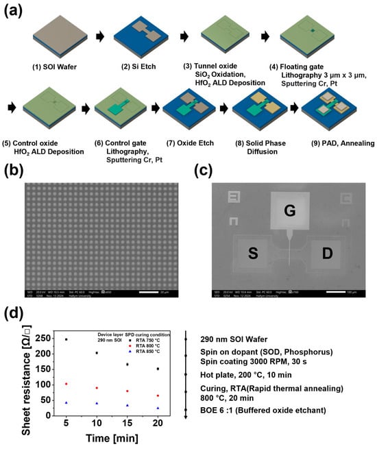
Figure 1.
(a) Schematic diagram of device fabrication. SEM image of (b) mesh-type floating gate and (c) Mesh-FGT. (d) The SPD process and a comparison of sheet resistance based on RTA temperature and curing time.
The fabrication process starts with cleaning procedure using acetone, methanol, SPM (sulfuric peroxide mixture), and BOE (buffered oxide etchant, 6:1) solutions. Subsequently, lithography and etching processes are conducted to define the active area. The tunnel oxide, which facilitates electron tunneling, is fabricated by forming a 30 Å thick SiO2 layer using thermal dry oxidation in a furnace, followed by the deposition of 50 cycles HfO2 using atomic layer deposition (ALD) method.
The floating gate, serving as the electron storage and erase site, is implemented in a mesh-type structure using chromium (Cr) and platinum (Pt). Image reversal lithography (IR lithography) is employed to pattern the mesh-type floating gates by optimizing UV exposure and development times []. A total of 2.5 nm of Cr and 25 nm of Pt are deposited via sputtering, and the mesh pattern is defined using a lift-off process to complete the floating gate. As shown in Figure 1b, the mesh-type floating gate is fabricated with dimensions of 3 μm × 3 μm, acting as separated floating charge storage node under the control gate. We fabricate the mesh-type floating gate due to its durability and multi-level functionality.
The control oxide, which acts as a barrier to prevent electron erasure from the floating gate, is designed to be thicker than the tunnel oxide. This layer was fabricated by depositing 200 cycles of HfO2 using ALD process. The control gate is then formed by depositing 2.5 nm of Cr and 100 nm of Pt, followed by IR lithography, sputtering, and lift-off processes. Figure 1c shows the SEM image of the manufactured synaptic device with a gate width of 50 μm and a gate length of 3 μm, respectively.
Before n-type phosphorus doping, an etching process is conducted to remove deposited HfO2 and oxidized SiO2 in the areas designated for dopant injection. Phosphorus is subsequently introduced into the device using the solid phase diffusion (SPD) process [,,]. Figure 1d shows a schematic of the SPD process and a comparison of sheet resistance according to the temperature and time of RTA (rapid thermal annealing) during the curing process. The RTA temperature and time are chosen as the optimal process conditions to minimize control gate damage and to satisfy a doping concentration of 1019 cm−3 or higher. At an RTA temperature of 800 °C and a duration of 20 min, sheet resistance is measured as 65 Ω/□ and the doping concentration is determined to be 5 × 1019 cm−3 using the four-point probe system and the Hall effect measurement system.
To enhance electrical contact between the probe and the source, drain, and gate during device measurements, the Al pad formation process is performed using IR lithography, sputtering, and lift-off techniques. Finally, an annealing process is performed in a box furnace at 450 °C for 1 h to reduce overall device resistance and restore the crystal structure, completing the device fabrication. All processes were conducted in the cleanroom facility at the Nano Fab of Hallym University.
The electrical performance of the fabricated device was evaluated using the B1500A Semiconductor Device Parameter Analyzer (Keysight Technologies, Santa Rosa, CA, USA), with probes connected to the gate, source, drain, and substrate. The measurement software used was Keysight EasyEXPERT (version 6.4.2312.1715), and the collected data were analyzed and visualized using Microsoft Excel (version 2506) and OriginLab Origin (version 8.5).
Table 1 presents the voltage conditions applied during the program (PGM) and erase (ERS) operations. In this study, to effectively represent synaptic weight, the PGM and ERS operations were each repeated 20 times. During the 20-cycle experiment, the ERS operation was conducted by applying a gate voltage (Vgs) of −6 V for 10 s. Additionally, the substrate voltage (Vsub) was incrementally increased by 1 V per cycle, ranging from 1 V to 20 V, for a total of 20 repetitions. The source voltage (Vss) and drain voltage (Vds) were maintained at 0 V throughout this process. Conversely, the PGM operation was conducted by applying Vgs of 6 V. This voltage was applied twice at 1 s intervals, increasing from 1 s to 10 s, resulting in a total of 20 repetitions. Throughout this process, Vsub, Vss, and Vds were maintained at 0 V.

Table 1.
Voltage applied during program and erase operations. All figures perform operations according to the following table.
3. Results
The fundamental operation of the device is analyzed through transfer curves and output curves. In Figure 2a,b, the threshold voltage (Vth) is calculated from the transfer curves and the corresponding transconductance (gm) with Vds of 0.1 V applied [,]. The Vth in the ERS state was about 0.03 V, while in the PGM state, it was about 1.8 V. The subthreshold swing (SS) was calculated as 113 mV/decade for the ERS state and 110 mV/decade for the PGM state. The device incorporates a composite dielectric layer (HfO2/SiO2) and a mesh-type floating gate structure, which result in a measured SS higher than the theoretical limit of 60 mV/decade due to factors such as interface traps and electric field non-uniformity. This increase in SS is interpreted as being caused by structural characteristics of the flash memory device and defects introduced during the fabrication process. Figure 2c shows the output curve for the ERS state, revealing a cut-off region at Vgs of 0 V and a saturation region between 1 and 5 V. Figure 2d illustrates the output curve for the PGM state, showing cut-off regions at Vgs = 0 V and Vgs = 1 V, with saturation confirmed from 2 to 5 V. The gate leakage current ranged from 10−13 A/μm to 10−11 A/μm for both the ERS state and the PGM state, demonstrating excellent insulation properties and suppression of leakage current, as shown in Figure 2e,f.
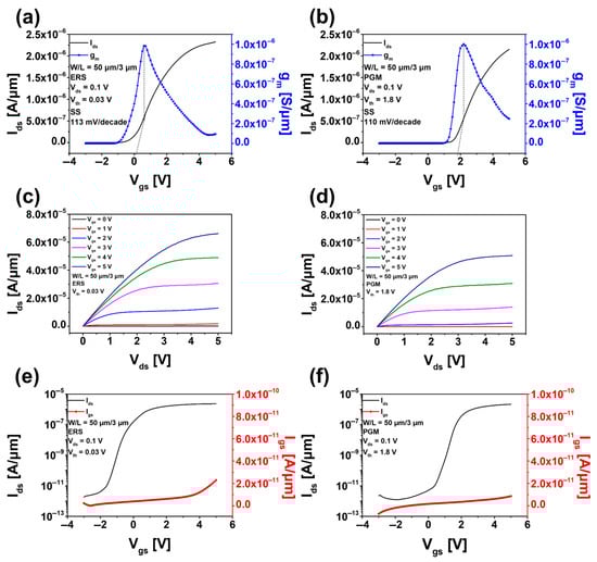
Figure 2.
Basic operation through transfer curves and output curves. Threshold voltage calculation of (a) full erase state and (b) full program state. Output curve of (c) full erase state and (d) full program state. Gate leakage current measurement of (e) full erase state and (f) full program state.
To verify the stable operation of the Mesh-FGT under appropriate voltage conditions, the channel mobility and Fowler–Nordheim (F–N) tunneling characteristics were evaluated. First, based on the transfer curve shown in Figure 2a, the channel mobility of the Mesh-FGT was calculated. Since the device operates in the linear region at Vds = 0.1 V, the channel mobility satisfies the following Equation (1):
: channel mobility [units: m2/V∙s or cm2/V∙s];
: oxide capacitance per unit area [units: F/m2];
: channel length [units: m];
: channel width [units: m];
: drain voltage [units: V];
: slope of Ids–Vgs curve [units: S = A/V].
Here, is 3 μm (3 × 10⁻⁶ m), and is 50 μm (50 × 10−6 m). The value of corresponds to the peak point of the mutual conductance (, which is calculated as 9.8236 × 10⁻⁷ S/μm × 50 μm = 4.9118 × 10⁻⁵ S. To determine the oxide capacitance (), which is a variable in the channel mobility equation, Figure 3a,b were utilized. Figure 3a shows the stack structure used to extract , which shares the same configuration and conditions as the fabricated Mesh-FGT device. Based on this structure, the capacitance–voltage curve was measured using an Agilent 4284A LCR Meter (Keysight Technologies, Santa Rosa, CA, USA), as shown in Figure 3b, and was calculated to be 1.508 × 10⁻¹⁰ F. Given that the electrode area is 200 μm × 200 μm, the areal capacitance is 3.77 × 10⁻³ F/m2. Consequently, the channel mobility () is calculated to be 0.007817 m2/V·s, which corresponds to 78.17 cm2/V·s. This value is within the typical range reported for similar devices, suggesting that the Mesh-FGT operates with stable electrical performance.
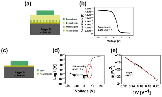
Figure 3.
Measurement results for evaluating oxide capacitance () and Fowler–Nordheim (F–N) tunneling characteristics. (a) Stack structure used for extracting . (b) Capacitance–voltage curve for extraction. (c) Stack structure for F–N tunneling analysis. (d) Log I-V curve (e) ln(I/V2) − 1/V curve.
Figure 3c–e illustrate the Fowler–Nordheim (F–N) tunneling characteristics of the Mesh-FGT and provide insight into the operating voltages for the program (PGM) and erase (ERS) operations. In a flash transistor, the charge stored in the floating gate modulates the channel conductivity by shifting the Vth. This charge is injected or removed through F–N tunneling during the PGM and ERS operations. The stack structure shown in Figure 3c served as the basis for the F–N tunneling evaluation, with Figure 3d,e presenting the corresponding electrical measurements. From the log I–V curve in Figure 3d, it can be observed that F–N tunneling occurs between 4.9 V and 8 V. Beyond this range, dielectric breakdown is evident. This implies that the PGM and ERS operations are feasible within this voltage window, while voltages outside this range are likely to result in device failure or non-operation. Figure 3e, along with the following F–N tunneling Equation (2), was used to closely examine whether the voltage range from 4.9 V to 8 V corresponds to the expected F–N tunneling behavior.
: tunnel oxide thickness [units: m];
: effective mass of electron [units: kg];
: barrier height [units: eV or J];
: Planck’s constant [units: J·s].
From the linear fitting, a negative slope of –80.27 was obtained within the specified voltage range, confirming that the data follows the proportional relationship characteristic of F–N tunneling. Therefore, it can be concluded that the dominant charge transport mechanism in the device is Fowler–Nordheim tunneling. Furthermore, the operating voltages listed in Table 1 (PGM: +6 V, ERS: –6 V) are within a stable range that does not induce dielectric breakdown, indicating reliable device operation.
The synaptic weight of the device is examined by analyzing the changes in Vth and drain current (Ids) during ERS and PGM operations. During ERS, the increase in current indicates synaptic potentiation, while the decrease in current during PGM reflects synaptic depression []. These phenomena are attributed to Fowler–Nordheim (F–N) tunneling, suggesting stable device operation [,]. Figure 4a,b demonstrate multi-level synaptic potentiation and depression over 40 cycles, with clear Vth changes. Figure 4c shows that the synaptic connection strength can be adjusted from −0.02 to 2.14 V, highlighting the potential of this device as an artificial synapse. In particular, a noticeable Vth shift is observed during the first PGM and ERS operations, which is attributed to the long voltage pulse duration (1~10 s) that induces significant initial charge injection and removal in the floating gate. To improve control over gradual synaptic weight changes, future experiments will adopt microsecond-scale pulse measurements using the B1500A system. The distribution of Vth was analyzed using Figure 4d, confirming that it follows a Gaussian distribution [,,]. For the ERS state, we can see that the changes in Vth were smaller than for the PGM state, indicating a more centralized distribution. This suggests that the Vth in the ERS state exhibits better reproducibility compared to the PGM state. The Vth in the ERS state exhibited a Gaussian distribution with a mean (μ) of 0.063 V and a standard deviation (σ) of 0.100 V. In the PGM state, the Vth showed a mean of 1.810 V with a standard deviation of 0.190 V. The broader Vth variation in the PGM state is attributed to charge trapping during repeated operations. Additionally, since PGM was performed after full erase measurements, prior stress may have further degraded Vth reproducibility.
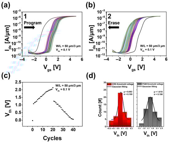
Figure 4.
(a) Synaptic potentiation and (b) synaptic depression at a drain voltage of 0.1 V. (c) Measurement of synaptic weights by threshold voltage. (d) Gaussian distribution in full erase states and full program states, based on threshold voltage.
Based on the transfer curves shown in Figure 4a,b, synaptic weights were extracted by analyzing the changes in Ids with respect to different read voltage (Vread) values. The corresponding results are depicted as black curves in Figure 5. The Vread is adjusted to ensure accurate data retrieval by setting a specific Vgs as the reference voltage. In this study, specific values of Vread values (0, 0.5, 1, and 1.5 V) were selected, and the synaptic weights were plotted based on the resulting changes in Ids, as illustrated in Figure 4.
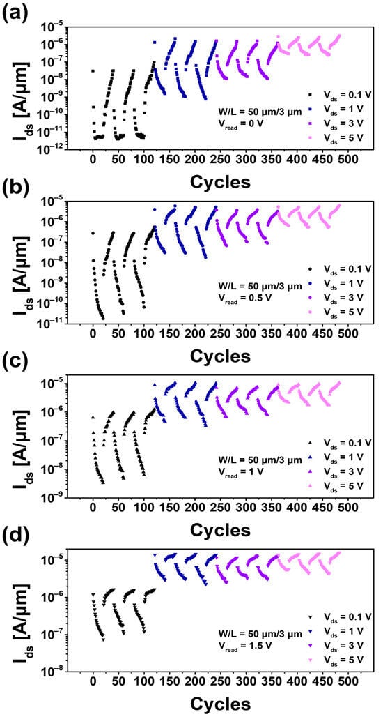
Figure 5.
Repeatability, a characteristic of device behavior. Synaptic weight analysis and repeatability evaluation based on drain voltage values (0.1, 1, 3, and 5 V) at read voltage (=Vgs) values of (a) 0, (b) 0.5, (c) 1, and (d) 1.5 V, respectively.
The long-term objective of this research is to develop synaptic array devices. Achieving this requires not only sufficient Ids but also significant synaptic weight variation. Therefore, in this study, synaptic weights were analyzed under various conditions by incorporating Vds as an additional variable alongside Vread, with the results presented in Figure 5. Furthermore, to assess the reliability of the device, its repeatability was evaluated by performing three program/erase (P/E) cycles.
To evaluate synaptic weight based on changes in Ids, appropriate Vds and Vread are selected []. Vds values were set to 0.1, 1, 3, and 5 V, taking into account the device characteristics, while Vread values were set to 0, 0.5, 1, and 1.5 V to ensure stable signal acquisition under various conditions.
A total of 484 repeated measurements (121 cycles × 4) were conducted using the initial Ids as a baseline for each combination of Vds and Vread. These measurements confirmed that the device accurately represents synaptic potentiation and depression. During repeated measurements, the device demonstrated stable current changes and maintained synaptic connection strength, even after hundreds of cycles. This indicates high durability and reliability, making the device suitable for neuromorphic array designs.
The subsequent goal of this study is to develop neuromorphic array devices capable of dynamically controlling signal transduction between neurons. To achieve this, the properties of a single synaptic device were examined. Under conditions where Vds = 1 V and Vread = 0.5 V, the device exhibited stable signal transmission and reading characteristics without degradation of synaptic connection strength. The results successfully demonstrated a synaptic current change of more than 103 times.
In neuromorphic array devices, the ability to perform parallel operations and respond to diverse input signals with multi-level synaptic connection strengths is critical. Therefore, stable and sufficiently high synaptic variation and current values are essential requirements. High synaptic variation precisely controls various signal strengths and effectively emulates the behavior between neurons and synapses. In addition, maintaining sufficiently high current prevents loss of synaptic connection strength, thereby improving signal transmission and ensuring device stability.
Figure 6 illustrates results from additional measurements under identical conditions (Vds = 1 V, Vread = 0.5 V), showing synaptic weights expressed as changes in Vth and Ids. The analysis of Vth reveals a change of 1.721 V, ranging from 0.186 V to 1.907 V. For changes in Ids, the synaptic weights can be precisely adjusted by more than 103 times, ranging from 10−9 A/μm to 10−6 A/μm, without compromising connection strength. This demonstrates the device’s strong potential for application in future array designs.
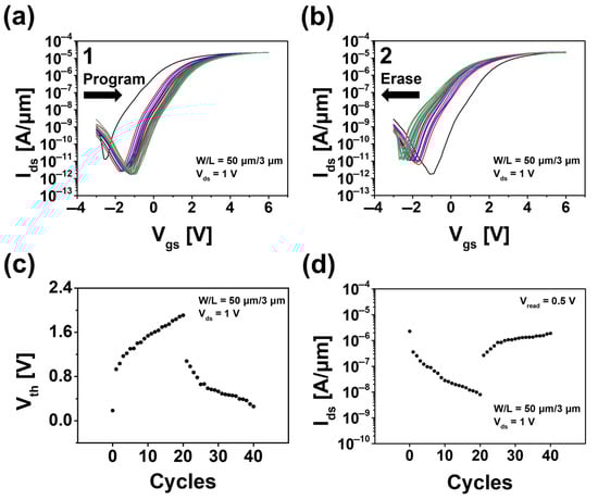
Figure 6.
(a) Synaptic potentiation and (b) synaptic depression at a drain voltage of 1 V. Measurement of synaptic weights by (c) threshold voltage and (d) drain current (Vds = 1 V, Vread = 0.5 V).
The retention characteristics of the device were analyzed under these operating conditions []. The device’s maximum synaptic potentiation and depression values were evaluated by transfer curves, and changes in the memory window were monitored over a period of 2880 min for each operation. Figure 7a shows the changes in Vth over 2880 min. During synaptic potentiation, Vth increased from –0.2 to 0.13 V, while during synaptic depression it decreased from 2.2 to 1.93 V, resulting in a memory window ranging from approximately 2.4 V to 1.8 V. Figure 7b shows the corresponding Ids changes over the same period, indicating that a stable current is maintained around 10−10 to 10−6 A/μm. The retention characteristics presented in this study were measured over a period of two days (2880 min) for both fully programmed and erased states. However, this does not imply that the device operates only for two days. The measurement duration was determined by time constraints associated with the use of the B1500A measurement system in the university cleanroom. As shown in Figure 6, after an initial fluctuation within approximately the first 180 min, both Vth and Ids remained stable. This trend aligns with the typical retention behavior of non-volatile memory devices. In future work, long-term retention characteristics over several weeks to months will be investigated.
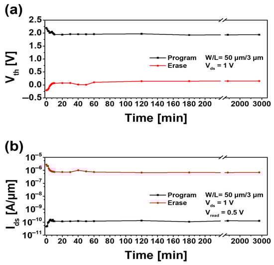
Figure 7.
Retention, a characteristic of device behavior. Two days of changes in (a) threshold voltage and (b) drain current.
Based on the retention results, gradual changes in Vth and Ids over time suggest that increasing the thickness of the control oxide film and implementing additional passivation layers would be necessary to prevent electron loss from the floating gate [,]. These modifications could further improve device stability and reproducibility.
4. Discussion
Previous studies on NPFG transistors have demonstrated advantages such as multi-level synaptic weight representation and an extended memory window. The NPFG device previously fabricated by our group also exhibited comparable performance []. However, it faced limitations in terms of reproducibility. The primary factors contributing to reduced reproducibility are the non-uniform distribution of nanoparticles (NPs) and the challenges associated with size control. To address these issues, this study proposes Mesh-FGT to achieve a more uniform floating gate pattern.
In the proposed structure, individual floating gates with dimensions of 3 μm × 3 μm were arranged in a mesh pattern using a contact aligner, facilitating uniform pattern formation. Furthermore, the size of the floating gates can be readily adjusted through a fabrication process involving IR lithography, sputtering, and lift-off techniques. The memory window was observed to be 2.4 V initially and sustained a value above 1.8 V over a duration of 2880 min.
Despite these advancements, the present design has certain limitations. The individual floating gates implemented in this study have a dimension of approximately 3 μm × 3 μm, posing challenges in forming an effective mesh pattern in transistors at the nanometer scale. Moreover, the current architecture is based on a single transistor, limiting its scalability for neuromorphic applications that require large-scale parallel computation.
To overcome these limitations, future research will proceed in two main directions:
First, future work will focus on reducing the size of individual floating gates to the nanometer scale. Specifically, a 10 nm × 10 nm floating gate mesh structure will be fabricated using electron beam lithography (E-beam lithography). As the floating gate size decreases, the feasibility of Mesh-FGT in nanoscale transistor environments will improve. Additionally, an increased number of floating gates is expected to enhance charge storage capacity, enabling finer synaptic weight representation. These advancements are anticipated to expand the memory window and improve multi-level performance, while also reducing the overall gate area of the device.
Second, building upon the characteristics of the single Mesh-FGT studied here, future research will explore its scalability to an array-based architecture. By constructing 2 × 2, 3 × 3, and 4 × 4 Mesh-FGT arrays, the feasibility of parallel computation in neuromorphic systems will be examined. This expansion aims to assess the potential of Mesh-FGT as a fundamental component in large-scale neuromorphic computing beyond its role as an isolated device. To support this, further studies will involve array-based structural scaling as well as statistical analysis using multiple devices, ensuring reproducibility and consistency across larger systems.
By addressing these research directions, Mesh-FGT has the potential to overcome the reproducibility challenges associated with NPFG transistors, enable integration into nanoscale transistor environments, and serve as a critical element for neuromorphic computation.
5. Conclusions
In this study, we developed the Mesh-FGT and analyzed the electrical characteristics of the device. To address the limitations of conventional quantum dot floating gates, individual floating gates with dimensions of 3 μm × 3 μm was fabricated in a mesh-type configuration using platinum, selected for its high thermal stability. SOI wafers were employed during the fabrication process to minimize leakage current and enhance device stability.
The experimental results showed that the Mesh-FGT effectively controlled synaptic strength through PGM and ERS operations and demonstrated stable electron transport through F–N tunneling. In the retention characteristics, the memory window initially measured 2.4 V and gradually decreased to 1.8 V, which was stably maintained for 2880 min. These findings demonstrate that the Mesh-FGT provides precise control of synaptic connection strength, stable current transmission, and robust retention characteristics, supporting its applicability in neuromorphic array devices. As demonstrated, the Mesh-FGT exhibits stable electrical performance and synaptic behavior, confirming that the primary objective of this study—enhancing reproducibility and overcoming the limitations of conventional NPFG devices through the introduction of a mesh-type floating gate structure—has been successfully achieved.
The main contribution of this work is the proposal and experimental validation of a mesh-type floating gate transistor (Mesh-FGT) structure, fabricated using lithography and sputtering techniques, to overcome the non-uniform charge storage and reproducibility issues observed in conventional quantum dot-based NPFG transistors. Unlike previous NPFG studies, the proposed structure enables stable control of charge storage regions through a well-defined array configuration, providing a foundation for systematic analysis of electrical characteristics based on the size and number of individual floating gates. By employing a platinum floating gate and SOI substrate, the device exhibited enhanced thermal stability and reduced leakage current. However, the current work is limited to single-device characterization. Long-term reliability tests were not included, and further efforts are required to scale down the floating gate size and implement array-level integration for practical neuromorphic applications.
Future research will focus on fabricating smaller individual floating gates with dimensions of 10 nm × 10 nm to further minimize leakage current and expand the memory window. Additionally, array devices will be developed to facilitate the implementation of parallel processing-based neuromorphic neural networks. Through this study, Mesh-FGT is expected to play an important role in the implementation of next-generation artificial synaptic devices.
Author Contributions
Conceptualization, S.J., J.K. and J.C.; methodology, H.C.; formal analysis, S.J. and T.K.; writing—original draft preparation, S.J.; writing—review and editing, M.J. and J.K.; supervision, M.J. All authors have read and agreed to the published version of the manuscript.
Funding
This research was supported by Korea Institute for Advancement of Technology (KIAT) grant funded by the Korea Government (MOTIE), grant number RS-2023-KI002684, and by the National Research Foundation of Korea (NRF) grant funded by the Korea government (MSIT), grant number RS-2023-00219703.
Institutional Review Board Statement
Not applicable.
Informed Consent Statement
Not applicable.
Data Availability Statement
The data that support the findings of this study are available upon request from the authors.
Conflicts of Interest
The authors declare no conflicts of interest.
References
- Bian, J.; Cao, Z.; Zhou, P. Neuromorphic computing: Devices, hardware, and system application facilitated by two-dimensional materials. Appl. Phys. Rev. 2021, 8, 041313. [Google Scholar] [CrossRef]
- Alberts, G.J.N.; Rol, M.A.; Last, T.; Broer, B.W.; Bultink, C.C.; Rijlaarsdam, M.S.C.; Hauwermeiren, A.E.V. Accelerating quantum computer developments. EPJ Quantum Technol. 2021, 8, 18. [Google Scholar] [CrossRef]
- Xu, N.; Park, T.; Yoon, K.; Hwang, C. In-Memory Stateful Logic Computing Using Memristors: Gate, Calculation, and Application. Phys. Status Solidi Rapid Res. Lett. 2021, 15, 2100208. [Google Scholar] [CrossRef]
- Zou, X.; Xu, S.; Chen, X.; Yan, L.; Han, Y. Breaking the von Neumann bottleneck: Architecture-level processing-in-memory technology. Sci. China Inf. Sci. 2021, 64, 160404. [Google Scholar] [CrossRef]
- Thompson, A. Addressing the memory bottleneck with in-memory computing. Scilight 2023, 2023, 071106. [Google Scholar] [CrossRef]
- Huang, W.; Xia, X.; Zhu, C.; Steichen, P.; Quan, W.; Mao, W.; Yang, J.; Chu, L.; Li, X. Memristive Artificial Synapses for Neuromorphic Computing. Nano Micro Lett. 2021, 13, 85. [Google Scholar] [CrossRef] [PubMed]
- Kang, Y.; Jang, J.; Cha, D.; Lee, S. Synaptic Weight Evolution and Charge Trapping Mechanisms in a Synaptic Pass-Transistor Operation With a Direct Potential Output. IEEE Trans. Neural Netw. Learn. Syst. 2021, 32, 4728–4741. [Google Scholar] [CrossRef] [PubMed]
- Zhang, L.; Chen, S.; Fu, S.; Han, S.; Zhang, L.; Zhang, Y.; Wang, M.; Liu, C.; Liang, X. Wet Etching-Based WO3 Patterning for High-Performance Neuromorphic Electrochemical Transistors. Electronics 2025, 14, 1183. [Google Scholar] [CrossRef]
- Munir, F.; Schön, D.; Menzel, S.; Stasner, P.; Waser, R.; Wiefels, S. Evaluation Methods for ReRAM Potentiation on Sub-Nanosecond Timescales. IEEE Trans. Electron Dev. 2024, 71, 6691–6697. [Google Scholar] [CrossRef]
- Wang, Q.; Niu, G.; Luo, R.; Fang, W.; Wang, R.; Xu, Y.; Song, Z.; Ren, W.; Song, S. PCRAM electronic synapse measurements based on pulse programming engineering. Microelectron. Eng. 2022, 258, 111773. [Google Scholar] [CrossRef]
- Rzeszut, P.; Chȩciński, J.; Brzozowski, I.; Ziȩtek, S.; Skowroński, W.; Stobiecki, T. Multi-state MRAM cells for hardware neuromorphic computing. Sci. Rep. 2022, 12, 7178. [Google Scholar] [CrossRef] [PubMed]
- Lederer, M.; Kämpfe, T.; Ali, T.; Müller, F.; Olivo, R.; Hoffmann, R.; Laleni, N.; Seidel, K. Ferroelectric Field Effect Transistors as a Synapse for Neuromorphic Application. IEEE Trans. Electron Dev. 2021, 68, 2295–2300. [Google Scholar] [CrossRef]
- Wang, X.; Qi, L.; Yang, H.; Rao, Y.; Chen, H. Stretchable synaptic transistors based on the field effect for flexible neuromorphic electronics. Soft Sci. 2023, 3, 15. [Google Scholar] [CrossRef]
- Pi, S.; Li, C.; Jiang, H.; Xia, W.; Xin, H.; Yang, J.J.; Xia, Q. Memristor crossbar arrays with 6-nm half-pitch and 2-nm critical dimension. Nat. Nanotechnol. 2019, 14, 35–39. [Google Scholar] [CrossRef] [PubMed]
- Cao, Y.X.; Zhao, C.; Liu, Z.J.; Chen, X.P.; Mitrovic, I.Z.; Liu, Y.N.; Yang, L.; van Zalinge, H.; Zhao, C.Z. Bionic artificial synaptic floating gate transistor based on MXene. Solid State Electron. 2022, 192, 108257. [Google Scholar] [CrossRef]
- Zhang, G.; Ma, C.; Wu, X.; Zhang, X.; Gao, C.; Chen, H.; Guo, T. Transparent Organic Nonvolatile Memory and Volatile Synaptic Transistors Based on Floating Gate Structure. IEEE Electron Device Lett. 2022, 43, 733–736. [Google Scholar] [CrossRef]
- Agarwal, S.; Garland, D.; Niroula, J.; Jacobs-Gedrim, R.B.; Hsia, A.; Van Heukelom, M.S.; Fuller, E.; Draper, B.; Marinella, M.J. Using Floating-Gate Memory to Train Ideal Accuracy Neural Networks. IEEE J. Explor. Solid State Comput. Devices Circuits 2019, 5, 52–57. [Google Scholar] [CrossRef]
- Kim, M.; Song, J.; Kim, C.H. Reliability Characterization of Logic-Compatible NAND Flash Memory based Synapses with 3-bit per Cell Weights and 1μA Current Steps. In Proceedings of the 2020 IEEE International Reliability Physics Symposium (IRPS), Dallas, TX, USA, 28 April–30 May 2020; pp. 1–4. [Google Scholar] [CrossRef]
- Van Tho, L.; Baeg, K.-J.; Noh, Y.-Y. Organic nano-floating-gate transistor memory with metal nanoparticles. Nano Converg. 2016, 3, 10. [Google Scholar] [CrossRef] [PubMed]
- Baeg, K.-J.; Noh, Y.-Y.; Sirrinhaus, H.; Kim, D.-Y. Controllable Shifts in Threshold Voltage of Top-Gate Polymer Field-Effect Transistors for Applications in Organic Nano Floating Gate Memory. Adv. Funct. Mater. 2010, 20, 224–230. [Google Scholar] [CrossRef]
- Dabhi, C.T.; Patil, G.C. Underlap channel silicon-on-insulator quantum dot floating-gate MOSFET for low-power memory applications. J. Comput. Electron. 2016, 15, 1563–1569. [Google Scholar] [CrossRef]
- Lingalugari, M.; Chan, P.-Y.; Heller, E.K.; Chandy, J.; Jain, F.C. QD floating gate NVRAM using QD channel for faster erasing. Electron. Lett. 2018, 54, 36–37. [Google Scholar] [CrossRef]
- Kuruoğlu, F.; Çalışkan, M.; Serin, M.; Erol, A. Well-ordered nanoparticle arrays for floating gate memory applications. Nanotechnology 2020, 31, 215203. [Google Scholar] [CrossRef] [PubMed]
- Lee, D.; Lee, T.; Kim, E.; Shin, J.-W.; Cho, W. SiC nano-particles application to nano-floating gate memory. AIP Conf. Proc. 2010, 1199, 509–510. [Google Scholar] [CrossRef]
- Choi, J.; Yang, J.; Kim, Y.; Kang, D.; Park, C.; Jung, S.; Kim, S.; Kim, Y.; Son, B.; Jang, M. A Study of Neuromorphic Devices Based on Flash Memory Using Quantum Dots. New Phys. Sae Mulli. 2022, 72, 726–733. [Google Scholar] [CrossRef]
- Zhang, M.; Han, X.; Yang, C.; Zhang, G.; Guo, W.; Li, J.; Chen, Z.; Li, B.; Chen, R.; Qin, C.; et al. Size Uniformity of CsPbBr3 Perovskite Quantum Dots via Manganese-Doping. Nanomaterials 2024, 14, 1284. [Google Scholar] [CrossRef] [PubMed]
- Lan, H.; Ding, Y. Ordering, positioning and uniformity of quantum dot arrays. Nano Today 2012, 7, 94–123. [Google Scholar] [CrossRef]
- Daud, N.; Razak, N.F.; Abd Rahman, N.N.; Mohd Zahidi, A.; Chin, S.X.; Tengku Muda, T.E.; Syono, M.I. Image Reversal Resist Photolithography of Silicon-Based Platinum and Silver Microelectrode Pattern. Sains Malaysiana 2021, 50, 515–523. [Google Scholar] [CrossRef]
- Ahn, J.; Chou, H.; Koh, D.; Kim, T.; Roy, A.; Song, J.; Banerjee, S.K. Nanoscale doping of compound semiconductors by solid phase dopant diffusion. Appl. Phys. Lett. 2016, 108, 122107. [Google Scholar] [CrossRef]
- Zhu, Z.-T.; Menard, E.; Hurley, K.; Nuzzo, R.G.; Rogers, J.A. Spin on dopants for high-performance single-crystal silicon transistors on flexible plastic substrates. Appl. Phys. Lett. 2005, 86, 133507. [Google Scholar] [CrossRef]
- Barri, C.; Mafakheri, E.; Fagiani, L.; Tavani, G.; Barzaghi, A.; Chrastina, D.; Fedorov, A.; Frigerio, J.; Lodari, M.; Scotognella, F. Engineering of the spin on dopant process on silicon on insulator substrate. Nanotechnology 2020, 32, 025303. [Google Scholar] [CrossRef] [PubMed]
- Zhou, X.; Lim, K.Y.; Lim, D. A simple and unambiguous definition of threshold voltage and its implications in deep-submicron MOS device modeling. IEEE Trans. Electron Dev. 1999, 46, 807–809. [Google Scholar] [CrossRef]
- Yang, H.; Inokawa, H. A differential smoothing technique for the extraction of MOSFET threshold voltage using extrapolation in the linear region. Solid State Electron. 2012, 76, 5–7. [Google Scholar] [CrossRef]
- Sunny, M.M.; Thamankar, R. Spike rate dependent synaptic characteristics in lamellar, multilayered alpha-MoO3 based two-terminal devices—Efficient way to control the synaptic amplification. RSC Adv. 2024, 14, 2518–2528. [Google Scholar] [CrossRef] [PubMed]
- Zhou, L.; Chakrabartty, S. Self-Powered Timekeeping and Synchronization Using Fowler–Nordheim Tunneling-Based Floating-Gate Integrators. IEEE Trans. Electron Dev. 2017, 64, 1254–1260. [Google Scholar] [CrossRef]
- Chen, T.-Y.; Williamson, A.R.; Wesel, R.D. Increasing flash memory lifetime by dynamic voltage allocation for constant mutual information. In Proceedings of the 2014 Information Theory and Applications Workshop (ITA), San Diego, CA, USA, 9–14 February 2014; pp. 1–5. [Google Scholar] [CrossRef]
- Wang, W.; Li, K.; Lan, J.; Shen, M.; Wang, Z.; Feng, X.; Yu, H.; Chen, K.; Li, J.; Zhou, F.; et al. CMOS backend-of-line compatible memory array and logic circuitries enabled by high performance atomic layer deposited ZnO thin-film transistor. Nat. Commun. 2023, 14, 6079. [Google Scholar] [CrossRef] [PubMed]
- Song, M.; Hwang, H.; Lee, G.; Ahn, S.; Hwang, S.; Kim, H. Kernel Mapping Methods of Convolutional Neural Network in 3D NAND Flash Architecture. Electronics 2023, 12, 4796. [Google Scholar] [CrossRef]
- Ismail, M.; Abbas, H.; Sokolov, A.; Mahata, C.; Choi, C.; Kim, S. Emulating synaptic plasticity and resistive switching characteristics through amorphous Ta2O5 embedded layer for neuromorphic computing. Ceram. Int. 2021, 47, 30764–30776. [Google Scholar] [CrossRef]
- Peng, Y.; Zhang, G.; Xiao, W.; Liu, F.; Liu, Y.; Wang, G.; Wang, S.; Yu, X.; Han, G.; Hao, Y. Ferroelectric-Like Non-Volatile FET With Amorphous Gate Insulator for Supervised Learning Applications. IEEE J. Electron Devices Soc. 2021, 9, 1145–1150. [Google Scholar] [CrossRef]
- Khan, M.A.; Yim, S.; Rehman, S.; Ghafoor, F.; Kim, H.; Patil, H.; Khan, M.F.; Eom, J. Two-dimensional materials memory devices with floating metal gate for neuromorphic applications. Mater. Today Adv. 2023, 20, 100438. [Google Scholar] [CrossRef]
- Dalapati, G.K.; Chia, C.K.; Mahata, C.; Das, T.; Maiti, C.K.; Kumar, M.K.; Gao, H.; Chiam, S.Y.; Tan, C.C.; Chua, C.T.; et al. Surface Passivation of GaAs Substrates with SiO2 Deposited Using ALD. Electrochem. Solid State Lett. 2011, 14, G52. [Google Scholar] [CrossRef]
- Wang, Z.-S.; Yin, T.-Y.; Ying, T.-H.; Lee, Y.-J.; Lu, C.-Y.; Arakawa, H.; Lin, C.J. Impact of Moisture From Passivation on Endurance and Retention of NAND Flash Memory. IEEE Trans. Electron Dev. 2013, 60, 254–259. [Google Scholar] [CrossRef]
Disclaimer/Publisher’s Note: The statements, opinions and data contained in all publications are solely those of the individual author(s) and contributor(s) and not of MDPI and/or the editor(s). MDPI and/or the editor(s) disclaim responsibility for any injury to people or property resulting from any ideas, methods, instructions or products referred to in the content. |
© 2025 by the authors. Licensee MDPI, Basel, Switzerland. This article is an open access article distributed under the terms and conditions of the Creative Commons Attribution (CC BY) license (https://creativecommons.org/licenses/by/4.0/).