1. Introduction
Inductive Power Transfer (IPT) technology presents a compelling solution for wireless electric vehicle (EV) charging, providing automated and contactless energy transfer [
1]. However, scaling IPT systems to high-power applications introduces significant challenges associated with electromagnetic interference (EMI), electromagnetic field (EMF) emissions [
2], and compliance with electromagnetic compatibility (EMC) standards [
3]. In particular, strong electric field (E-field) emissions from IPT coils pose safety risks and may adversely affect nearby electronic equipment, necessitating stringent management of coil-induced electric fields [
4]. To comprehensively address these challenges, relevant international standards clearly distinguish several categories of emissions and exposure risks, including general electromagnetic emission standards [
5], specialized protection standards for telecommunication systems and sensitive electronic equipment [
6], targeted safety guidelines for implantable medical devices and life-critical systems [
7,
8], and stringent human exposure limits governed by ICNIRP guidelines and IEEE standards [
9,
10]. Although historically, magnetic fields have been the primary concern in lower-voltage IPT systems, electric fields significantly increase at higher voltages and frequencies, posing critical risks for EMC compliance and safety considerations. Thus, specific research into E-field mitigation strategies remains essential, particularly for high-power wireless EV charging applications.
Traditional IPT coil configurations commonly employ uniformly distributed compensation capacitors to segment coil inductances, aiming to evenly distribute coil voltages and partially reduce E-field emissions [
11]. While this approach has been widely adopted [
12], recent advancements in distributed compensation strategies have explored non-uniform capacitor arrangements to optimize voltage gradients. For instance, staggered capacitor placement has been shown to reduce peak E-fields compared to uniform segmentation [
13], and adaptive capacitor networks have been proposed for dynamic load conditions [
14]. However, these methods remain constrained by the inherent in-phase voltage relationships of sequential windings, limiting the potential for destructive interference. Innovations in winding structure configurations have introduced novel geometries to address these limitations. Bifilar and spiral-layered windings have been investigated to reduce inter-turn capacitance [
15,
16], while optimized litz wire arrangements aim to minimize proximity effects. A significant development is the Alternating Voltage Phase Coil (AVPC), which employs Sequential Inversion Winding (SIW) to enforce 180° phase shifts between adjacent turns [
17]. This topology leverages destructive interference for E-field suppression. However, the practical realization of AVPC’s benefits critically depends on precise capacitor alignment with the SIW phase pattern; improper placement may inadvertently enhance E-field intensity due to unintended constructive interference.
Electric field analysis in IPT systems has undergone a significant transformation [
18], evolving from early quasi-static approximations to advanced computational and experimental methodologies. Modern studies leverage full-wave Finite Element Method (FEM) simulations to resolve near-field electromagnetic interactions with high spatial and temporal accuracy [
19]. These tools effectively model complex conditions, including coil misalignment, ferrite tilting [
20], shielding effects, and dynamic loading. Optimization frameworks ranging from parametric sweeps to machine learning-driven techniques, such as genetic algorithms, are increasingly employed to minimize peak E-field intensities while maintaining efficient power transfer. Complementing these simulations, experimental efforts now provide high-fidelity validation [
21]. Frequency-specific near-field scanning at IPT-relevant operating frequencies (e.g., 85 kHz) enables direct comparison between measured and simulated E-field distributions. High-resolution spatial mapping further reveals field leakage paths [
22,
23], localized hot spots, and potential violations of regulatory limits such as the EU’s 87 V/m exposure threshold [
9]. Despite these advances, most existing studies focus on single-coil topologies, lacking direct comparisons between sequential-wound and phase-inverted architectures. This work addresses that gap, delivering unified simulation and measurement-based insights into how coil topology and capacitor placement jointly affect E-field behavior in high-power wireless EV charging systems.
This paper presents a rigorous comparative analysis of electric field mitigation in inductive power transfer systems, focusing on the role of distributed capacitor placement in traditional and phase-inverted coil topologies. Using full-wave FEM simulations and experimental validation, the study evaluates traditional sequential-winding coils and AVPC designs that implement SIW to achieve 180° phase opposition between adjacent turns. Results show that capacitor placement has minimal influence on traditional coils due to their inherently in-phase voltage profiles.
In contrast, AVPC coils exhibit strong sensitivity to capacitor positioning. When capacitors are properly aligned with the SIW phase pattern, destructive interference substantially reduces E-field emissions. However, misalignment disrupts phase cancellation and can degrade performance below that of conventional configurations. These findings demonstrate that while capacitor placement serves as a secondary tuning parameter in traditional systems, it becomes a critical design constraint in phase-inverted architectures. To the best of our knowledge, this study is the first to systematically introduce and experimentally validate the AVPC coil topology, explicitly leveraging sequential phase inversion combined with strategic capacitor alignment as active design parameters for suppressing electric field emissions. Unlike prior influential studies, such as Christ et al. [
24], which primarily focus on exposure assessment methodologies, safety standards, and biological dosimetry, our approach provides a structural, hardware-level solution validated through comprehensive full-wave FEM simulations and experimental measurements. This fills a critical research gap, significantly reducing peak E-field amplitudes and improving electromagnetic compatibility for practical high-power WPT applications. To clarify the system context,
Figure 1 illustrates a typical wireless EV charging architecture based on inductive power transfer, where the proposed transmitter coil topologies and distributed compensation strategies are applied.
The paper is structured as follows:
Section 2 presents a comparative analysis of traditional and AVPC coil winding techniques.
Section 3 discusses E-field behavior through the lens of recent analytical models and provides a detailed design comparison based on voltage distribution and phase relationships.
Section 4 details comprehensive FEM-based analyses illustrating the impact of capacitor placements in both traditional and SIW coils. Experimental validation, including setup descriptions and correlation of results with simulations, is presented in
Section 5, alongside a critical discussion on measurement accuracy and practical considerations.
Section 6 summarizes the primary findings, underscores their practical implications, and proposes directions for future research.
3. E-Field Behavior and Design Comparison
The coil winding configuration significantly impacts electric field emissions, primarily through its influence on voltage distribution and inter-turn phase relationships. To evaluate and quantify these effects, a detailed comparative analysis was conducted between the traditional sequential coil and the proposed Alternating Voltage Phase Coil, implemented via Sequence Inversion Winding.
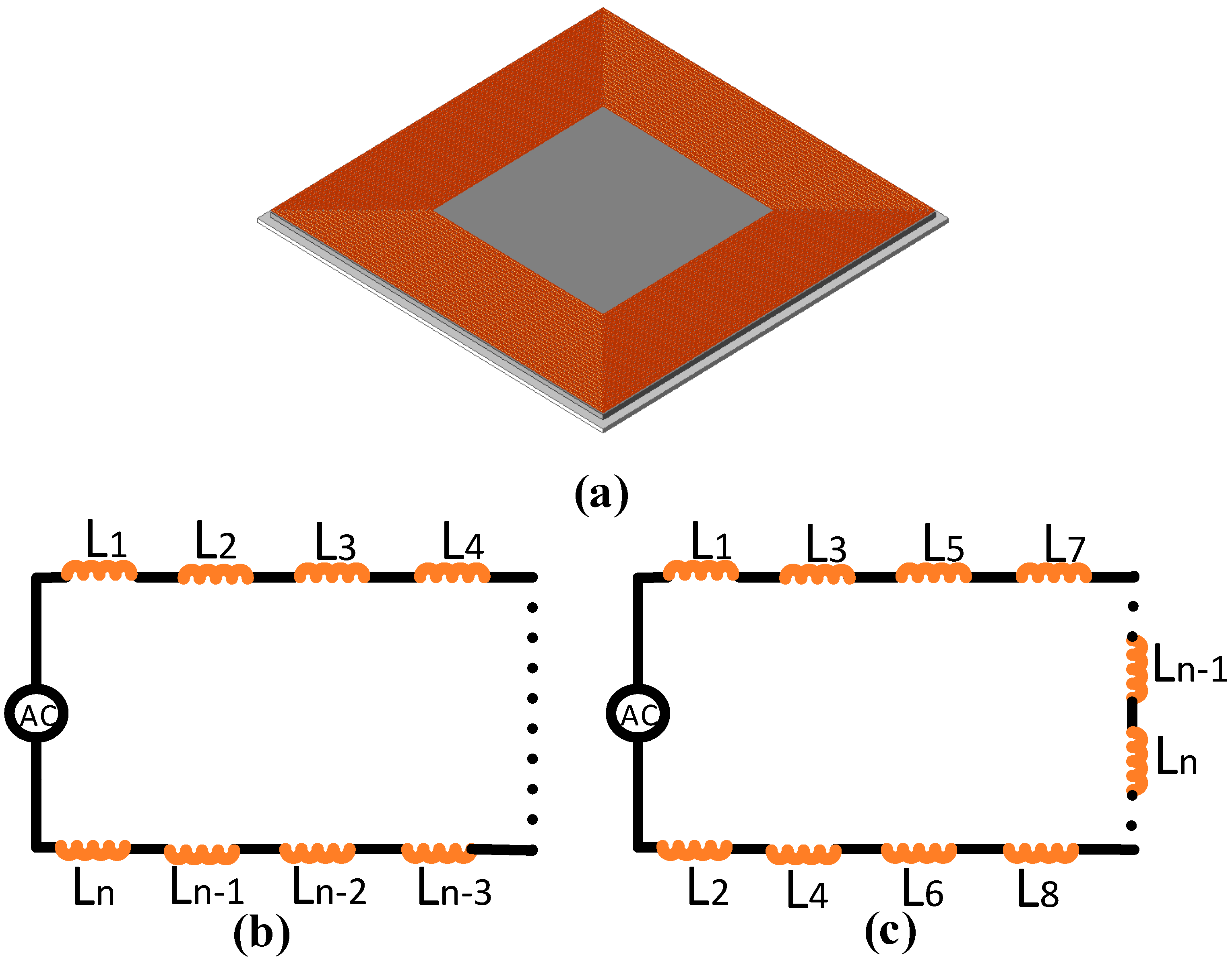
The traditional sequential coil, represented by its equivalent circuit in
Figure 3b, energizes adjacent coil segments uniformly and sequentially, producing in-phase voltage relationships across all turns. This behavior arises from the symmetric winding geometry and strong magnetic coupling between turns, which induce nearly identical time-varying voltages across each turn. Let
Vn denote the voltage across the n-th coil turns. Under in-phase excitation, adjacent voltages satisfy
, where
V0 is the voltage amplitude per turn and
is the angular frequency at the operating frequency
. As a result, the total voltage across the coil accumulates linearly:
Here,
Vtotal represents the cumulative voltage from the coil’s input to output terminals. This additive voltage behavior amplifies the voltage gradient across the coil and directly contributes to elevated electric field emissions. Such a field buildup exacerbates electromagnetic interference and complicates compliance with EMC regulations. In contrast, the AVPC configuration, physically implemented as shown in
Figure 2c and abstracted in the SPICE equivalent circuit of
Figure 3c, strategically alternates voltage phases across adjacent segments. The induced voltage in each turn is governed by:
where
is the self-inductance of the
i-th turn,
the current, and
is the mutual inductance between turns
i and
k. The negative sign in the mutual term (
) is not identical, arising from the opposing flux linkage due to interleaved winding geometry, inherently enforcing a 180° phase inversion mechanism that distinguishes AVPC from traditional topologies. Consequently, adjacent voltages in AVCP satisfy:
This explicit 180° phase relationship ensures destructive interference in the spatial electric field. Mathematically, the phasor sum for adjacent turns cancels:
This expression indicates that the phasor sum of adjacent turn voltages cancels mathematically due to their phase opposition. However, this cancellation does not imply a zero electric field in space. Instead, it reflects a reduction in the local voltage gradient, the principal driver of E-field intensity. In practice, spatial separation, parasitic capacitance, and non-ideal coupling prevent perfect cancellation. As a result, the electric field is not eliminated but significantly attenuated, as confirmed by both FEM simulations and experimental measurements. This destructive voltage interference enabled by the interleaved coil structure and mutual inductive coupling reduces net spatial E-field emissions when the phase-inversion pattern is preserved, as confirmed by detailed SPICE waveform simulations. SPICE simulations further isolate local voltage deviations using the normalized voltage, defined as:
This formulation subtracts the average voltage across all turns, eliminating the common-mode component and highlighting inter-turn voltage differentials. In traditional windings, reflects uniform voltage distribution, whereas in AVPC coils confirms the dominant 180° phase opposition introduced by the sequential inversion strategy. SPICE simulations further validate this behavior, emphasizing AVPC’s role in E-field mitigation.
3.1. Capacitor Placement Impact on Coil Performance
Using the coil dimensions and design parameters from
Table 1, ANSYS FEM simulations were conducted to extract the self-inductances and inter-turn coupling coefficients. These extracted electromagnetic parameters were then used to construct equivalent multi-inductor SPICE models. By inserting tuning capacitors at different turn positions in these circuit models, we simulated the coil’s node voltages and phase relationships under various segmentation schemes. This modelling approach ensures that the waveform results reflect the coil’s physical electromagnetic behavior, linking capacitor placement directly to the observed voltage distribution and E-field emission in the system. Theoutcomes of this analysis, illustrating how the choice of capacitor locations influences waveform symmetry and, in turn, the coil’s radiated electric field.
Figure 4 illustrates example capacitor placements for both coil topologies. In
Figure 4a, capacitors are placed at turns 1, 5, 10, and 15 of a traditional winding coil, representing a typical segmentation strategy used to smooth voltage distribution. In
Figure 4b, capacitor placement is shown for the sequential inversion winding coil configuration, with capacitors located at turns 1, 6, 12, and 18. Although only one configuration is shown for each topology, both capacitor arrangements (1, 5, 10, and 15 and 1, 6, 12, and 18) were applied to both the traditional and AVPC coils during simulation and experimental testing. These diagrams serve to visually convey the segmentation approach implemented in the SPICE, FEM, and experimental analyses, supporting the waveform analyses presented in
Figure 5,
Figure 6,
Figure 7 and
Figure 8. This representation simplifies the visual comparison by displaying only one illustrative example per topology, while the full results are based on all tested combinations. This figure addresses the physical configuration aspect of the simulation models and clarifies the placement strategy referenced in the subsequent waveform analysis.
3.2. Traditional Coil Distributed Capacitor Configuration
To study the impact of distributed compensation on the traditional coil topology, capacitors were positioned at specific coil turns, particularly at segments (1, 5, 10, and 15), and alternatively at (1, 6, 12, and 18), within a 22-turn winding (
Figure A1). These positions were chosen to assess whether varying capacitor placements influence local voltage waveform characteristics or inter-turn relationships. SPICE simulations (
Figure 5a,b) clearly illustrate that, regardless of capacitor placement strategy, adjacent coil turns voltages remain constructively additive, as indicated by the consistent direction of voltage differences shown by the arrows. Although traditional coil winding typically results in voltages between adjacent turns being predominantly in-phase and constructively additive, minor localized phase inversions are occasionally observed (e.g., between turns V
5–V
6, V
11–V
12, and V
17–V
18 in
Figure 5a, and turns V
9–V
10 and V
17–V
18 in
Figure 5b). These isolated inversions can be attributed to local impedance discontinuities introduced by discrete capacitor placements and segmentation effects. Importantly, such localized phenomena are limited in scope and do not indicate systematic destructive interference. Therefore, the overall voltage distribution and E-field emissions in traditional coils remain largely driven by constructive addition, with minor local deviations due to practical capacitor placements.
Specifically, the simulation results show that the voltage difference arrows between adjacent coil turns maintain the same polarity across the coil length, indicating constructive addition rather than cancellation of voltages. Consequently, this confirms that the moderate reductions in E-field intensity observed in traditional coils result solely from voltage gradient smoothing rather than from destructive interference. Importantly, comparing the two capacitor placement scenarios depicted in
Figure 5a,b reveals negligible differences in their voltage distribution characteristics. Thus, the simulation conclusively demonstrates that capacitor placement has minimal impact on inter-turn phase relationships in sequential winding structures, and E-field mitigation arises predominantly from local smoothing of voltage distributions.
Figure 5.
Traditional winding coil of 22 turns with capacitor placement in each turn. (a) Capacitor placed at turns of winding (1, 5, 10, and 15). (b) Capacitor placed at turns of winding (1, 6, 12, and 18).
Figure 5.
Traditional winding coil of 22 turns with capacitor placement in each turn. (a) Capacitor placed at turns of winding (1, 5, 10, and 15). (b) Capacitor placed at turns of winding (1, 6, 12, and 18).
3.3. Capacitor Placement in the SIW Coil
Figure 6b shows the simulated voltage waveforms for each coil segment when the capacitors are placed at segments 1, 6, 12, and 18, representing an example of improper segmentation in the SIW configuration. These waveforms reveal clear deviations from the ideal behavior. Notably, the voltage peak magnitudes are non-uniform across the coil, with some segments reaching higher voltages than others, indicating an unbalanced voltage distribution. The waveforms also lack symmetry; the positive and negative peaks for a given segment are not equal in magnitude, suggesting that the oscillations are not centered around zero as cleanly as in the optimal design.
In the ideal SIW coil with proper capacitor placement (
Figure 6a), adjacent segments largely exhibit consistent near-180° anti-phase relationships. However, localized in-phase behavior, such as that observed between turns V
13–V
14 and V
21–V
22 was noticed even under proper segmentation. These deviations may be attributed to the inherent complexity of phase behavior in segmented coils, where even slight shifts in segment impedance or coupling interactions within the circuit model can produce localized phase mismatches. While the overall SIW structure enforces near-consistent 180° opposition across the majority of turns, such localized deviations are consistent with the sensitivity of the winding to segmentation precision. Therefore, while these minor mismatches may reduce the ideal cancellation slightly, they do not negate the effectiveness of the SIW strategy in suppressing E-field emissions. Future work will focus on refined segmentation tuning or enhanced modeling of distributed parasitics to further improve uniformity.
Figure 6.
Coil voltage waveforms of sequential inversion winding coil. (a) Capacitor placed at turns (1, 5, 10, and 15). (b) Capacitor placed at turns (1, 6, 12, and 18).
Figure 6.
Coil voltage waveforms of sequential inversion winding coil. (a) Capacitor placed at turns (1, 5, 10, and 15). (b) Capacitor placed at turns (1, 6, 12, and 18).
In contrast, improper capacitor placement (
Figure 6b) shows that the phase shift between most adjacent coil segments deviates significantly from the ideal 180° opposition. This widespread phase misalignment clearly indicates improper segmentation. As seen, most segment pairs no longer achieve the expected anti-phase voltage pattern. The loss of systematic phase inversion is evident in both waveform asymmetry and spatial E-field distribution, as shown in the
Section 4.2. Such substantial deviations from ideal behavior compromise the intended destructive interference mechanism, thereby significantly increasing E-field emissions. Consequently, with improper segmentation, the coil segments are no longer in strict phase opposition, resulting in a net time-varying electric potential along the coil, producing additional displacement current (∂D/∂t). This increased displacement current directly elevates electric field emissions, particularly in near-field regions above the coil surface, highlighting the critical sensitivity of SIW coil performance to precise capacitor placement.
5. Experimental Setup
To experimentally validate the E-field mitigation performance of distributed compensation, physical prototypes of traditional and Sequential Inversion Winding coils were constructed as detailed in
Table 1. The SIW coil enforced a 180°voltage phase shift through interleaved turns, while the traditional coil employed a sequential winding configuration. As part of the coil platform construction, an aluminum shielding plate (2 mm thickness) was installed directly beneath the coil to suppress downward E-field leakage and emulate realistic grounding effects. A ferrite core (material: PC40, dimensions: 460 mm × 460 mm × 2.5 mm) was positioned between the coil and shielding plate to enhance magnetic coupling and direct flux upward. This stacked configuration replicates a typical IPT transmitter pad used in EV charging systems as depicted in
Figure 10. The two capacitor placement schemes previously analyzed in
Section 4 were implemented for both coil types.
The measurement setup (
Figure 10) utilized an LCC compensation network operating at 85 kHz, with passive elements (LP and Cp1-Cp4) configured and E-field measurements were obtained using an NF-5035 near-field electric field probe positioned 50mm above the coil surface. Spatial measurements were taken at four coordinates, (X, Y) = (0, ±150 mm), (±150 mm, 0). While exact sensor placement was subject to minor positioning deviations due to practical constraints, it corresponded to the FEM-predicted E-field (
Section 4.3). Each configuration was tested over three independent trials to account for environmental variability, including ambient EMI and conductive surroundings. E-field values were averaged, with standard deviation occasionally exceeding ±10%, reflecting real-world influences on measurement fidelity. Prior to assembly, individual capacitor values were measured and confirmed to lie within a ±3% tolerance range. System resonance at 85 kHz was verified after placement, confirming proper compensation despite small component-level variations.
Figure 11 shows the spatial E-field readings for each coil design. The tests were conducted under realistic lab conditions to capture environmental variability. Variations in measured E-field values were observed, influenced by nearby metallic objects and ambient electromagnetic interference factors relevant to real-world EV charging scenarios and the public EMF exposure limit of 87 V/m at 85 kHz (per EU Directive) [
9]. Among all configurations, the SIW coil with capacitors placed at turns 1, 5, 10, and 15 showed the lowest variability in E-field intensity, suggesting enhanced resilience to environmental disturbances and better electromagnetic stability in uncontrolled settings.
5.1. Experimental Correlation with Simulation Results
The electric field simulation results presented in
Figure 9 were validated through detailed experimental measurements, as summarized in
Figure 12. These experimental data illustrate measured E-field intensities across various spatial points for each coil configuration, allowing direct comparison with the corresponding FEM-predicted distributions. The SIW coils, particularly with capacitors placed at turns 1, 5, 10, and 15, consistently exhibited significantly lower E-field levels compared to traditional coil configurations. Specifically, the SIW coil with optimal capacitor placement maintained measured E-field strengths below 200 V/m across all test points. Conversely, the misaligned SIW coil configuration (turns 1, 6, 12, and 18) resulted in substantially higher measured fields, surpassing 1000 V/m at some spatial positions, consistent with simulation predictions. Traditional coil configurations displayed intermediate E-field strengths, with minimal dependence on capacitor placement. It is important to emphasize that the E-field measurements presented here were taken at a vertical height of 50 mm above the coil surface, representing a deliberately selected worst-case proximity for near-field characterization. These values reflect localized pointwise magnitudes and are not intended for direct comparison with ICNIRP biological exposure limits. Specifically, ICNIRP (2010) recommends internal electric field averaging over 2 × 2 × 2 mm
3 tissue volumes to assess electrostimulation thresholds [
9]. For external fields, spatial averaging procedures are left to the relevant standardization bodies. For formal compliance, standards like IEEE C95.1 [
10] require specific averaging protocols beyond our scope. As such, our pointwise values likely represent a conservative overestimate of actual exposure.
Moreover, in practical EV charging scenarios, physical shielding and typical user distances (>0.5 m) significantly reduce exposure levels. For example, Cirimele et al. [
26] showed that ICNIRP magnetic field limits may be exceeded only at distances below 75 cm from rear-mounted IPT systems. Similarly, Zhao et al. [
27] confirmed compliance for various power levels up to 150 kW when user separation exceeds 0.5–1.7 m. While our measurements focus on electric fields, both studies affirm that worst-case peaks decline rapidly with distance. Furthermore, the observed steep lateral E-field gradients (e.g., 148–1100 V/m variation in
Figure 12) are characteristic of resonant near-field WPT operation and align with spatial behavior reported in prior magnetic field studies [
26,
28]. These gradients are critical when identifying local maxima for emission control. Although not varied experimentally, the E-field magnitude is expected to scale approximately as E ∝ √P with respect to power, consistent with resonant system behavior [
29]. This relationship supports the broader scalability of our findings to higher-power applications.
These measurement results closely correlate with FEM simulations, reinforcing the validity and accuracy of the numerical models employed. Although slight variations between experimental and simulation results occurred due to practical environmental influences such as nearby metallic structures and ambient electromagnetic interference, these measurements nonetheless support the effectiveness of phase-synchronized distributed compensation. Although the measured E-field levels for the optimal SIW configuration remain well below the IEC 61980-3 defined worst-case exposure thresholds [
9], underscoring the practical viability and EMC compliance benefits of employing precisely aligned capacitor placements within SIW-based wireless power transfer systems.
It is also worth addressing the small deviations observed across spatial measurement points in
Figure 12, which ideally should be symmetric. While the coil geometries are symmetric in design, perfect experimental symmetry is difficult to maintain due to slight probe misalignments (±5 mm), environmental factors (e.g., nearby reflective surfaces, metallic structures), and manufacturing tolerances in winding and capacitor positioning. Notably, the AVPC (1-5-10-15) configuration showed the most uniform profile among all cases, indicating not only its E-field reduction capability but also enhanced spatial consistency. This consistency further strengthens its suitability for minimizing emissions in real-world applications. While suppression of E-field components may affect the local wave impedance, FEM simulations confirm that the H-field remains well-confined by the ferrite structure and does not exceed typical safety thresholds. This demonstrates that the AVPC topology offers dual benefits, effective reduction of capacitive emissions while maintaining stable magnetic field behavior within safe limits. It should also be noted that while this study focuses on electric field emission behavior, additional evaluation would be necessary in safety-critical environments, especially for users with implantable medical devices. Interference with such devices may occur at field levels below general ICNIRP thresholds, particularly in the low-frequency range around 85 kHz. Although not directly evaluated here, this is an important consideration for real-world deployment. Notably, the AVPC configuration (capacitors at turns 1, 5, 10, and 15) consistently maintained E-field levels below 220 V/m at all measurement points, reducing the potential for EMI with implantable medical devices even under close-range, unshielded conditions. While our work does not simulate specific implantable device models, these findings provide valuable preliminary guidance for emission-aware design, particularly in ensuring spatial E-field suppression near the coil surface.
5.2. Error Analysis and E-Field Contribution by Coil Type
To complement
Figure 13, it is important to emphasize that accurate E-field measurements in a laboratory environment are inherently subject to variations due to uncontrollable environmental factors. These include surrounding conductive materials, ambient EMI sources, and slight probe positioning discrepancies. In our setup, the NF-5035 probe was mounted on a non-conductive arm to eliminate hand/body interference, and the sensor height was referenced to the approximate center of the internal E-field sensing element, located just beneath the front screen of the probe body (not the outer casing), to improve spatial accuracy. As a result, pointwise agreement between experimental and simulated E-field values may not be exact. Although a separate calibration in a uniform reference field was not performed, the use of consistent positioning and repeatable environmental conditions across all coil configurations supports the relative accuracy of the data.
Despite these limitations, the overall emission profile remains a reliable performance indicator. Across all tested positions, the SIW coil with capacitor segmentation at (1, 5, 10, and 15) consistently exhibited in
Figure 13a, the lowest E-field magnitudes in both simulation and experimental domains. This trend reaffirms the coil’s superior electromagnetic behavior, demonstrating not only effective E-field suppression but also robustness to real-world disturbances. By comparison, traditional coils and improper compensation schemes showed higher emission levels and greater susceptibility to measurement variability.
Figure 13b presents the distribution of average experimental E-field contributions by configuration. The SIW (1,5,10,15) configuration accounted for only 7.9% of the total E-field exposure, confirming its superior suppression capability. Conversely, the SIW (1,6,12,18) case contributed over half (51%) of the total E-field, reinforcing the critical importance of phase-aligned capacitor placement and correlating with disrupted cancellation in FEM results (
Figure 8c,d). These results collectively validate the SIW coil’s effectiveness in suppressing radiated emissions through phase-coherent compensation, establishing capacitor placement as a primary design constraint in phase-inverted topologies, a fundamental shift from its role as a secondary tuning parameter in traditional coils. These findings also reinforce the importance of localized peak suppression in near-field IPT systems, where steep spatial gradients can lead to concentrated emission zones.
As shown in
Section 5.1, the electric field magnitude can vary by nearly an order of magnitude across a small area, highlighting the practical significance of topology-based mitigation. While this study was conducted at a fixed power level (5 A input current), the general relationship E ∝ √P, well established in resonant WPT systems [
29], suggests that electric field magnitudes will scale with increasing power. This implies that the spatial emission patterns observed here may intensify under higher-power operation unless actively mitigated through coil design and phase-controlled compensation.
6. Limitations of the Study
Although comprehensive FEM simulations and experimental validations were conducted, certain limitations should be considered. FEM models inherently involve simplified assumptions, including idealized material properties, boundary conditions, and meshing approximations, potentially leading to minor deviations from practical coil performance. Experimental validation, while rigorous, was performed in normal laboratory conditions, where slight inaccuracies in probe positioning and the presence of ambient electromagnetic interference or reflections could introduce measurement variability.
Additionally, actual operational environments for wireless EV charging might significantly differ from the experimental setup due to varying ambient temperatures, humidity, and infrastructure interactions. Coil manufacturing tolerances, specifically slight deviations in winding precision and capacitor placements, may also affect the phase alignment and thus compromise the optimal performance of the Sequential Inversion Winding coil configuration. Further practical studies, incorporating broader environmental and operational conditions, are recommended to comprehensively address these limitations.


