Abstract
The field emission current in a vacuum (, where and are constants) depends on the electric field strength E. In other words, the differential resistance in a vacuum does not follow Ohm’s law. Therefore, the relationship governing the capacitance and current between two electrodes in a vacuum is an intriguing research topic. In this study, we constructed an interface structure in which contact areas and non-contact vacuum areas coexisted by adhering two Si wafers and measuring the capacitance characteristics of this structure. A volatile capacitance appeared at the interface, with the contact areas contributing to positive capacitance and the vacuum areas contributing to negative capacitance. The tunneling current passing through the interface played an important role in the formation of the negative capacitance.
1. Introduction
Recently, research concerning negative capacitance has attracted considerable interest [1,2,3,4,5,6]. In these studies, the negative capacitance is related to the physical properties of the dielectric material between the electrodes. This type of negative capacitance has been observed in only a limited number of materials, such as Zr0.5Hf0.5O2, and typically exhibits a low capacitance value. Moreover, integrating this phenomenon into silicon-based materials commonly used in electronic devices remains a significant challenge [1,7,8]. Unlike the negative capacitance due to material properties, our research group proposed a two-resistor structure model and generated negative capacitance by controlling the tunneling current across the interface of the two-resistor structure [9]. Ohm’s law does not apply to the tunneling current, which behaves as a field emission current in relation to the potential difference across the two resistors. In other words, the differential conductance is not constant. As a result, the amount of free charge accumulated on the electrodes varies with changes in current and voltage, indicating that this two-resistor structure exhibits volatile capacitance. When the charge decreases with increasing voltage, the volatile capacitance becomes negative. Conversely, when the charge increases, the capacitance becomes positive. Since these are free charges, they dissipate through conductive pathways once the circuit power is turned off, causing the capacitance to vanish [9].
The equivalent circuit of a resistor with two parallel-plate electrodes consists of the parallel circuit of and the capacitor . The capacitance varies depending on the value of resistance . If is infinite, the capacitance is determined by the dielectric constant of the insulator . Moreover, when depends on the potential difference across the resistor—that is, when —the relationship between the electrode charge and does not follow Ohm’s proportional relationship. As leaks through the resistor , the capacitance becomes volatile. Our theoretical study revealed that the volatile capacitance is determined by the correlation between the differential current and the Ohmic current . The conclusions are that when , ; when , ; and when , [9]. Furthermore, our experiments confirmed the transition between positive and negative capacitance in the interface structure of a multi-walled carbon nanotube resistor and vacuum, and the results obtained were consistent with theoretical predictions [9].
In this study, we investigated the volatile capacitance characteristics of a two-resistor structure constructed using Si crystals. Valuable results were obtained regarding the role of the tunneling current in the capacitance characteristics.
2. Experimental
The p-type Si (100) wafers of thickness 520 μm and resistivity 10 Ω·cm have undulations on one side. Figure 1a,b show an SEM image of the surface and a cross-sectional schematic diagram of the undulating Si wafer, respectively. Figure 1c shows the pattern of the contact area between the undulating wafers, and Figure 1d shows the pattern of the contact area between the undulating wafer and the untreated wafer. As shown in Figure 1a,b, the cross section was an equilateral triangle with a 4 μm distance between vertices. An aluminum thin film of thickness 100 nm was fabricated on one side of the Si wafer to form Ohmic contact, as shown in Figure 1b. The undulating surfaces of the two wafers faced each other, set at 90° in the γ direction, to form sample A with point contact, as shown in Figure 1c. The contact points were assumed to be circular with a diameter of . Additionally, sample B with line contact, as shown in Figure 1d, was formed by facing an undulating and a non-undulating wafer. The contact line width was assumed to be . Samples A and B were square with a side length of 3 mm. A conceptual diagram of the two-resistor structure is shown in Figure 2. The average distance between the two resistors is denoted by . The surface roughness of the silicon wafers was evaluated using a 3D scanning electron microscope (ELIONIX Inc. ERA-8800, Tokyo, Japan), revealing an average roughness of 0.20 μm. It was confirmed that the undulation treatment significantly increased the roughness of the wafers. The current passing through the interface is the sum of the conduction current and the polarization current through the contact areas and the tunneling current through the non-contact vacuum areas. This interface, composed of contact and non-contact areas, formed the core of the negative capacitor structure. Based on the average separation distance and the potential difference between the two resistors, the interfacial electric field strength was determined to exceed 6.25 V/μm. The field emission threshold of p-type Si micro-tip arrays is 4.0–5.0 V/μm [10,11]. Therefore, it is feasible to generate a tunneling current passing through the interface of a two-Si wafer structure.
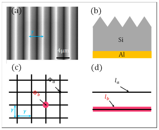
Figure 1.
Surface SEM image (a) and cross-sectional schematic diagram of the undulating Si wafer (b), the pattern of contact area between the undulating wafers (c), and the pattern of contact area between the undulating wafer and the untreated wafer (d).
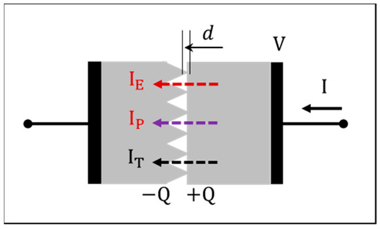
Figure 2.
Conceptual diagram of the two-resistor structure.
Samples A and B were placed in a vacuum chamber with a base vacuum of , and their electrical characteristics were measured with an impedance analyzer (HIOKI, IM3570, Nagano, Japan) while varying the distance , DC bias, and AC amplitude. To overcome the difficulty of controlling the distance , it was adjusted using screws. The screw was rotated approximately 2° to change the distance . Due to the presence of contact areas between the wafers caused solely by gravity, accurately measuring the average separation distance d was challenging. Additionally, tightening the screws altered the roughness of the surface, making it difficult to reproduce consistent measurement values. Therefore, we chose to keep the screws tightened throughout the experiment without loosening them. In addition, a constant-current source was employed during the measurements in this study.
3. Results and Discussion
The frequency dependence of the capacitance for samples A and B at various is shown in Figure 3a,b, respectively. The color bar in the figure represents the number of measurements taken. For sample A, in the frequency range below , the capacitance changed from negative to positive and then back to negative with decreasing , in the order of . In the frequency range above , the capacitance remained almost constant at at 1 MHz.
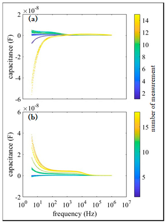
Figure 3.
Frequency dependence of capacitance for samples A (a) and B (b) at various values. The color bar in the figure indicates the number of measurements.
For sample B, negative capacitance appeared in the frequency range below , increasing to positive with decreasing , up to the order of . Above , the capacitance remained almost constant at at 1 MHz. These results suggest that the process of the two resistors approaching one another could be divided into two stages. In the first stage, with zero contact area between the two resistors, a tunneling current can occur if the resistors become sufficiently close. The initial negative capacitance with decreasing can be attributed to the tunneling current. In the second stage, contact occurs between the two resistors, generating conduction and polarization currents in addition to the tunneling current, forming a positive capacitance component. A further reduction in the distance between the two resistors changes the contact area and the proportion of tunneling current. As shown in Figure 1, the contact area patterns of samples A and B are point and line, respectively. Assuming the diameter of the tunneling current point and the width of the tunneling current line to be and , respectively, the area ratio of the tunneling current can be estimated. For sample A, the ratio is . For sample B, the ratio is . Assuming that and , we obtain , where . In consideration of the resistance of the conduction and polarization currents, the proportion of tunneling current in sample A was greater than that in sample B. Thus, the smaller negative capacitance in sample B can be attributed to a smaller proportion of tunneling current. Assuming decreases and and increase , the condition holds in sample B with the larger contact area, resulting in positive capacitance. This explains the results observed in Figure 3.
The frequency dependence of the capacitance for samples A and B at various DC biases is shown in Figure 4a,b, respectively. Here, the AC amplitude is 2.5 V, is set to its minimum value, and the color bar indicates the DC bias. The DC bias dependence of negative capacitance was strong in sample A, which had a large proportion of tunneling current. In contrast, in sample B, where the conduction and polarization currents were dominant, there was almost no DC bias dependence of capacitance. It is understood that the DC bias does not affect the differential current of the conduction and polarization currents , but does affect the differential resistance corresponding to the tunneling current.
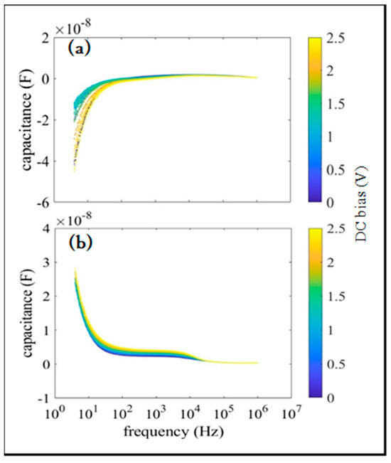
Figure 4.
Frequency dependence of capacitance for samples A (a) and B (b) at various DC biases. Here, the AC amplitude is 2.5 V, is set to its minimum value, and the color bar indicates the DC bias.
The frequency dependence of the capacitance for samples A and B at various AC amplitudes is shown in Figure 5a,b, respectively. Here, the DC bias is 2.5 V, is set to its minimum value, and the color bar indicates the AC amplitude. It was confirmed that the AC signal was periodic and did not affect the charge . This resembles the behavior typically observed in dielectric capacitors [12,13].
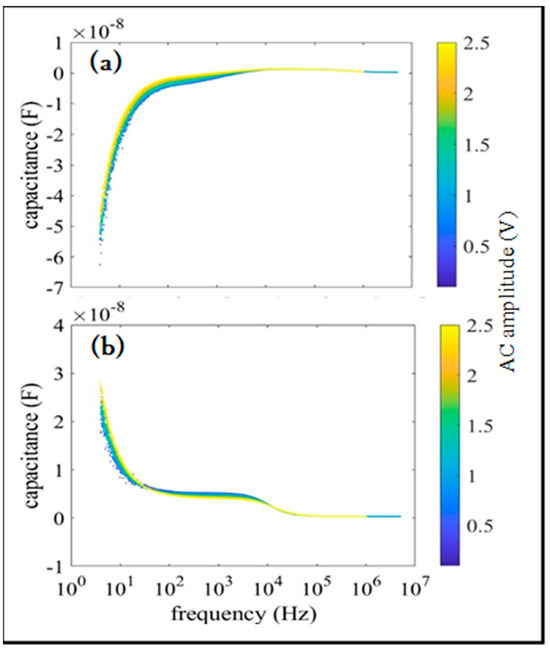
Figure 5.
Frequency dependence of capacitance for samples A (a) and B (b) at various AC amplitudes. Here, the DC bias is 2.5 V, is set to its minimum value, and the color bar indicates the AC amplitude.
The results indicate that negative capacitance, i.e., inductance without a coil, may be achieved. Furthermore, it was confirmed that the phase delay of the current relative to potential is related to the time constant of an RC circuit. The frequency dependence of the time constant for samples A and B at various is shown in Figure 6a,b, respectively. Here, and represent the resistance and capacitance of the series equivalent circuit of the samples. Additionally, the straight lines in the figure indicate the half-periods of the AC signal. As can be observed by comparing Figure 3 and Figure 6, negative capacitance occurred in the low-frequency region where the half-periods of the AC signal were greater than . In other words, the relationship must be established to form a negative capacitance. Under this condition, the tunneling current is sustained along with the AC signal. Conversely, when , the duration of sustained tunneling current during the AC signal is shorter, with periods where it reaches zero. In other words, the sustained tunneling current plays a crucial role in forming negative capacitance. Furthermore, peaks in the time constant can be observed in Figure 6a,b under conditions where negative capacitance was generated. This can be attributed to the resonance between the negative capacitance (inductance) of the two-resistor structure and the positive capacitance of the Al electrodes [14,15].
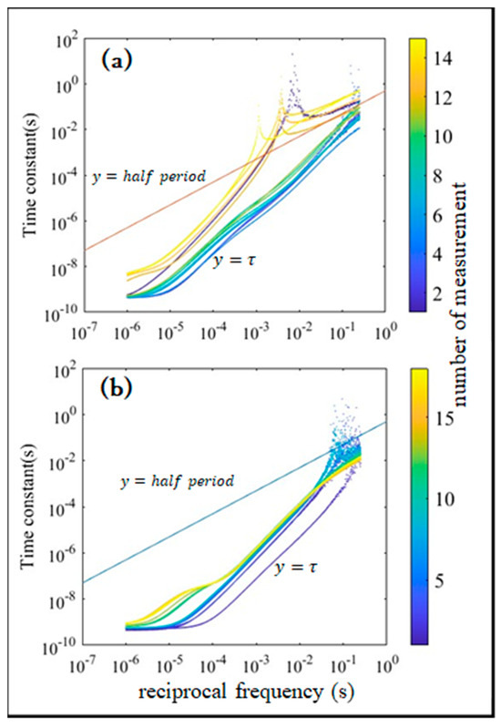
Figure 6.
Frequency dependences of the time constant for samples A (a) and B (b) at various values.
Figure 7a,b present the Cole–Cole plots for samples A and B at various values, respectively, with enlarged insets on the vertical axes. Corresponding to the results of Figure 3 and Figure 6, negative capacitance was observed in both samples A and B in the low-frequency region below . As the frequency increased, the imaginary part of the impedance traced a semicircular path. The absolute value of the negative capacitance decreased with increasing frequency, passing through a minimum value and eventually becoming positive capacitance. As the − approached zero, reached its maximum value, corresponding to the peak of in Figure 6a,b.
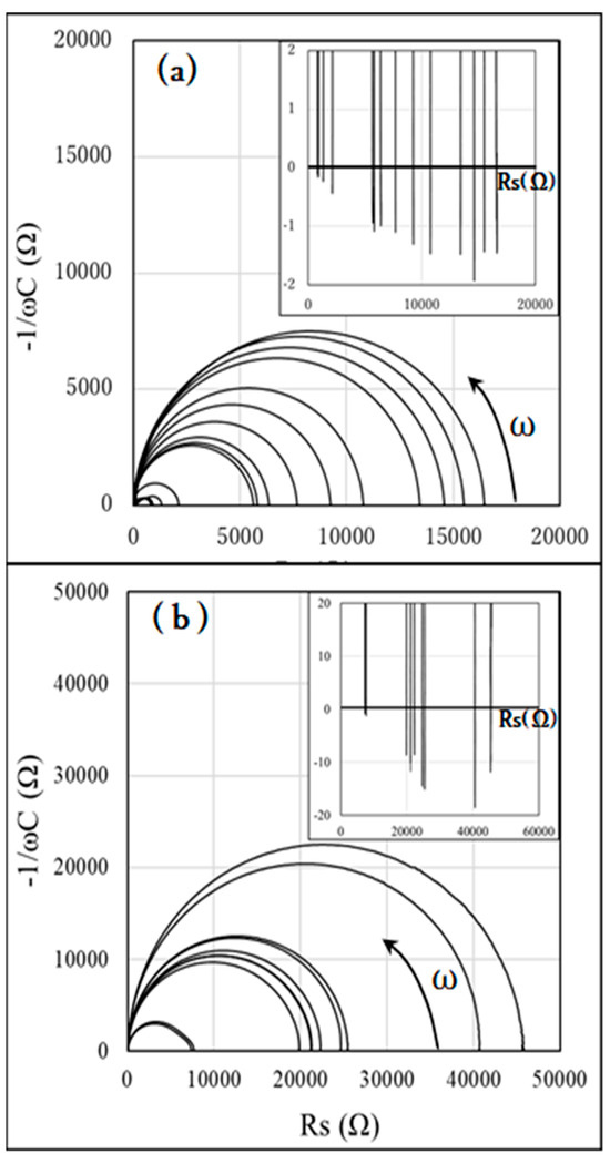
Figure 7.
Cole–Cole plots for samples A (a) and B (b) at various values.
Based on these results, we now examined the characteristics of negative capacitance. Notably, negative capacitance was observed only in the low-frequency region within the two-silicon-resistor structure. At low frequencies, sufficient time was available for the charge to respond to conduction current, polarization current, and tunneling current, which is essential for the emergence of negative capacitance.
Second, negative capacitance was influenced by the applied DC bias yet remained unaffected by variations in the AC signal amplitude. This suggests that the phenomenon is governed primarily by the steady-state electric field rather than dynamic excitation.
Third, by adjusting the spacing between the two resistors, the interface capacitance can be modulated, transitioning between positive and negative values. This tunability highlights the critical role of geometric configuration in controlling interfacial charge dynamics.
Fourth, tunneling current played a pivotal role in the emergence of negative capacitance. By facilitating charge leakage, it enabled the condition , which is fundamental to the manifestation of negative capacitance. This behavior underscores the importance of quantum mechanical effects in modulating interfacial charge dynamics within the two-resistor structure.
Fifth, contact resistance at the interface of the two-resistor structure contributed to the accumulation of charge , thereby enabling the condition , which leads to positive capacitance. This effect highlights the role of resistive interfaces in stabilizing charge buildup and promoting conventional capacitive behavior.
Finally, the capacitance of the two-resistor structure exhibited volatility. Conduction and tunneling currents diminished to zero only when the contact resistance approached infinity. Under this condition, charge accumulation driven solely by the polarization current became observable, marking a transition to a purely capacitive response. This behavior underscores the dynamic interplay between resistive and quantum transport mechanisms in determining the system’s capacitive state.
4. Conclusions
In conclusion, we fabricated an interface structure by applying angulation processing to the surface of a silicon crystal, enabling contact between two resistors. Our findings reveal that contact regions, where conduction and polarization currents dominate, contribute to positive capacitance. In contrast, non-contact regions, characterized by tunneling current flow, give rise to negative capacitance. This dual behavior underscores the spatial dependence of charge transport mechanisms within the structure. Notably, the observed negative capacitance effect holds significant potential for the development of two-dimensional inductor devices and coil-free integrated circuits, offering a promising pathway toward compact and energy-efficient electronic components.
Author Contributions
Conceptualization, H.Y. and Y.S.; methodology, S.K.; software, H.Y.; validation, H.Y., S.F. and S.K.; formal analysis, H.Y., Y.T., S.F., K.Y., S.K. and Y.S.; investigation, H.Y., Y.T., S.F. and K.Y.; resources, Y.S.; data curation, H.Y.; writing—original draft preparation, H.Y.; writing—review and editing, Y.S.; visualization, H.Y. and S.F.; supervision, Y.S.; project administration, Y.S.; funding acquisition, Y.S. All authors have read and agreed to the published version of the manuscript.
Funding
This work was partially funded by the Takahashi Industrial and Economic Research Foundation (grant number: 12-003-101) and the Grant-in-Aid for Scientific Research (C), Japan Society for the Promotion of Science (JSPS) (grant number: 23K03868).
Data Availability Statement
The original contributions presented in this study are included in the article. Further inquiries can be directed to the corresponding author.
Conflicts of Interest
The authors declare no conflict of interest.
Correction Statement
This article has been republished with a minor correction to the Data Availability Statement. This change does not affect the scientific content of the article.
References
- Salahuddin, S.; Datta, S. Use of negative capacitance to provide voltage amplification for low power nanoscale devices. Nano Lett. 2008, 8, 405–410. [Google Scholar] [CrossRef] [PubMed]
- Zhirnov, V.V.; Cavin, R.K. Negative capacitance to the rescue? Nat. Nanotechnol. 2008, 3, 77–78. [Google Scholar] [CrossRef] [PubMed]
- Liu, L.; Lei, L.; Lu, X.; Xia, Y.; Wu, Z.; Huang, F. Direct measurement of negative capacitance in ferroelectric/semiconductor heterostructures. ACS Appl. Mater. Interfaces 2023, 15, 10175–10181. [Google Scholar] [CrossRef] [PubMed]
- Khan, A.I.; Kim, J.K.; Sikder, U.; Das, K.; Rodriguez, T.; Soman, R.; Chowdhury, S.; Salahuddin, S. Negative capacitance overcomes Schottky-gate limits in GaN high-electron-mobility transistors. Science 2025, 389, 508–511. [Google Scholar] [CrossRef] [PubMed]
- Saha, A.K.; Gupta, S.K. Negative capacitance effects in ferroelectric heterostructures: A theoretical perspective. J. Appl. Phys. 2021, 129, 080901. [Google Scholar] [CrossRef]
- Íñiguez, J.; Zubko, P.; Luk’yanchuk, I.; Cano, A. Ferroelectric negative capacitance. Nat. Rev. Mater. 2019, 4, 243–256. [Google Scholar] [CrossRef]
- Müller, J.; Böscke, T.S.; Bräuhaus, D.; Schröder, U.; Böttger, U.; Sundqvist, J.; Kücher, P.; Mikolajick, T.; Frey, L. Ferroelectric Zr0.5Hf0.5O2 thin films for nonvolatile memory applications. Appl. Phys. Lett. 2011, 99, 112901. [Google Scholar] [CrossRef]
- Hoffmann, M.; Slesazeck, S.; Mikolajick, T. Progress and future prospects of negative capacitance electronics: A materials perspective. APL Mater. 2021, 9, 020902. [Google Scholar] [CrossRef]
- Sun, Y.; Yasunaga, H.; Shiraishi, M.; Sakai, H. Volatile capacitance of resistor with differential resistance. Appl. Phys. Lett. 2024, 125, 143501. [Google Scholar] [CrossRef]
- Karabutov, A.V.; Frolov, V.D.; Loubnin, E.N.; Simakin, A.V.; Shafeev, G.A. Low-threshold field electron emission of Si micro-tip arrays produced by laser ablation. Appl. Phys. A 2003, 76, 413–416. [Google Scholar] [CrossRef]
- Zhou, Y.; Zhang, P. Theory of field emission from dielectric coated surfaces. Phys. Rev. Res. 2020, 2, 043439. [Google Scholar] [CrossRef]
- Izyumskaya, N.; Alivov, Y.I.; Cho, S.J.; Morkoç, H.; Lee, H.; Kang, Y.S. Processing, structure, properties, and applications of PZT thin films. Crit. Rev. Solid State Mater. Sci. 2007, 32, 111–202. [Google Scholar] [CrossRef]
- Khaldi, O.; Jomni, F.; Gonon, P.; Valle’e, C. AC and DC bias effect on capacitance–voltage nonlinearities in Au/HfO2/M (M= Pt, TiN, W, and AlCu) MIM capacitors: Effect of the bottom electrode material. J. Mater. Sci. Mater. Electron. 2020, 31, 19036–19043. [Google Scholar] [CrossRef]
- Dorf, R.C.; Svoboda, J.A. Introduction to Electric Circuits, 8th ed.; John Wiley and Sons: Hoboken, NJ, USA, 2010; p. 368. [Google Scholar]
- Zhang, Y.; Xie, Y.; Chen, C.; Guo, X.; Yan, Y.; Yang, L.; Kang, Y. Comprehensive analysis and optimization of parasitic capacitance on conducted EMI and switching losses in hybrid-packaged SiC power modules. IEEE Trans. Power Electron. 2023, 38, 13988–14003. [Google Scholar] [CrossRef]
Disclaimer/Publisher’s Note: The statements, opinions and data contained in all publications are solely those of the individual author(s) and contributor(s) and not of MDPI and/or the editor(s). MDPI and/or the editor(s) disclaim responsibility for any injury to people or property resulting from any ideas, methods, instructions or products referred to in the content. |
© 2025 by the authors. Licensee MDPI, Basel, Switzerland. This article is an open access article distributed under the terms and conditions of the Creative Commons Attribution (CC BY) license (https://creativecommons.org/licenses/by/4.0/).