Abstract
In this study, we developed a facilitated ferroelectric high-k/metal-gate n-type FinFET based on Hf0.5Zr0.5O2. We investigated the impact of the hysteresis effect on device characteristics of various fin-widths and the degradation induced by stress on the ferroelectric FinFET (Fe-FinFET). We clarified the electrical characteristics of the device and conducted related reliability inspections. For the Fe-FinFET, the hysteresis behavior of the Hf0.5Zr0.5O2-based gate stack in the Si-fin body is apparent, especially at narrower fin-widths, which affects device performance and reliability under voltage stress. The gate ferroelectric film is worsened after voltage stress with higher impact ionization, resulting in hysteresis degradation and serious induced device performance degradation. It is suggested that the hysteresis degradation is caused by both a shift in polarization of the gate ferroelectric film and generation of interface traps after high-energy carrier stress, which was confirmed by crystal structure inspection.
1. Introduction
Since the negative capacitance property of Hf0.5Zr0.5O2 (HZO)-based ferroelectric materials was proposed in 2008 [1], ferroelectric field-effect transistors (Fe-FETs) have been extensively researched and come to be considered to be highly viable options for low-power-consumption logic devices with low-operating voltage requirements. The reason Fe-FETs are able to overcome physical limitations is due to the negative capacitance property of the ferroelectric layer, which can display a subthreshold swing (SS) of less than 60 mV/decade through dipole switching and arrangement [2,3,4,5,6]. In comparison to conventional MOSFETs, a lower threshold voltage (VTH) can be achieved for Fe-FETs with an ultrasteep SS, which leads to a reduction in the applied voltage (VDD) for a given gate overdrive voltage (VG − VTH) [7,8,9].
In order to meet performance requirements and address the limitations of planar bulk transistors when scaling down to sizes below 22 nm, the semiconductor industry has developed new technologies such as the fin field-effect transistor (FinFET) [10]. The FinFET is considered the most promising candidate for replacing traditional planar bulk devices beyond the 22 nm technology node, owing to their excellent performance in reducing leakage current and improving short channel behavior [11,12]. The primary difference in geometry between a planar MOSFET and a FinFET is that the FinFET device has a non-planar 3D structure. The Si-bulk fin can be covered on three sides by a high-k/metal gate, while the fin-width can be made very thin to minimize the device’s short channel effect. Tri-gate FinFET devices have been developed using different gate stacks, such as Poly-Si/SiON or high-k/metal gate, on bulk-Si substrate [13,14,15]. However, in order to further improve their performance, alternative materials and designs are being explored. Ferroelectric FinFETs (Fe-FinFETs) are an emerging type of transistor that combines the unique properties of ferroelectric materials with the high performance of FinFETs. Fe-FinFETs have been shown to exhibit improved device performance, such as faster switching speeds and reduced power consumption, compared to conventional FinFETs. Among these, Fe-FinFET is a promising option for upcoming applications due to its unique ferroelectric properties [16,17].
A comprehensive understanding of reliability physics is a crucial requirement for the successful commercialization of this promising technology. Hot carrier injection (HCI), which is a well-known reliability issue in modern MOSFET technology, is of great interest due to its important role in device reliability. HCI occurs when high-energy electrons or holes are injected into the gate oxide of a transistor, which can lead to changes in the device’s electrical characteristics over time. Recent studies have shown that HCI can accelerate the degradation of gate oxide in FinFETs, leading to a further reduction in device performance and reliability [18,19]. It is even more severe in FinFETs due to the higher probability of carrier capture in the tri-gate structure and the higher density of available Si-H bonds at (110) fin sidewalls. Except HCI, positive biasing temperature instability (PBTI) is also another reliability issue for FinFET devices. PBTI-induced high electric field effects can result in gate oxide degradation and alter the threshold voltage and subthreshold swing (SS) of the device. [20]. Both HCI and PBTI will affect the Si/interfacial layer (IL) interface of Fe-FinFET devices. The quality of the interface between Si and IL is a crucial factor that impacts the hysteresis phenomenon and device performance of Fe-FinFETs [21]. However, the effect of hysteresis on the reliability characteristics for Fe-FinFETs remains understudied, and there is little research on the relationship between hysteresis and the reliability of Fe-FinFETs.
In this work, the impact of hysteresis on voltage stress-induced device degradation for n-type Fe-FinFETs was investigated. Our findings suggest that the degradation of Fe-FinFETs due to voltage stress-induced device degradation will be more severe because of the deterioration of the hysteresis of the gate ferroelectric film under hot carrier stress, particularly in devices with narrower fin-widths. The primary cause of hysteresis degradation is attributed to the degradation of the Si/IL interface. Furthermore, we observed that after voltage stress with higher impact ionization, which mainly occurs in narrower Si-fin channels, the gate ferroelectric film undergoes severe carrier ion bombardment, resulting in changes in the crystal structure with high hysteresis.
2. Materials and Methods
N-type tri-gate FinFETs were fabricated on SOI wafer with a film thickness of 20 nm. Si film was etched at first to form the Si-fin for oxidation and etch steps. The silicon film was etched to form thin silicon fins with widths from 20 nm to 400 nm and channel lengths from 20 nm to 40 nm, as shown in Figure 1a. B ions were implanted into the Si-fins to form p-well regions for N-type tri-gate FETs. The gates were formed using a replacement metal gate (RMG) process with gate length scaling down to 20 nm. The gate stack shown in Figure 1b includes a 0.6 nm interfacial layer of SiO2 grown by thermal oxidation, a ferroelectric layer deposited by ALD at 250 °C and 5 nm Hf0.5Zr0.5O2 followed by TaN and TiN stack metal film deposition as the gate electrode. The gate insulator effective oxide thickness (EOT) was 1.0 nm. A nickel self-aligned silicidation approach was implemented to reduce the contact resistance between the metal and silicon, followed by a standard tungsten-plug filling process and copper metallization as an interconnection backend. The real fabricated Fe-FinFET structure has a thin (5 nm) ferroelectric layer formed uniformly around Si-fin with a fin-width of 20~400 nm. The electrical characteristics of devices, hot carrier stress and negative/positive biasing-induced instability were evaluated using an Agilent B-1500A semiconductor analyzer. Stress conditions of VGS = 2.3~2.7 V and VDS = 0~2.7 V were utilized in this work.
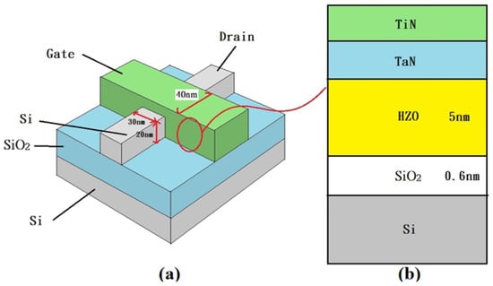
Figure 1.
(a) Schematic diagram of tri-gate ferroelectric FinFET structure, and (b) the related gate stack picture of this fabricated ferroelectric FinFET.
3. Results
Figure 2 shows (a) ID-VG characteristics and (b) transconductance for various fin-widths of n-type Fe-FinFET. Better subthreshold swing but lower drive current could be observed for the narrower fin-width Fe-FinFET. Based on our observations, it was found that decreasing the fin-width of the Fe-FinFETs resulted in an improvement of the subthreshold swing, while simultaneously causing a reduction in the drive current. The obtained result implies that the subthreshold behavior of Fe-FinFETs can be managed by reducing the fin-width. Nevertheless, the reduction in the effective channel width resulted in a corresponding decrease in the drive capability. When the gate voltage sweep is performed from negative to positive, the measured ID-VG curve is referred to as forward (FWD) sweep. Conversely, the sweep from positive to negative is referred to as reverse (RVS) sweep. In this work, the hysteresis value is defined as VTH,RVS-VTH,FWD. A positive hysteresis value indicates that the device exhibits clockwise hysteresis, which is suggested to be caused by electron trapping from the channel. Conversely, a negative hysteresis value indicates counterclockwise hysteresis, which is attributed to the ferroelectric response [22]. Furthermore, it was observed that the devices with narrower fin-width exhibited a larger hysteresis window, indicating a higher density of interface traps.
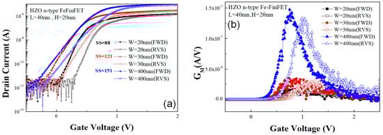
Figure 2.
(a) ID-VG characteristics and (b) transconductance for various fin-widths of n-type Fe-FinFET.
To assess the impact of hot carrier injection-induced stress on Fe-FinFETs, the devices were subjected to a stress condition with VG = VD = 2.3 V for a duration of 5000 s. Figure 3a,b illustrate the ID-VG characteristics and transconductance, respectively, both pre- and post-HCI stress. Following hot carrier stress, the device with a narrower fin-width demonstrated the most severe subthreshold and transconductance degradation. Conversely, we noted that the narrower fin-width Fe-FinFET displayed a more pronounced VTH shift compared to its larger fin-width counterpart, which suggests an increase in the gate ferroelectric hysteresis as the fin-width decreased. It is suggested that a narrower Fe-FinFET results in more significant carrier ion bombardment to the gate ferroelectric film, leading to an increase in the hysteresis effect of the ferroelectric film and ultimately degrading its driving capability. During hot carrier stress, the strongest impact ionization occurs on a narrower fin-width Fe-FinFET, causing interface state generation and resulting in severe SS degradation. In fact, the most significant degradation was observed in 20 nm fin-width devices. Furthermore, this stress-induced device degradation is worsened in narrow fin-width Fe-FinFET due to the more serious gate ferroelectric hysteresis.
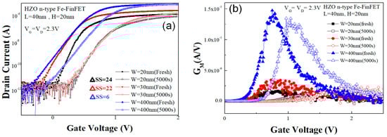
Figure 3.
Hot-carrier-induced (a) ID-VG characteristics and (b) transconductance degradations for various fin-widths of n−type Fe-FinFET.
The impact of hot carrier stress on the subthreshold swing and hysteresis of n-type Fe-FinFETs with varying fin-widths was investigated, as depicted in Figure 4. As shown in Figure 4a, the results revealed that as the fin-width decreased, the SS degraded more severely. Specifically, the degradation rates of SS after 5000 s of hot carrier stress for devices with fin-widths of 20 nm, 30 nm and 400 nm were 27%, 18% and 3%, respectively. Interestingly, this device degradation was found to be correlated with the hysteresis behavior of the gate ferroelectric material, as illustrated in Figure 4b. It could be found that higher hysteresis happened in a narrower fin-width device. The most severe hysteresis degradation of 40% happened on a 20 nm fin-width n-type Fe-FinFET after hot carrier stress for 5000 s, in comparison with 30% and 20% hysteresis degradation, which happened on 30 nm and 400 nm, respectively. Serious hysteresis degradation was caused by impact ionization during hot carrier stress, meaning the device’s gate stack control was also decayed, further resulting in serious device degradation.
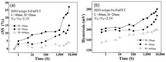
Figure 4.
Hot-carrier-induced (a) subthreshold swing and (b) hysteresis degradations for various fin-widths of n-type Fe-FinFET.
In order to investigate the dependence of the device’s instability on the hysteresis of the gate ferroelectric film, various voltage stress conditions of VD = 0, 2.5 and 2.7 V while VG = 2.7 V were applied to Fe-FinFETs. Devices with fin-widths of 30 nm were utilized in this work. Subthreshold swing degradation for n-type Fe-FinFET under various stress conditions is shown in Figure 5a. It can be observed that the SS degradation increases with the increase in VD, and it is not obvious when VD = 0 V. Figure 5b shows the spread of experimental data for SS degradation versus hysteresis deviation. It could be found that most SS degradation was related to stress-induced hysteresis deviation of the gate ferroelectric. At a stress level where both the VD and VG were set to 2.7 V, a more significant degradation in the SS could be observed. Additionally, there was a greater deviation in hysteresis under this stress condition. During the application of positive bias temperature instability (PBTI) stress, where VD was set to 0 V, there were minimal variations observed in both SS and hysteresis. This was because hot carrier stress caused higher impact ionization, leading to increased interface defects and deterioration of the gate ferroelectric film’s hysteresis. Based on the content provided, it appears that there is a correlation between SS degradation and hysteresis deviation, but the relationship is not entirely positive. This suggests that as SS degradation increases, hysteresis deviation may not always increase in a linear fashion. This implies that hysteresis deviation is not solely caused by interface traps and that another mechanism, which is important to identify, may also contribute to this phenomenon.
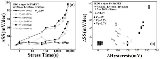
Figure 5.
Subthreshold swing degradation (a) versus stress time and (b) versus hysteresis deviation after various voltage stresses for n-type Fe-FinFET.
In order to investigate the correlation between the gate ferroelectric film and the performance of Fe-FinFET, cross-sectional high-resolution transmission electron microscopy (HRTEM) was performed before and after hot carrier stress, as shown in Figure 6. Prior to hot carrier stress, the HZO-based ferroelectric film exhibited a pure polycrystalline structure (Figure 6a). However, after hot carrier stress, it was observed that the ferroelectric film underwent a transformation to a partially amorphous crystal structure (Figure 6b). Moreover, the Si/IL interface on Fe-FinFET changed from an apparent amorphous/single-crystal Si/IL interface (Figure 6a) to a blurry amorphous/single-crystal Si/IL interface after hot carrier stress (Figure 6b). This change in the Si/IL interface state was found to correspond to device degradation. Furthermore, it is possible that the hysteresis of the gate ferroelectric film may worsen due to the change in the crystal structure of the ferroelectric film after hot carrier stress.
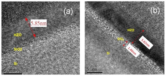
Figure 6.
HRTEM of gate stack for Fe-FinFET (a) before and (b) after hot carrier stress.
In Figure 7, the selected area electron diffraction (SAED) pattern of a gate ferroelectric film for Fe-FinFET is shown before and after hot carrier stress. The SAED image reveals that voltage stress with electrical charging can decay the hysteresis of this ferroelectric FinFET, leading to a change in the crystal properties of the gate ferroelectric film. The main cause of hysteresis degradation is the shift of polarization [23] in the gate ferroelectric film after high-energy carrier stress. This shift in polarization induces a change in the crystal structure of the ferroelectric film from an orthonormal structure with lower hysteresis to an orthogonal structure with higher hysteresis. When subjected to voltage stress, especially in the Si-fin channel where higher impact ionization occurs, the gate ferroelectric film undergoes serious carrier ion bombardment, resulting in further changes to the crystal structure and causing high hysteresis.
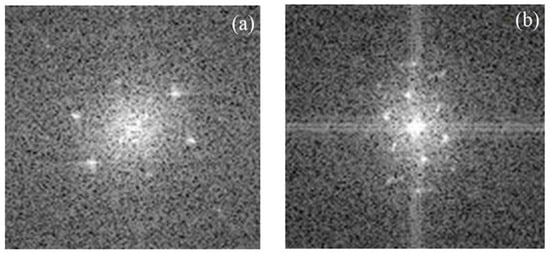
Figure 7.
The selected area electron diffraction (SAED) for Fe-FinFET (a) before and (b) after hot carrier stress.
4. Conclusions
The degradation of Ferroelectric FinFETs under different stress conditions and fin-widths, including SS degradation and hysteresis deviation, were investigated in this work. The Fe-FinFET device exhibits superior performance with narrower fins; however, it is more susceptible to device degradation under hot carrier and bias stress. From HRTEM images, the damaged Si/IL interface after hot carrier stress could be observed. As a result of voltage stress, the hysteresis of the gate ferroelectric film deteriorated, causing a transformation in its crystal properties from an orthonormal structure with lower hysteresis to an orthogonal structure with higher hysteresis. The findings suggest that during hot carrier stress, Fe-FinFET not only harms the Si/IL interface but also alters the structure of the gate ferroelectric film. SS degradation, which is linked to hysteresis deviation, is notable after HCI stress.
Author Contributions
Methodology, W.-Q.Z. and Y.-L.Y.; experiments, P.-T.W. and Y.-H.L.; writing, W.-Q.Z.; funding acquisition, Y.-L.Y.; supervision, W.-Q.Z. and Y.-L.Y. All authors have read and agreed to the published version of the manuscript.
Funding
This work was financially supported by the National Science and Technology Council in Taiwan (contract MOST 111-2221-E-017-011).
Data Availability Statement
Not applicable.
Acknowledgments
The authors would like to thank the staff of the Taiwan Semiconductor Research Institute (TSRI) for their commendable support.
Conflicts of Interest
The authors declare no conflict of interest.
References
- Salahuddin, S.; Datta, S. Use of Negative Capacitance to Provide Voltage Amplification for Low Power Nanoscale Devices Low Power Nanoscale Devices. Nano Lett. 2008, 8, 405–410. [Google Scholar] [CrossRef] [PubMed]
- Lyu, X.; Si, M.; Shrestha, P.R.; Cheung, K.P.; Ye, P.D. First direct measurement of sub-nanosecond polarization switching in ferroelectric hafnium zirconium oxide. In Proceedings of the IEEE International Electron Device Meeting, San Francisco, CA, USA, 9–11 December 2019. [Google Scholar] [CrossRef]
- Sharma, A.A.; Doyle, B.; Yoo, H.J.; Tung, I.C.; Kavalieros, J.; Metz, M.V.; Reshotko, M.; Majhi, P.; Brown-Heft, T.; Chen, Y.J.; et al. High Speed Memory Operation in Channel-Last, Back-gated Ferroelectric Transistors, In Proceedings of the IEEE International Electron Device Meeting, San Francisco, CA, USA, 12–18 December 2020. [CrossRef]
- Wang, X.; Liu, C.; Chen, Y.; Wu, G.; Yan, X.; Huang, H.; Wang, P.; Tian, B.; Hong, Z.; Wang, Y.; et al. Ferroelectric FET for nonvolatile memory application with two-dimensional MoSe2 channels. 2D Mater. 2017, 4, 025036. [Google Scholar] [CrossRef]
- Lee, C.C.; Hsieh, D.R.; Li, S.W.; Kuo, Y.S.; Chao, T.S. Hysteresis-Free Gate-All-Around Stacked Poly-Si Nanosheet Channel Ferroelectric HfxZr1-xO2 Negative Capacitance FETs With Internal Metal Gate and NH3 Plasma Nitridation. IEEE Trans. Electron Devices 2022, 69, 1512–1518. [Google Scholar] [CrossRef]
- Khan, A.I.; Keshavarzi, A.; Datta, S. The future of ferroelectric field-effect transistor technology. Nat. Electron. 2020, 3, 588–597. [Google Scholar] [CrossRef]
- Kao, M.Y.; Salahuddin, S.; Hu, C. Negative capacitance enables GAA scaling VDD to 0.5 V. Solid-State Electron. 2021, 181–182, 108010. [Google Scholar] [CrossRef]
- Gupta, A.K.; Raman, A.; Kumar, N. Design Considerations and Optimization of Electrostatic Doped Ferroelectric Nanotube Tunnel FET: Analog and Noise Analysis. Silicon 2022, 14, 10357–10373. [Google Scholar] [CrossRef]
- Solay, L.R.; Kumar, N.; Amin, S.I.; Kumar, P.; Anand, S. Design and performance analysis of gate-all-around negative capacitance dopingless nanowire tunnel field effect transistor. Semicond. Sci. Technol. 2022, 37, 115001. [Google Scholar] [CrossRef]
- Mah, S.K.; Ker, P.J.; Ahmad, I.; Zainul Abidin, N.F.; Ali Gamel, M.M. A Feasible Alternative to FDSOI and FinFET: Optimization of W/La2O3/Si Planar PMOS with 14 nm Gate-Length. Materials 2021, 14, 5721. [Google Scholar] [CrossRef] [PubMed]
- Yang, Y.L.; Zhang, W.; Yan, S.Y.; Yu, Y.H.; Fang, Z.Y.; Yeh, W.K. Study on device reliability for P-type FinFETs with different fin numbers. Vacuum 2019, 181, 109601. [Google Scholar] [CrossRef]
- Boukortt, N.E.I.; Lenka, T.R.; Patanè, S.; Crupi, G. Effects of Varying the Fin Width, Fin Height, Gate Dielectric Material, and Gate Length on the DC and RF Performance of a 14-nm SOI FinFET Structure. Electronics 2022, 11, 91. [Google Scholar] [CrossRef]
- Ko, M.D.; Sohn, C.W.; Baek, C.K.; Jeong, Y.H. Study on a Scaling Length Model for Tapered Tri-Gate FinFET Based on 3-D Simulation and Analytical Analysis. IEEE Trans. Electron Devices 2013, 60, 2721–2727. [Google Scholar] [CrossRef]
- Lin, C.L.; Hsiao, P.H.; Yeh, W.K.; Liu, H.W.; Yang, S.R.; Chen, Y.T.; Chen, K.M.; Liao, W.S. Effects of Fin Width on Device Performance and Reliability of Double-Gate n-Type FinFETs. IEEE Trans. Electron Devices 2013, 60, 3639–3644. [Google Scholar] [CrossRef]
- Ha, D.; Takeuchi, H.; Choi, Y.K.; King, T.J.; Bai, W.; Kwong, D.L.; Agarwal, A.; Ameen, M. Molybdenum-Gate HfO2 CMOS FinFET technology. In Proceedings of the IEEE International Electron Device Meeting, San Francisco, CA, USA, 13–15 December 2004. [Google Scholar] [CrossRef]
- Yan, S.C.; Wu, C.H.; Sun, C.J.; Lin, Y.W.; Yao, Y.J.; Wu, Y.C. Trench FinFET Nanostructure with Advanced Ferroelectric Nanomaterial HfZrO2 for Sub-60-mV/Decade Subthreshold Slope for Low Power Application. Nanomaterials 2022, 12, 2165. [Google Scholar] [CrossRef] [PubMed]
- De, S.; Aftab Baig, M.; Qiu, B.H.; Müller, F.; Le, H.H.; Lederer, M.; Kämpfe, T.; Ali, T.; Sung, P.J.; Su, C.J.; et al. Random and Systematic Variation in Nanoscale Hf0.5Zr0.5O2 Ferroelectric FinFETs: Physical Origin and Neuromorphic Circuit Implications. Front. Nanotech. 2021, 3, 826232. [Google Scholar] [CrossRef]
- Yeh, W.K.; Zhang, W.; Chen, P.Y.; Yang, Y.L. The Impact of Fin Number on Device Performance and Reliability for Multi-Fin Tri-Gate n- and p-type FinFET. IEEE Trans. Device Mater. Reliab. 2018, 18, 555–560. [Google Scholar] [CrossRef]
- Yang, Y.L.; Zhang, W.; Yeh, Y.K. Study on Intrinsic Hot Carrier Degradation of FinFETs with Different Stress Conditions and Fin Numbers by Decoupling PBTI Component. ECS J. Solid State Sci. Technol. 2020, 9, 033006. [Google Scholar] [CrossRef]
- Yeh, W.K.; Yang, L.Q.; Shen, C.H.; Kong, C.H.; Tseng, P.Y.; Yang, Y.L. Study on Negative Bias Temperature Instability Induced Degradation of P-Type FinFETs by Distinguishing Fin Top and Fin Sidewalls. ECS J. Solid State Sci. Technol. 2022, 11, 065005. [Google Scholar] [CrossRef]
- De, S.; Lu, D.D.; Le, H.H.; Mazumder, S.; Lee, Y.J.; Tseng, W.C.; Qiu, B.H.; Baig, M.A.; Sung, P.J.; Su, C.J.; et al. Ultra-Low Power Robust 3bit/cell Hf0.5Zr0.5O2 Ferroelectric FinFET with High Endurance for Advanced Computing-In-Memory Technology. In Proceedings of the Symposium on VLSI Technology, Kyoto, Japan, 13–19 June 2021; Available online: https://ieeexplore.ieee.org/document/9508674 (accessed on 11 August 2021).
- Wang, H.; Yang, M.; Huang, Q.; Zhu, K.; Zhao, Y.; Liang, Z.; Chen, C.; Wang, Z.; Zhong, Y.; Zhang, X.; et al. New Insights into the Physical Origin of Negative Capacitance and Hysteresis in NCFETs. In Proceedings of the IEEE International Electron Device Meeting, San Francisco, CA, USA, 1–5 December 2018. [Google Scholar] [CrossRef]
- Koval, V.; Viola, G.; Tan, Y. Biasing Effects in Ferroic Materials. In Ferroelectric Materials-Synthesis and Characterization; IntechOpen: London, UK, 2015. [Google Scholar] [CrossRef]


Disclaimer/Publisher’s Note: The statements, opinions and data contained in all publications are solely those of the individual author(s) and contributor(s) and not of MDPI and/or the editor(s). MDPI and/or the editor(s) disclaim responsibility for any injury to people or property resulting from any ideas, methods, instructions or products referred to in the content. |
© 2023 by the authors. Licensee MDPI, Basel, Switzerland. This article is an open access article distributed under the terms and conditions of the Creative Commons Attribution (CC BY) license (https://creativecommons.org/licenses/by/4.0/).