Abstract
The physical properties of silicon carbide (SiC) are excellent as a third-generation semiconductor. Nevertheless, diamond wire cutting has many drawbacks, including high loss, long cutting time and prolonged processing time. The study of 4H-SiC wafer slicing by using an ultrafast laser is hopeful for solving these problems. In this work, the 4H-SiC samples with different surface roughness were processed by laser slicing. Findings revealed that good surface quality could reduce the damage to the wafer surface during laser slicing, reduce cleavage, and improve the flatness and uniformity of the modified layer. Thus, preprocessing on 4H-SiC can significantly improve the quality and efficiency of laser slicing.
1. Introduction
Silicon carbide (SiC), a typical third-generation wide-bandgap semiconductor material, has excellent physical properties, including high thermal conductivity, high breakdown electric field, and high electron saturation rates [1]. Therefore, SiC has found widespread use in a wide range of applications, from single crystals, epitaxial materials, power devices, and high-power modules. As a result of its hardness and friability, its application is limited by the cost of wafer production. It is common practice today to produce wafers with the dicing saw method [2]; although this technique is suitable for mass wafer production, it can result in problems such as chipping, cracking, and heating. Moreover, it leads to low throughput and high-process costs. For example, the slicing of 6-inch SiC ingot requires 100 h, and one 6-inch SiC wafer may cause approximately 160 μm loss in the slicing process. The surface of the cutting piece may also have more severe damage, resulting in poor surface quality and higher application cost.
Researchers are investigating how to apply laser technology to slice SiC wafers from ingots. As a result of laser slicing, a modified layer is formed across the entire surface of the SiC ingots. The formation of the modified layer is mainly carried out by photon injection [3], and an automatic system can control it to adjust the laser parameters. Nowadays, femtosecond pulsed laser processing is well-established in stealth dicing, which uses laser energy to reach the damage threshold of SiC for wafer slicing [4], as well as a variety of detection methods, such as acoustic emission, have been proposed [5]. Using a laser on SiC, photons are used to excite the free electrons in the valence band, thereby causing them to leap into the conduction band. Low laser intensity results in low photon energy. The main mechanism is to continue impact ionization by exciting free electrons as seed electrons, increasing the number of conduction band electrons, and producing avalanche ionization. A high laser intensity causes multiphoton ionization and tunnel ionization to occur. Compared to picosecond lasers, femtosecond lasers have short pulse times and high peak power, enabling rapid energy delivery, avoiding thermal processing effects due to thermal diffusion, and enabling high-quality surface quality [6,7]. Because femtosecond laser pulses are shorter than picosecond laser pulses, the lattice temperature will not be significantly affected by the femtosecond laser when it acts on silicon carbide crystals inside [8], as it would with a picosecond laser. Through carrier-phonon scattering [9], the crystal’s interior will be in an equilibrium state due to the rapid increase in carriers [10], eventually reaching equilibrium within picoseconds [11]. Femtosecond lasers have wide application prospects in the laser stripping of 4H-SiC wafers. EUNHO KIM et al. [12,13] proposed a femtosecond double-pulse stripping of 4H-SiC and investigated the impact of the pulse width on the expansion of the reformer layer inside the 4H-SiC crystal and achieved the stripping of 5 × 5 mm samples. Kazuya Hirata et al. [14] later reported a femtosecond laser slicing method called KABRA and demonstrated that the femtosecond laser caused elemental changes within 4H-SiC and enabled the stripping and commercialization of large-size 4H-SiC wafers. Marko Swoboda et al. [15,16] used a low-temperature cold cracking method for the stripping of 4H-SiC wafers based on laser action and introduced a cold cracking peeling method for 4H-SiC and integrated it with wafer production. Han, Shifei et al. [17] investigated laser-induced microbursts for 4H-SiC exfoliation with picosecond lasers. However, in recent years, there are a lack of relevant reports on the quality of the modified layer and the pretreatment of the surface of the ingot.
The leading goal of this paper is to investigate the impact of surface preprocessing on the slicing of 4H-SiC wafers using an ultrafast laser. In this work, we used four 10 × 10 × 1 mm 4H-SiC samples with roughness ranging from 0.5 to 500 nm, and then experimented with a femtosecond laser system to form the modified layer. Finally, the wafer is sliced by a tensile machine. This paper also characterized the morphology of a modified layer by microscopic observation, LEXT, X-ray spectra, Raman spectra and EDS.
2. Experimental Equipment and Material
A high-purity 4H-SiC wafer was produced using a physical vapor transmission method and cut into four squares of 10 × 10 × 1 mm. The microscopic observations of sample surfaces are displayed in Figure 1a–d. Figure 2 shows that four samples with different roughness ranges from 500 to 0.5 nm, with sample (1) being the unprocessed sample with a roughness of 500 nm, and its surface displaying noticeable line marks due to the influence of diamond wire cutting. Sample (2) was processed by polishing, and the line mark becomes shallow but the surface is still rough with a roughness of 250 nm. Sample (3) was processed by mechanical polishing, and its surface quality has been greatly improved, but there are still some scratches on the surface, and its roughness is about 20 nm. Sample (4) was processed by chemical mechanical polishing; its roughness is about 0.5 nm, and there is no scratch on the surface.

Figure 1.
Surface of the samples after different processing methods. (a) Sample 1 with the surface after wire cutting. (b) Sample 2 with the surface after polishing. (c) Sample 3 with the surface after mechanical polishing. (d) Sample 4 with the surface after chemical mechanical polishing.
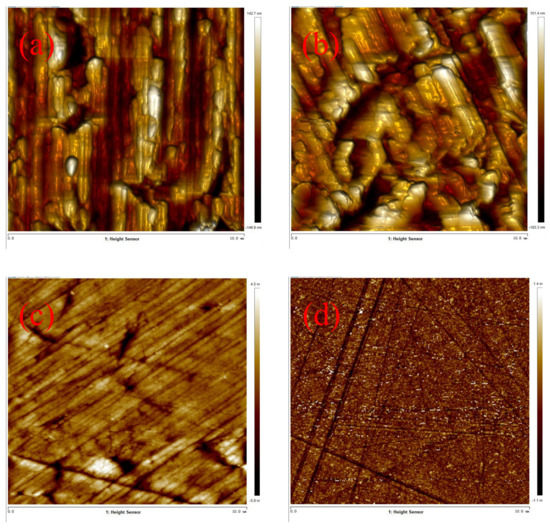
Figure 2.
AFM of the surface of the samples after different process methods. (a) Sample 1 with the surface after wire cutting. (b) Sample 2 with surface after polishing. (c) Sample 3 with the surface after mechanical polishing. (d) Sample 4 with surface after chemical mechanical polishing.
Then, four samples were processed by a femtosecond laser. The parameters of the femtosecond laser system were set as: The laser wavelength was 1030 nm, the spot radius was 10 μm, the repetition frequency was 1~100 khz, the pulse width was 500 fs, M2 < 1.2, and the maximum laser energy was E = 10 μ J. The moving speed of the processing platform was 100–200 mm/s. Figure 3 shows the schematic diagram of the laser system. The laser beam is focused on the 4H-SiC wafer through a 20× objective lens. The peak power density is 9.9 × 10¹⁸ W/cm2. The tensile strength was applied to the sample by an electronic universal tensile machine to slice the wafer. In the end, the wafers were sliced, and the surface roughness was tested by an atomic force microscope (Brucker). For studying 4H-SiC structural changes and element changes, Raman spectrometry (Horiba-HR800), X-ray (Brucker-D8-DISCOVER), and scanning electron microscope (Pioneer Two) were used.

Figure 3.
Schematic diagram of the femtosecond laser system.
3. Results
3.1. H-SiC Absorption Spectrum Test
Absorption properties of 4H-SiC are important when choosing the femtosecond laser wavelength. It has an essential influence on the absorption of laser energy, the thickness of the modified layer, and the surface quality after processing. We used a spectroscope to analyze the absorption spectrum of 4H-SiC. As shown in Figure 4, when the wavelength is 1030 nm, the absorption rate of 4H-SiC is the lowest, about 0.5%. Controlling the femtosecond laser wavelength can reduce the absorption of 4H-SiC to laser energy and improve surface quality after processing.
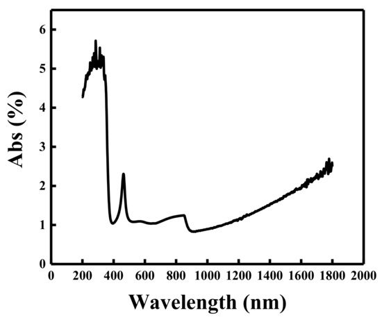
Figure 4.
The absorption spectrum of 4H-SiC.
3.2. Effect of Surface Preprocessing on Surface Damage and Modified Layer
To investigate the damage threshold caused by different surface preprocessing after laser processing, we use the single-pulse laser with the same pulse energy and scanning speed to form the modified layer. As shown in Figure 5a,b, it can be seen that there are obvious laser ablation marks on the surfaces of Sample (1) and Sample (2) because the surface of the SiC absorbs the laser energy. During the laser process, most energy is applied to transform the 4H-SiC to another phase and deformation on the surface. To compare the results, it is shown in Figure 5c that there was energy absorption in the scratched area, and this reduced the surface quality and the effect of laser modification. However, after femtosecond processing, Sample (4) has no ablation phenomenon, as shown in Figure 5d. This shows that the surface quality of the sample before laser processing has an important influence on the absorption of laser energy. When the surface of the sample is rough, the laser energy is constantly reflected and absorbed on the surface due to the diffuse reflection of the light beam. As a result of the pulse energy, the laser-induced electron explosion occurs on the surface of 4H-SiC, and the temperature of the surface crystal rises rapidly. Silicon vapor is produced, which makes the surface carbonized and blackened in the air. Therefore, there is no stable modified layer in 4H-SiC, as shown in Figure 6a,b. The laser energy lost by the laser at the interface between air and 4H-SiC is significantly reduced when the sample’s surface quality is improved by mechanical polishing or chemical mechanical polishing, and through refraction, the laser energy penetrates the 4H-SiC, resulting in a stable modified layer.
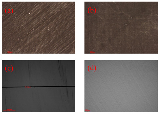
Figure 5.
The laser-treated surface of the samples after different process methods. (a) Sample 1 with the surface after wire cutting. (b) Sample 2 with the surface after polishing. (c) Sample 3 with the surface after mechanical polishing. (d) Sample 4 with the surface after chemical mechanical polishing.
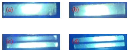
Figure 6.
The cross-sectional view of the modified layer. (a) Sample 1 with the surface after wire cutting. (b) Sample 2 with the surface after polishing. (c) Sample 3 with the surface after mechanical polishing. (d) Sample 4 with the surface after chemical mechanical polishing.
3.3. Tensile Test after the Laser Processing
In a universal tensile testing machine, both sides of the laser-processed samples were fixed to the fixtures with epoxy resin adhesive, which is shown in Figure 7a, and the tensile force was applied perpendicular to their surface direction.
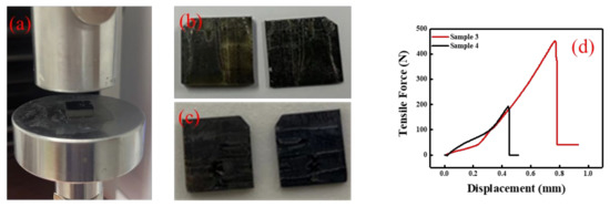
Figure 7.
Tensile stripping experiment diagram. (a) The diagram of tensile test. (b) Sample 3 after the tensile test. (c) Sample 4 after the tensile test. (d) The relationship between surface preprocessing and tensile force.
After the tensile test, sample (1) and sample (2) failed to achieve the separation with tensile force increases because the rough surface absorbed the laser energy and made it fail to form a stable modified layer. As shown in Figure 7b, sample 3 was successfully separated into two wafers. Figure 7c shows the successful separation of sample 4. Figure 7d shows the tensile stress when sample (3) and sample (4) were separated, and it can be seen that when the tensile force increased to 189 N, sample (4) was stripped off, and when the tensile force increased to 450 N, sample (3) was stripped off. The difference between the tensile force shows that the surface preprocessing plays a vital role in the tensile test, and the reduction in surface roughness helps to reduce the loss of energy, making the distribution of the modified layer more uniform to lower the tensile force required for separation.
The sample surface was then observed under an optical microscope. As shown in Figure 8, we can see evident femtosecond laser scanning traces on the stripping interface, and there is a large bright area on the stripping interface. This section is probably due to the cleavage inside the 4H-SiC along with the <001> direction. Figure 8a–c show that when the stripping surface of the sample (3) was observed, a large area of the cleavage region was observed, which was believed to be due to the absorption of laser energy by surface scratches, failing to achieve the power density required for the modified layer. Different from stripping from the modified layer, the cleavage surface had lower roughness and no laser scanning lines. After that, we analyzed the stripping interface of sample 3 with a laser confocal microscope. As shown in Figure 9, there is an obvious height difference of about 20–40 μm in the stripping interface, which is the result of the joint action of cleavage and modification. When the laser was applied to the sample, the scratches in the surface caused the difference in absorbed energy in different areas of the sample and formed a modified layer with different thicknesses. A tensile test was followed by stripping along the cleavage plane of the area with uneven distribution of the modified layer.
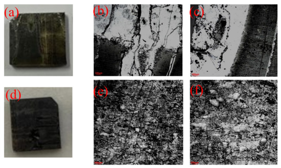
Figure 8.
The microscopic observation of the stripping interface. (a–c) Sample-3 (d–f) sample-4.
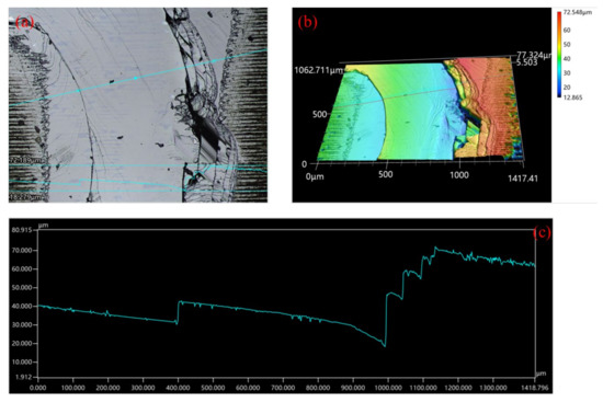
Figure 9.
The observation by laser confocal microscope of sample 3. (a) Microscope view; (b) 3D view; (c) schematic diagram of step height difference.
3.4. The Morphologies Test of the Modified Layer and Cleavage Area
The previous test revealed that the modification effect does not work out completely in sample 3. To explore the effect of the surface processing on the occurrence of the cleavage, the X-ray spectrum of the incidence plane is shown in Figure 10b, where the black curve represents the regular area of the incidence plane where the internal modification occurs, and the other curves represent the area where the internal cleavage occurs. The curve of the normal area has one peak located at 18.292°, which stands for the deflection angle of 4H-SiC, and its narrow FWHM shows the good quality of the 4H-SiC crystal. The other curves of the cleavage area have peaks located at 18.285°, 18.289°, and 18.287°, and their FWHMs are about 66.1, 70.8, and 84.4 arcsec. Compared with the normal area, the FWHMs of the cleavage area are broadened, and the peak intensity was weakened, which indicates the decrease in crystal quality of this area. The decrease in crystal quality may be related to the residual tensile stress exerted by the tensile test. As shown in Figure 7d, the cleavage area is proportional to the tension required for stripping. With the increase in tension, the residual stress acting on the cleavage region increases and causes a decrease in the crystal quality of this area.
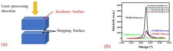
Figure 10.
(a) Schematic diagram of test surface. (b) The X-ray double crystal diffraction rocking curve of the normal area and cleavage area of the incidence plane.
Figure 11a,b shows the view of the morphologies of the modified layer with an optic microscope and scanning electron microscope. The modified lines with uneven thickness can be observed, and it can be seen from the top section that the lateral crack at each modified line was connected to form the modified layer for cracking. The modified layer can be separated by transverse crack propagation without additional tension during the tensile test.
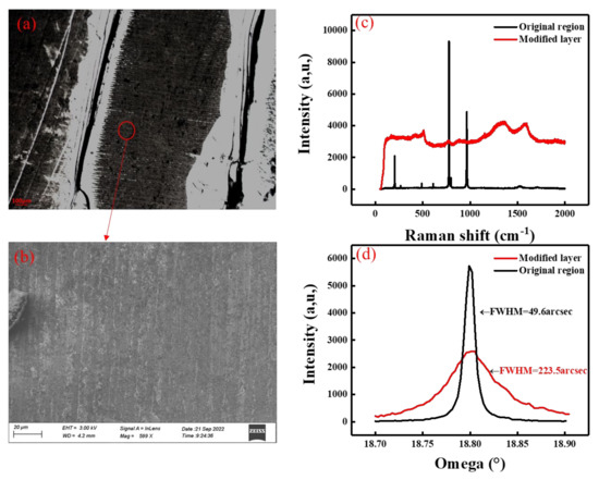
Figure 11.
(a) The microscopic observation of the modified layer. (b) SEM image of the modified layer. (d) Raman spectrum of the modified layer. (c) X-ray double crystal diffraction rocking curve of the modified layer.
The Raman spectrum of the modified layer and original region is shown in Figure 11c, where the black curve represents the original region, and the red curve represents the modified layer. We used Raman spectroscopy with an excitation wavelength of 532 nm to characterize the change in the peeling surface structure. Based on the spatial symmetry C46v of single crystal 4H-SiC, with an excitation Raman wavelength of 532 nm, the peaks of the original region at 205, 610, 778, 798, 965 cm−1 are assigned to its unique phonon mode. Compared with the original region without modification, the intensity of the peak at 778 cm−1 was weakened and the FWHM was broadened, which improved the crystal in the modified layer and has been modified to an amorphous state. In addition, the peaks at 480 cm−1 show the appearance of amorphous carbon [18], and the peaks at 1200 and 1600 cm−1 show the appearance of amorphous silicon. The result shows that the effect of modification is to transform the 4H-SiC to amorphous carbon and amorphous under laser processing.
The X-ray double crystal diffraction rocking curve of the modified layer is shown in Figure 11d, where the black curve represents the original region, and the red curve represents the modified layer. Compared with the original region without modification, the intensity of the peak of the SiC in the modified layer was weakened, and the FWHM was broadened, which indicated the silicon carbide crystal in the modified layer had been damaged and the occurrence of a damaged layer.
The views of the morphologies of the cleavage region with an optic microscope and scanning electron microscope are shown in Figure 12a,b. The generation of cleavage area is the main reason for the increase in the tension required for peeling in the tensile test. The smooth surface of the cleavage region can be observed, which is due to the fracture in the silicon carbide single crystal along the weakest direction of the chemical bond. The height difference of the cleavage plane can be observed in Figure 12b.
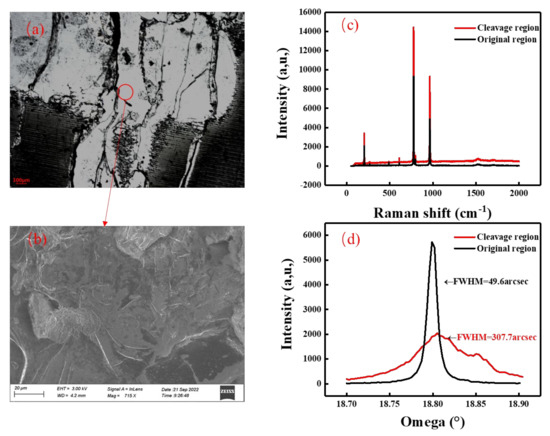
Figure 12.
(a) The microscopic observation of the cleavage area. (b) SEM image of the cleavage area. (c) Raman spectrum of the cleavage region. (d) X-ray double crystal diffraction rocking curve of the cleavage region.
The Raman spectrum of the cleavage region and original region is shown in Figure 12c, where the black curve represents the original region, and the red curve represents the cleavage region. It indicated that the main component of the cleavage region is still SiC crystal, which improves the modification and does not work out in the cleavage region.
The X-ray double crystal diffraction rocking curve of the cleavage region is shown in Figure 12d, where the black curve represents the original region, and the red curve represents the cleavage region. Compared with the original region, the intensity of the peak of SiC in the cleavage was weakened and FWHM was broadened, which indicated the silicon carbide crystal in the modified layer has been damaged and the occurrence of a damaged layer. In addition, as shown in Figure 10b, Figure 11d and Figure 12d, the FWHM of the cleavage region is also broader than the modified layer, which indicates the crystal quality of the cleavage region is worse than the modified layer in the stripping surface, which is believed to be due the fact that the tensile force is mainly acting on the cleavage region, and it makes the large residual stress remain in the cleavage region.
3.5. Elemental Analysis of Stripping Interface
EDS element analysis was carried out on the stripped surface. It can be seen from Figure 13 that the main elements of the stripped surface are the Si element and the C element. Compared with the stealth cutting of 4H-SiC, no O element enters the crystal because the modification reaction takes place in the interior, which also proves that the function of the femtosecond laser is to cause the bond-breaking reaction of internal 4H-SiC.
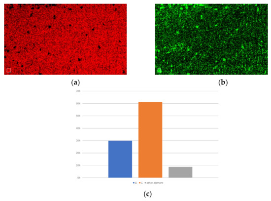
Figure 13.
EDS element analysis of stripping surface. (a)Si element distribution, (b) C element distribution, (c) atomic proportion of exfoliation surface.
4. Conclusions
In this paper, four 4H-SiC samples with a roughness of 0.5, 20, 250, and 500 nm were processed by a femtosecond laser to investigate the influence of surface preprocessing on wafer slicing. Surface preprocessing is able to reduce the surface damage by laser processing and promote the stable formation of the modified layer, reducing the ratio of the area of cleavage and reducing the tension required for wafer slicing. In summary, the surface preprocessing of 4H-SiC is helpful in improving the quality of wafer slicing by using an ultrafast laser.
Author Contributions
H.W.: investigation, formal analysis, data curation, writing—original draft preparation. Q.C. and Y.Y.: writing—review and editing, validation, software. L.C.: visualization. B.Z. and H.N.: validation, supervision. R.W.: funding acquisition, supervision, project administration. All authors have read and agreed to the published version of the manuscript.
Funding
This work was financially supported by the National Natural Science Foundation of China (52022052, 62004118) and The Fundamental Research Funds of Shandong University (2020GN080).
Data Availability Statement
Not applicable.
Acknowledgments
The authors sincerely thank Rongkun Wang for his great time and effort in the preparation and revising of the manuscript and thank Xian Gang Xu for his theoretical support and help in this work.
Conflicts of Interest
The authors declare that they have no known competing financial interests or personal relationships that could have appeared to influence the work reported in this paper.
References
- Kirschman, R. Status of Silicon Carbide (SiC) as a WideBandgap Semiconductor for High Temperature Applications: A Review. Solid-State Electron. 1996, 39, 1409–1422. [Google Scholar] [CrossRef]
- Dohnke, K.O.; Kaspar, K.; Lewke, D. Comparison of Different Novel Chip Separation Methods for 4H-SiC. Mater. Sci. Forum 2015, 821–823, 520–523. [Google Scholar] [CrossRef]
- Ohmura, E.; Fukuyo, F.; Fukumitsu, K.; Morita, H. Internal modified-layer formation mechanism into silicon with nanosecond laser. J. Achiev. Mater. Manuf. Eng. 2006, 17, 381–384. [Google Scholar] [CrossRef]
- Wang, L.; Zhang, C.; Liu, F.; Zheng, H.; Cheng, G.J. Process mechanism of ultrafast laser multi-focal-scribing for ultrafine and efficient stealth dicing of SiC wafers. Appl. Phys. A 2022, 128, 872. [Google Scholar] [CrossRef]
- Xie, X.; Zhang, Y.; Huang, Q.; Huang, Y.; Zhang, W.; Zhang, J.; Long, J. Monitoring method for femtosecond laser modification of silicon carbide via acoustic emission techniques. J. Mater. Process. Technol. 2020, 290, 116990. [Google Scholar] [CrossRef]
- Fukuyo, F.; Fukumitsu, K.; Uchiyama, N. The Stealth Dicing Technologies and Their Application. In Proceedings of the 6th International Symposium on Laser Precision Microfabrication, Williamsburg, VA, USA, 4–8 April 2005. [Google Scholar]
- Zhang, Z.; Wen, Z.; Shi, H.; Song, Q.; Xu, Z.; Li, M.; Hou, Y.; Zhang, Z. Dual laser beam asynchronous dicing of 4H-sic wafer. Micromachines 2021, 12, 1331. [Google Scholar] [CrossRef] [PubMed]
- Bulgakova, N.M.; Burakov, I.M.; Meshcheryakov, Y.P.; Stoian, R.; Rosenfeld, A.; Hertel, I.V. Theoretical models and qualitative interpretation of fs laser material processing. J. Laser Micro/Nano Eng. 2007, 2, 76–86. [Google Scholar] [CrossRef]
- Jiang, L.; Tsai, H.L. Energy transport and material removal in wide bandgap materials by a femtosecond laser pulse. Int. J. Heat Mass Transf. 2005, 48, 487–499. [Google Scholar] [CrossRef]
- Pecholt, B.; Vendan, M.; Dong, Y.; Molian, P. Ultrafast laser micromachining of 3C-SiC thin films for MEMS device fabrication. Int. J. Adv. Manuf. Technol. 2008, 39, 239–250. [Google Scholar] [CrossRef]
- Rethfeld, B.; Sokolowski-Tinten, K.; Von Der Linde, D.; Anisimov, S.I. Timescales in the response of materials to femtosecond laser excitation. Appl. Phys. A 2004, 79, 767–769. [Google Scholar] [CrossRef]
- Kim, E.; Shimotsuma, Y.; Sakakura, M.; Miura, K. Ultrashort Pulse Laser Slicing of Wide Bandgap 4H-SiC Crystal. In JSAP-OSA Joint Symposia 2016 Abstracts; Optica Publishing Group: Washington, DC, USA, 2016. [Google Scholar]
- Kim, E.; Shimotsuma, Y.; Sakakura, M.; Miura, K. 4H-SiC wafer slicing by using femtosecond laser double-pulses. Opt. Mater. Express 2017, 7, 2450–2460. [Google Scholar] [CrossRef]
- Hirata, K. New Laser Slicing Technology Named KABRA Process Enables High Speed and High Efficiency SiC Slicing. In Proceedings of the Conference on Laser-Based Micro- and Nanoprocessing, Tokyo, Japan, 30 January–1 February 2018. [Google Scholar]
- Swoboda, M.; Beyer, C.; Rieske, R.; Drescher, W.; Richter, J. Laser assisted sic wafer using cold split. Mater. Sci. Forum 2017, 897, 403–406. [Google Scholar] [CrossRef]
- Swoboda, M.; Rieske, R.; Beyer, C.; Ullrich, A.; Gesell, G.; Richter, J. Cold Split Kerf-Free Wafering Results for Doped 4h-Sicboules. Mater. Sci. Forum 2019, 963, 10–13. [Google Scholar] [CrossRef]
- Han, S.; Yu, H.; He, C.; Zhao, S.; Ning, C.; Jiang, L.; Lin, X. Laser slicing of 4h-sic wafers based on picosecond laser-induced micro-explosion via multiphoton processes. Opt. Laser Technol. 2022, 154, 108323, ISSN 0030-3992. [Google Scholar] [CrossRef]
- Dresselhaus, M.S.; Jorio, A.; Hofmann, M.; Dresselhaus, G.; Saito, R. Perspectives on Carbon Nanotubes and Graphene Raman Spectroscopy. Nano Lett. 2010, 10, 751–758. [Google Scholar] [CrossRef] [PubMed]


Disclaimer/Publisher’s Note: The statements, opinions and data contained in all publications are solely those of the individual author(s) and contributor(s) and not of MDPI and/or the editor(s). MDPI and/or the editor(s) disclaim responsibility for any injury to people or property resulting from any ideas, methods, instructions or products referred to in the content. |
© 2022 by the authors. Licensee MDPI, Basel, Switzerland. This article is an open access article distributed under the terms and conditions of the Creative Commons Attribution (CC BY) license (https://creativecommons.org/licenses/by/4.0/).