Article

Effects of Different Anti-Solvents and Annealing Temperatures on Perovskite Thin Films

1
Institute of Microelectronics, Department of Electrical Engineering, National Cheng-Kung University, Tainan 70101, Taiwan
2
Department of Applied Physics, National University of Kaohsiung, Kaohsiung University Rd., Kaohsiung 81148, Taiwan
*
Author to whom correspondence should be addressed.
Crystals 2022, 12(8), 1074; https://doi.org/10.3390/cryst12081074
Submission received: 8 July 2022 / Revised: 26 July 2022 / Accepted: 29 July 2022 / Published: 31 July 2022
(This article belongs to the Special Issue Solution-Based Processes in Semiconductors and Electronic Devices)

Abstract

:
Since perovskite materials are currently mostly used in the active layer of solar cells, how to maximize the conversion efficiency of the active layer is the most urgent problem at present. In this regard, the extremely low voltage loss and tunable energy gap of methyl lead iodide (MAPbI3) perovskites make them very suitable for all perovskite solar cell applications, and are also compatible with silicon crystalline systems. Therefore, the future development of MAPbI3 perovskite will be very important. The key point of film formation in MAPbI3 is the addition of anti-solvent, which will affect the overall quality of the film. Whether it can be used as an excellent active layer to improve the application value will be very important. Therefore, the research purpose of this topic “Effects of different anti-solvents and annealing temperatures on perovskites” is to complete the basic research and development of a light-absorbing layer of a solar cell element, in which three different anti-solvents need to be matched with each other as the active light-absorbing layer of a solar cell. Through optimization, using the chemical properties of different anti-solvents and different annealing temperatures, combined with the low-process-cost characteristics of organic materials and many other advantages, we researched the optimized process methods and parameters to improve the absorption efficiency of the active light-absorbing layer.

1. Introduction

In the past few years, the maximum power conversion efficiency (PCE) of perovskite solar cells (PSCs) has rapidly increased from 3% to 25.6% [1,2,3,4,5,6]. Its conversion efficiency is close to that of crystalline silicon solar cells, showing great industrial prospects. In order to improve the application performance of perovskite cells, research mainly focuses on the preparation technology of high-quality perovskite thin films. The precise control of the parameters and growth conditions of perovskite thin films is a key way to fabricate high-quality perovskite solar cells and explore fundamental properties [7,8,9]. The surface morphology, coverage, and grain size of perovskite thin films are the key factors affecting the battery performance.
However, organic–inorganic metal halide perovskites’ band gaps (1.16–3.06 eV) are easy to tune, and they have good optical and electronic properties, efficient charge transport, high light-absorption properties, long diffusion lengths, and a low-cost solution. Based on the above advantages, meaning they are considered to be the most promising third-generation low-cost solar cells [10,11,12]. The perovskite methylamine lead triiodide (CH3NH3PbI3; MAPbI3) has been extensively studied due to its excellent power conversion efficiency, high quantum yield, low-cost fabrication, and remarkable absorbance properties [13,14,15,16,17]. However, MAPbI3 is easily degraded to PbI2 in steam and air, and will affect the research of efficient perovskite solar cells. Therefore, improving the performance of hybrid perovskite MAPbI3 thin films has been the main research direction in recent years [18,19,20,21,22]. The current research efforts are mainly focused on reducing toxicity, optimizing the manufacturing process, and improving efficiency and stability. Among the most commonly used methods, due to the simplicity of fabrication and ease of use and the low cost, the one-step solution method is often used for perovskite deposition. Two-step vapor-assisted deposition can well control the film surface and particle size. Thermal vapor deposition is often used to fabricate thin films with regular thickness. However, it is difficult to accurately control the composition of the film owing to an uncontrollable precursor. The single-step solution deposition method usually uses an anti-solvent to remove N,N-dimethylformamide (DMF) in the precursor solution which can make the solution supersaturate and form large and dense homogeneous perovskite films. The common anti-solvents are toluene, chlorobenzene, etc. However, perovskite materials still have some shortcomings, such as degradation, owing to combing with water and poor thermal stability. The method with the most potential is using thermal annealing to make the film stronger and denser. In this study, o-dichlorobenzene, chlorobenzene, and toluene were used as an anti-solvent for removing excess precursor. The temperature optimization for perovskite thin films was performed using post-annealing treatment.

2. Materials and Methods

2.1. Synthesis of CH3NH3PbI3

We added CH3NH3I (198.75 mg) and PbI2 (576.25 mg) into the 50 mL sample bottle, and then added dimethyl sulfoxide (C2H6OS; DMSO) (0.5 mL) and 1,4-dihydroxybenzene (C6H6O2; GBL) (0.5 mL) into the sample bottle in the glove box and stirred at 300 rpm for 24 h.

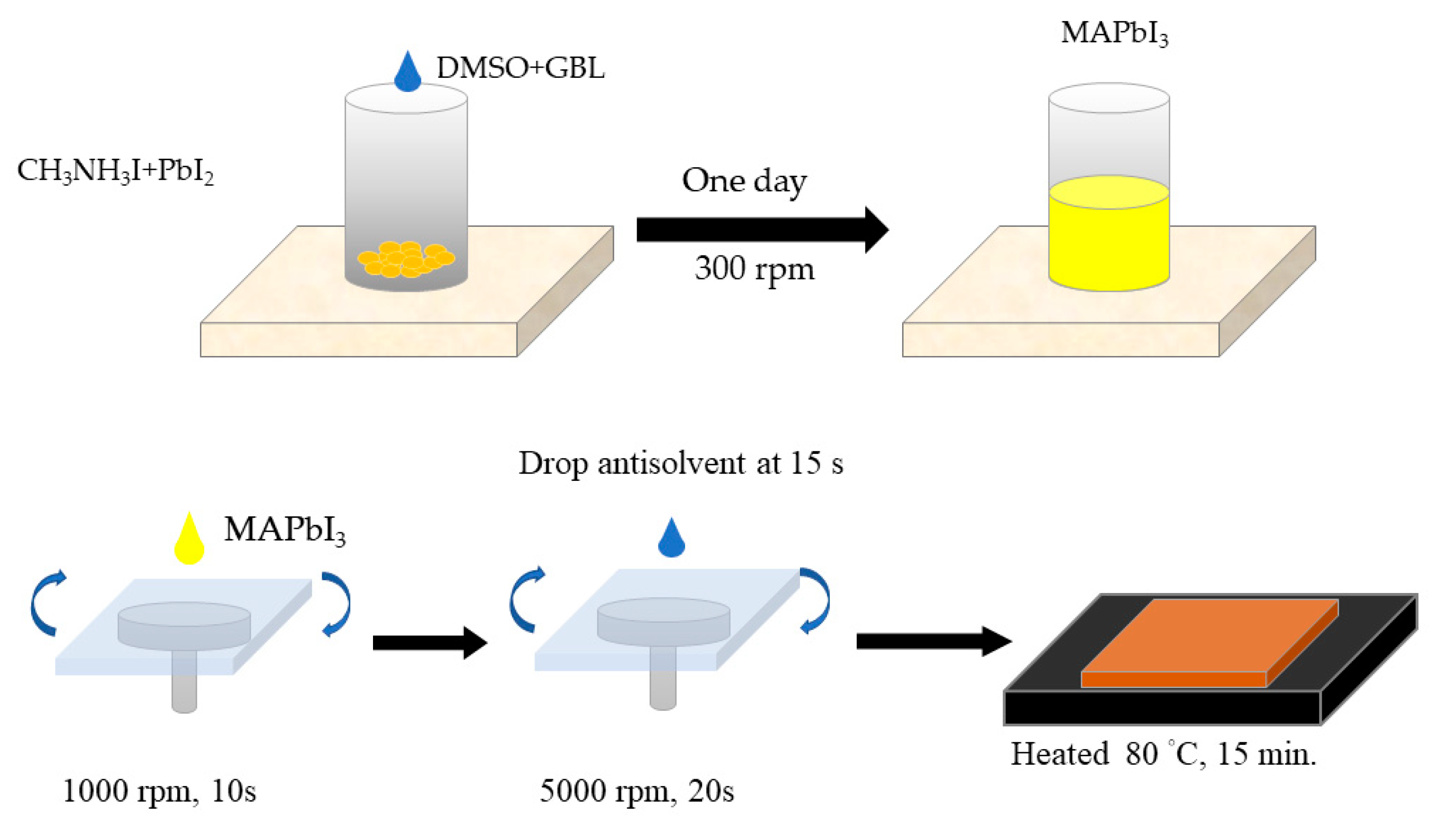
2.2. Fabrication of Thin Films

CH3NH3PbI3 (50 μL) spin-coated on the glass substrate in the glove box, then filmed by different filming temperatures from 80 °C, as shown in Figure 1. After film formation, re-annealing was performed in a tubular furnace.

2.3. Characteristic Measurements

The absorption spectra of the thin film were measured by ultraviolet/visible (UV/vis) absorption spectroscopy (HITACHI, U-3900, Tokyo, Japan). X-ray diffraction data of films were recorded by the Bruker D8 Discover X-ray diffractometer with Grazing Incidence X-Ray Diffraction (GIXRD; Bruker, D8 Discover, Billerica, MA, USA).

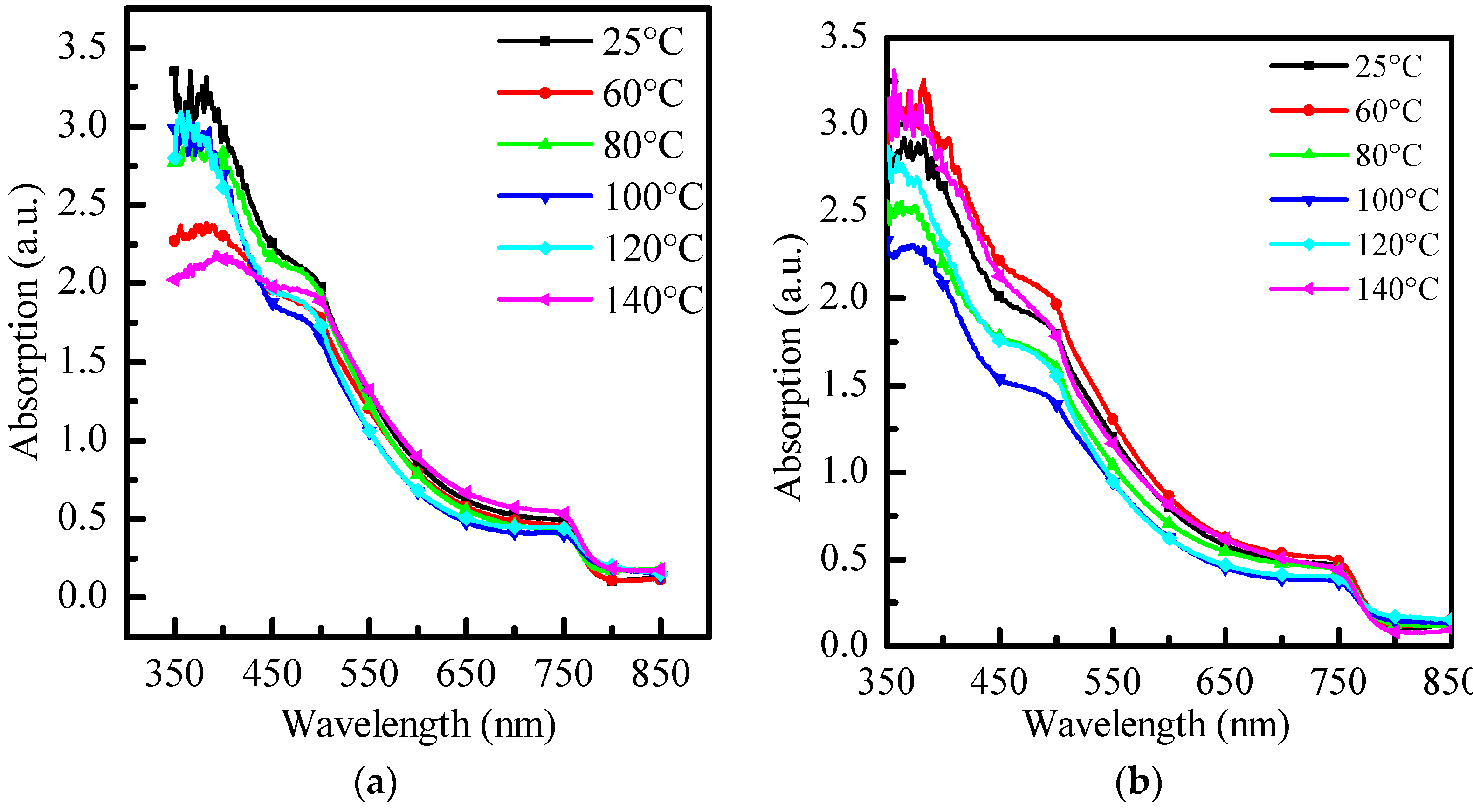
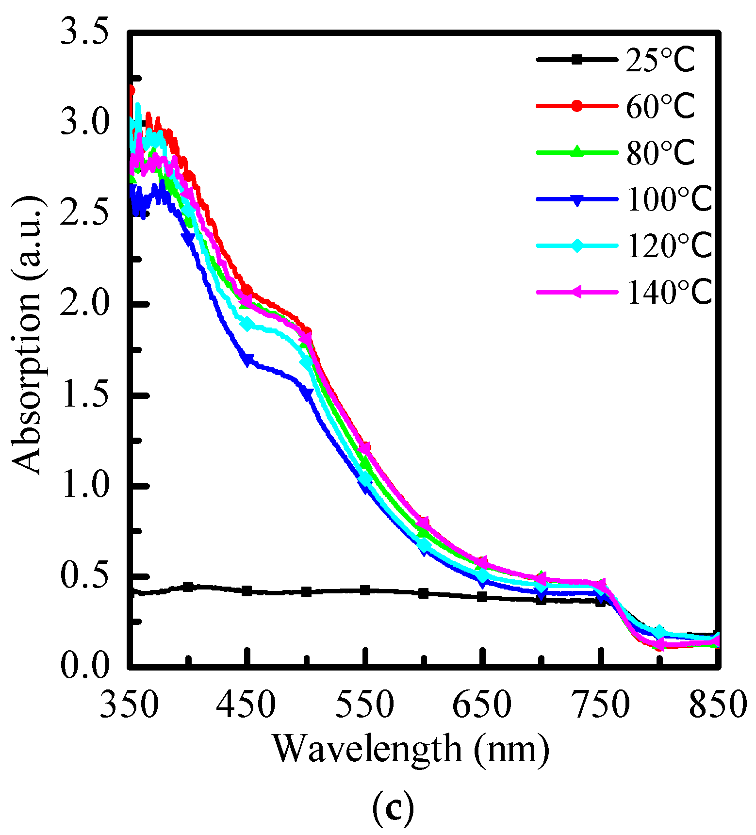
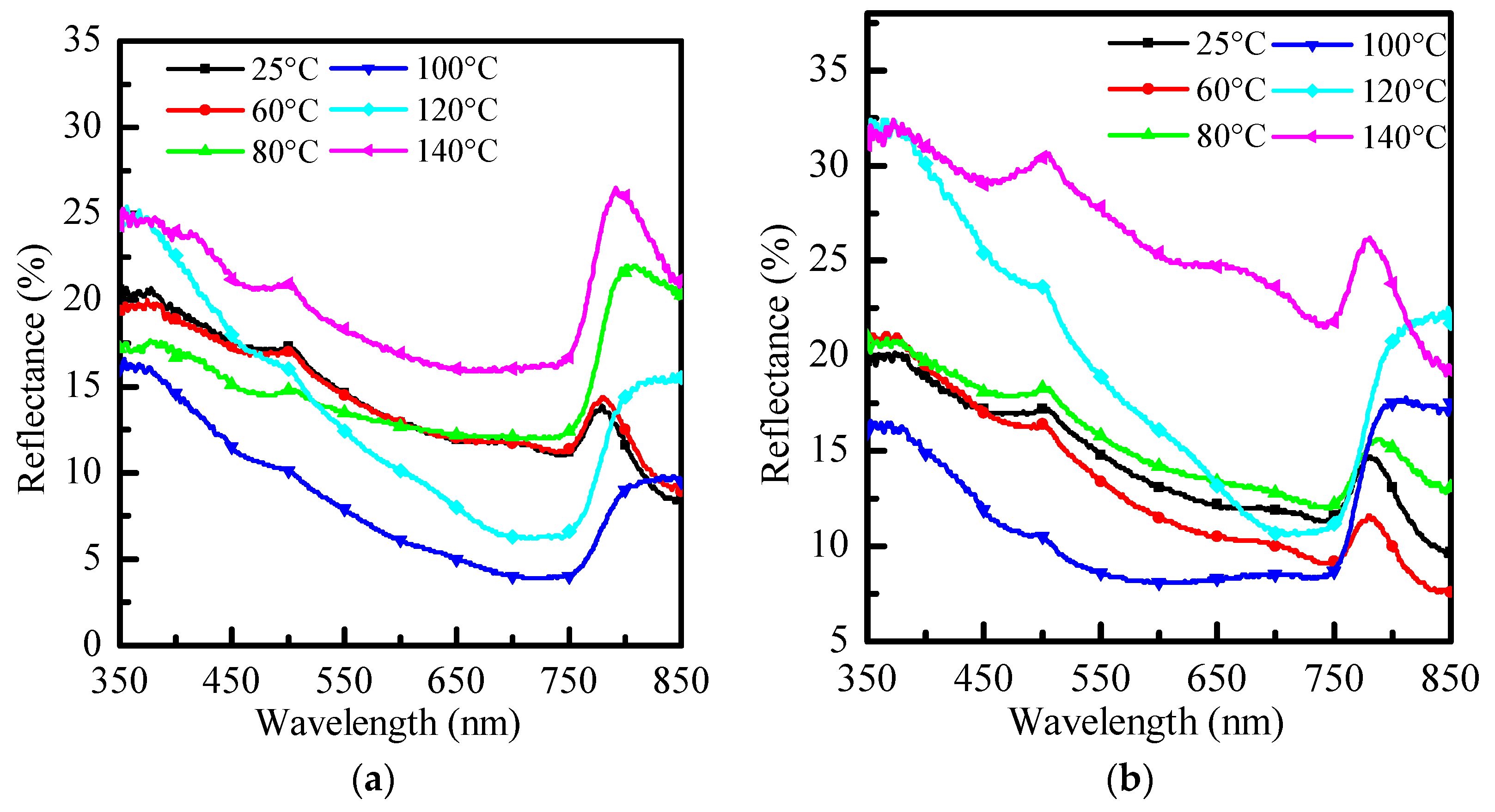
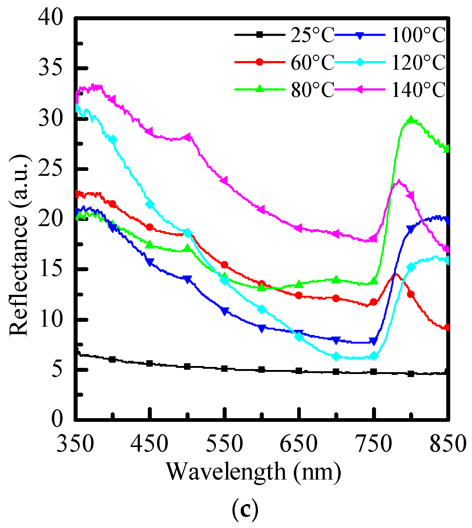
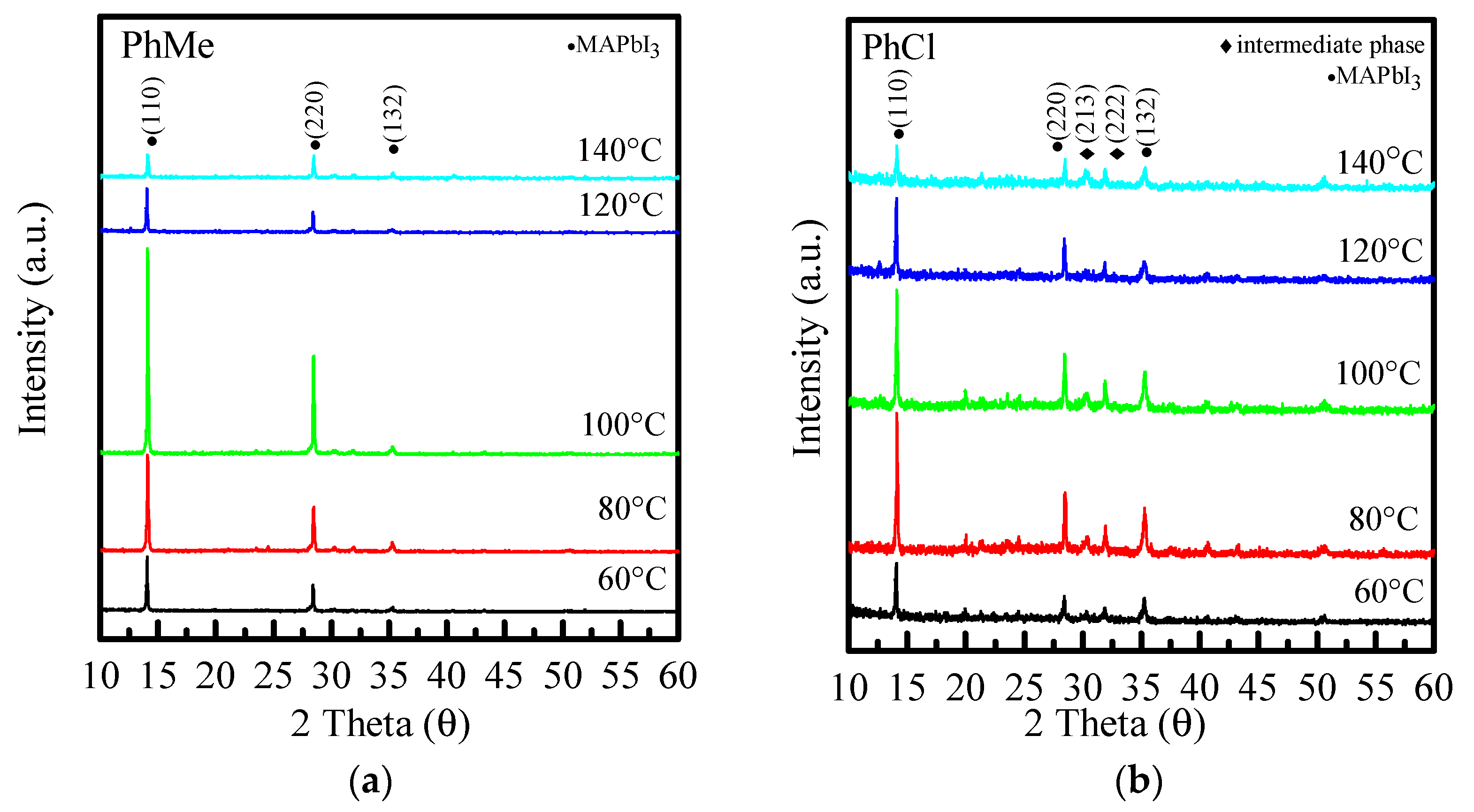
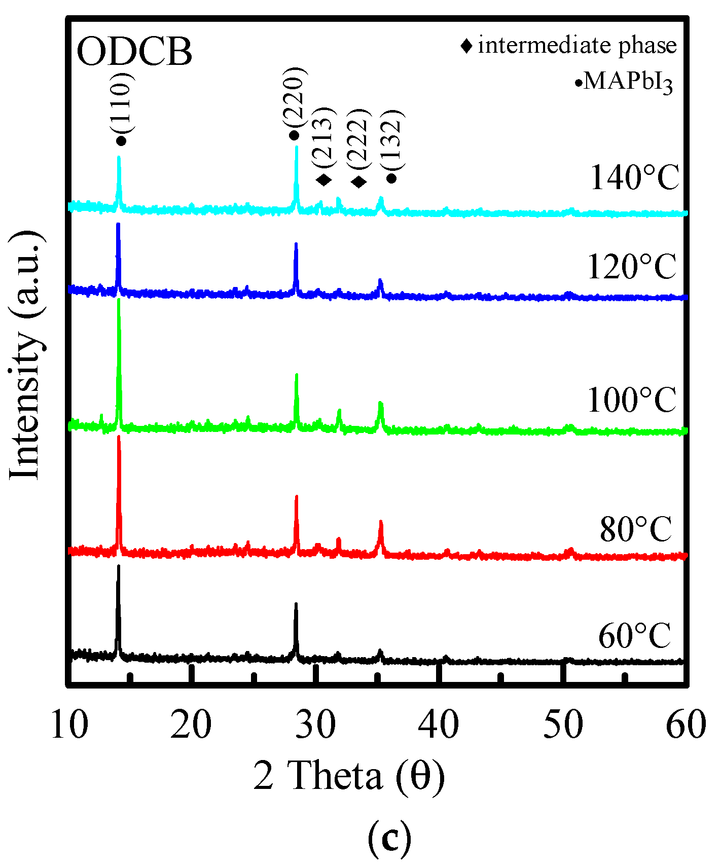
3. Results and Discussion

In this experiment, we analyzed different anti-solvents—toluene (PhMe), chlorobenzene (PhCl), and o-dichlorobenzene (ODCB) at room temperature (25 °C) and different re-annealing temperatures (60 °C, 80 °C, 100 °C, 120 °C, and 140 °C). Their effects on the optical properties and XRD diffraction pattern of MAPbI3 perovskite were be discussed, respectively. Figure 2 is a comparison of the absorbance optical properties of three different anti-solvents with no re-annealing at 25 °C and re-annealing at 60 °C~140 °C. Three of the images have typical material properties of MAPbI3, resulting in three images with obvious absorption peaks at 500 nm and 700 nm. After re-annealing, at short wavelengths, the absorbance decreases as the temperature rises, and the overall absorbance rises again when it reaches 80 °C. When it reaches 100 °C and 120 °C, the absorbance is also kept at a high level. The overall absorbance starts to decrease again when the temperature rises, as shown in Figure 2a. In Figure 2b, when re-annealing is carried out, the overall absorption increases to the best at 60 °C, and then starts to decline, reaching the lowest average absorption around 100 °C, and the initial absorption increases with increasing temperature, reaching 140 °C which will be similar to the absorption optimum at 60 °C. Finally, Figure 2c shows that without re-annealing, o-dichlorobenzene as an anti-solvent is not annealed, and absorbs very poorly in the 350 nm to 650 nm band. After re-annealing, the overall absorption was significantly improved, but with the other two anti-solvents, the change in absorption was small and did not change significantly due to the annealing temperature.
From this, it can be seen that using toluene as an anti-solvent has better absorption itself without re-annealing. However, compared with the other two anti-solvents, after annealing, the absorption stability of the sample at short wavelengths is poor. Using o-dichlorobenzene as an anti-solvent requires annealing to obtain sufficient absorption, but the absorption of the perovskite film is better than the other two anti-solvents at different re-annealing temperatures.
As shown in Figure 3a, in the 600 nm~700 nm band, the penetration changes significantly with temperature, with the strongest penetration at 100 °C. As shown in Figure 3b, there is a similar distribution to Figure 3a at long wavelengths. In Figure 3c, without re-annealing, there is an obvious strong penetrating power in the 350 nm~600 nm band, and it returns to the typical penetrating power distribution at long wavelengths. After re-annealing, the distribution returns to the typical distribution. 100 °C will have the strongest penetration at long wavelengths.
Figure 4 is a graph comparing the reflectance and optical properties of three different anti-solvents with no re-annealing at 25 °C and re-annealing at 60 °C~140 °C. As shown in the three figures, when re-annealing is performed, the overall reflection decreases as the temperature rises. When it reaches 100 °C, the lowest reflection occurs, and the overall reflection rises again when the temperature rises. When it reaches 120 °C, it will be close to no reflection. In the annealing temperature continue rises, the reflection rises higher and higher.
Figure 5 shows the XRD diffraction patterns of perovskites made from three different anti-solvents, re-annealed at 60 °C~140 °C. The crystalline phase is discussed next, and Figure 5a shows the XRD diffraction patterns at different annealing temperatures with toluene as the anti-solvent. It can be seen from Figure 5a that when the re-annealing temperature increases, the peak phase does not change much. Two strong peaks can be observed around 14° and 28°, which increase with the increase in the annealing temperature. The clean and strongest peak is at 100 °C, and then the peak begins to decrease with temperature. Figure 5b,c show that, similar to Figure 5b, when the re-annealing temperature increases, the peak phase does not change much. Compared with 30° and 32°, there are two more miscellaneous peaks, which are crystal phases (213) and (222), respectively. The peak is an intermediate product in the preparation of MAPbI3 [11], which means that the precursor solution in the preparation of the film is not completely converted into perovskite, which affects the absorption and even other performances of the film.
Finally, the team additionally calculated the grain size. Substitute the peak data into the Scherrer equation:
D = k λ B cos θ
The grain size (nm) of the three different anti-solvents at different re-annealing temperatures is obtained by calculation, as shown in Table 1. Where k is the Scherrer constant, if B is the half width of the diffraction peak, then k = 0.89, and if B is the integrated height and width of the diffraction peak, then k = 1, D is the crystal width (nm), θ is the Bragg diffraction angle in degrees, and λ is the X-ray wavelength corresponding to the copper target (1.54056 Å).
Since the grain size of perovskite is negatively correlated with the absorption, a larger grain size has fewer grain boundaries (grain boundaries are where electrons and holes recombine) and fewer grain boundaries reduces the crystal absorption. As the re-annealing temperature increases, there are larger grains, but when the re-annealing temperature reaches 120 °C, the thinned-out grains become smaller because the anti-solvent volatilizes too fast. The different boiling points and volatilization rates of the anti-solvents have different effects. In terms of grain size, chlorobenzene and o-dichlorobenzene with higher boiling points have the best re-annealing temperature around 120 °C, while toluene with lower boiling points has the best re-annealing temperature. The optimum re-annealing temperature is around 100 °C. As shown in Table 1, using toluene as the anti-solvent, at 80 °C, there is the smallest crystallite size; therefore, the lowest absorption and the best absorption are between 80 °C and 120 °C, consistent with the trend shown in Figure 2a.

4. Conclusions

In this study, toluene was used as the anti-solvent, without re-annealing, and it had the best absorbance. Compared with the other two anti-solvents, the obtained absorbance was also the best, but after re-annealing, perovskite had poor thermal stability. Using o-dichlorobenzene as an anti-solvent, it needs to be annealed enough to have sufficient absorbance and re-annealing. The thermal stability of perovskite is better than that of the other two anti-solvents at different re-annealing temperatures. The boiling point and volatilization rate of different anti-solvents affect the crystallization rate of perovskite, resulting in different grain sizes after crystallization and affecting the absorption of perovskite. Therefore, if one wants to improve the quality of perovskite films by annealing, anti-solvent plays a very important role. In this study, we compared three samples. The toluene used by most people is not the most ideal, instead the stability of o-dichlorobenzene after annealing makes it a better choice.

Author Contributions

Conceptualization, P.-Y.L., Y.-C.C., and Y.-H.W.; formal analysis, P.-Y.L., Y.-C.C., and Y.-H.W.; funding acquisition, P.-Y.L. and Y.-H.W.; investigation, P.-Y.L. and Y.-H.W.; resources, P.-Y.L. and Y.-C.C.; supervision, P.-Y.L. and Y.-H.W.; writing—original draft, P.-Y.L. All authors have read and agreed to the published version of the manuscript.

Funding

This work is sponsored by the Ministry of Science and Technology (MOST) of the Republic of China under contact number of 110-2221-E-390-019.

Institutional Review Board Statement

This study did not involve humans or animals.

Informed Consent Statement

This study did not involve humans.

Data Availability Statement

The data presented in this study are available on request from the corresponding author.

Conflicts of Interest

The authors declare no conflict of interest.

References

  1. Chen, Y.C.; Gao, C.Y.; Chen, K.L.; Huang, C.J. Surface plasmon-enhanced localized electric field in organic light-emitting diodes by incorporating silver nanoclusters. Appl. Surf. Sci. 2014, 295, 266–269. [Google Scholar] [CrossRef]
  2. Okamoto, Y.; Suzuki, Y. Mesoporous BaTiO3/TiO2 Double Layer for Electron Transport in Perovskite Solar Cells. J. Phys. Chem. C 2016, 120, 13995–14000. [Google Scholar] [CrossRef]
  3. Liu, D.; Kelly, T.L. Perovskite solar cells with a planar heterojunction structure prepared using room-temperature solution processing techniques. Nat. Photonics 2014, 8, 133–138. [Google Scholar] [CrossRef]
  4. Mahmud, M.A.; Elumalai, N.K. Low temperature processed ZnO thin film as electron transport layer for efficient perovskite solar cells. Sol. Energy Mater. Sol. Cells 2017, 159, 251–264. [Google Scholar] [CrossRef]
  5. Swarnkar, A.; Marshall, A.R.; Sanehira, E.M.; Chernomordik, B.D.; Moore, D.T.; Christians, J.A.; Chakrabarti, T.; Luther, J.M. Quantum dot–induced phase stabilization of a-CsPbI3 perovskite for high-efficiency photovoltaics. Science 2016, 354, 92–95. [Google Scholar] [CrossRef] [PubMed] [Green Version]
  6. Jacak, J.E.; Jacak, W.A. Routes for Metallization of Perovskite Solar Cells. Materials 2022, 15, 2254. [Google Scholar] [CrossRef]
  7. Wheeler, L.M.; Sanehira, E.M.; Marshall, A.R.; Schulz, P.; Suri, M.; Anderson, N.C.; Christians, J.A.; Nordlund, D.; Sokaras, D.; Kroll, T.; et al. Targeted Ligand Exchange Chemistry on Cesium Lead Halide Perovskite Quantum Dots for High-Efficiency Photovoltaics. J. Am. Chem. Soc. 2018, 140, 10504–10513. [Google Scholar] [CrossRef] [PubMed]
  8. Kim, H.S.; Lee, C.R.; Im, J.H.; Lee, K.B.; Moehl, T.; Marchioro, A.; Moon, S.J.; Humphry-Baker, R.; Yum, J.H.; Moser, J.E.; et al. Lead Iodide Perovskite Sensitized All-Solid-State Submicron Thin Film Mesoscopic Solar Cell with Efficiency Exceeding 9%. Sci. Rep. 2012, 2, 591. [Google Scholar] [CrossRef] [PubMed] [Green Version]
  9. Enustun, B.V.; Turkevich, J. Coagulation of Colloidal Gold. J. Am. Chem. Soc. 1963, 85, 3317–3328. [Google Scholar] [CrossRef]
  10. Reetz, M.T.; Helbig, W. Size-Selective Synthesis of Nanostructured Transition Metal Clusters. J. Am. Chem. Soc. 1994, 116, 7401–7402. [Google Scholar] [CrossRef]
  11. Huang, C.J.; Chen, K.L.; Chiu, P.H.; Sze, P.W.; Wang, Y.H. The Novel Formation of Barium Titanate Nanodendrites (BTNDs). J. Nanomater. 2014, 2014, 718918. [Google Scholar] [CrossRef]
  12. Guo, X.; McCleese, C.; Kolodziej, C.; Samia, A.C.; Zhao, Y.; Burda, C. Identification and characterization of the intermediate phase in hybrid organic–inorganic MAPbI3 perovskite. Dalton Trans. 2016, 45, 3806. [Google Scholar] [CrossRef] [PubMed]
  13. Chen, Q.; De Marco, N.; Yang, Y.M.; Song, T.B.; Chen, C.C.; Zhao, H.; Hong, Z.; Zhou, H.; Yang, Y. Under the spotlight: The organic–inorganic hybrid halide perovskite for optoelectronic applications. Nano Today 2015, 10, 355–396. [Google Scholar] [CrossRef] [Green Version]
  14. Song, T.B.; Chen, Q.; Zhou, H.; Jiang, C.; Wang, H.H.; Yang, Y.M.; Liu, Y.; You, J.; Yang, Y. Perovskite solar cells: Film formation and properties. J. Mater. Chem. A 2015, 3, 9032–9050. [Google Scholar] [CrossRef]
  15. Zhou, D.; Zhou, T.; Tian, Y.; Zhu, X.; Tu, Y. Perovskite-based solar cells: Materials, methods, and future perspectives. J. Nanomater. 2018, 2018, 8148072. [Google Scholar] [CrossRef]
  16. Wang, H.; Kim, D.H. Perovskite-based photodetectors: Materials and devices. Chem. Soc. Rev. 2017, 46, 5204–5236. [Google Scholar] [CrossRef] [PubMed]
  17. Zheng, C.; Rubel, O. Unraveling the water degradation mechanism of CH3NH3PbI3. J. Phys. Chem. C 2019, 123, 19385–19394. [Google Scholar] [CrossRef] [Green Version]
  18. Chi, W.; Banerjee, S.K. Achieving Resistance against Moisture and Oxygen for Perovskite Solar Cells with High Efficiency and Stability. Chem. Mater. 2021, 33, 4269–4303. [Google Scholar] [CrossRef]
  19. Li, M.; Zhang, Y.; Tang, X.; Li, J.; Wang, S.; Li, T.; Zhao, H.; Li, Q.; Wang, Q.; Yao, J. Improving performance of hybrid perovskite/graphene-based photodetector via hot carriers injection. J. Alloys Compd. 2022, 895, 162496. [Google Scholar] [CrossRef]
  20. Deng, X.; Cao, Z.; Li, C.; Wang, S.; Hao, F. Benzotriazole derivative inhibits nonradiative recombination and improves the UV-stability of inverted MAPbI3 perovskite solar cells. J. Energy Chem. 2022, 65, 592–599. [Google Scholar] [CrossRef]
  21. Lien, S.Y.; Liu, S.Y.; Chen, W.R.; Liu, C.H.; Sze, P.W.; Wang, N.F.; Huang, C.J. The Influence of Argon Plasma on Organic Perovskite MAPbI3 Film Doped with Inorganic Perovskite CsPbI3 Quantum Dots (QDs). Crystals 2022, 12, 799. [Google Scholar] [CrossRef]
  22. Laska, M.; Krzemińska, Z.; Kluczyk-Korch, K.; Schaadt, D.; Popko, E.; Jacak, W.A.; Jacak, J.E. Metallization of solar cells, exciton channel of plasmon photovoltaic effect in perovskite cells. Nano Energy 2020, 75, 104751. [Google Scholar] [CrossRef]
Figure 1. Schematic diagram of fabrication of perovskite and thin film.
Crystals 12 01074 g001
Figure 2. Absorption spectra of (a) toluene (PhMe), (b) chlorobenzene (PhCl), and (c) o-dichlorobenzene (ODCB) at different annealing temperatures, respectively.
Crystals 12 01074 g002aCrystals 12 01074 g002b
Figure 3. Transmittance graphs of (a) PhMe, (b) PhCl, and (c) ODCB at different re-annealing temperatures, respectively.
Crystals 12 01074 g003aCrystals 12 01074 g003b
Figure 4. Reflectance graphs of (a) PhMe, (b) PhCl, and (c) ODCB at different re-annealing temperatures, respectively.
Crystals 12 01074 g004aCrystals 12 01074 g004b
Figure 5. XRD diffraction patterns of (a) PhMe, (b) PhCl, and (c) ODCB at different re-annealing temperatures, respectively.
Crystals 12 01074 g005aCrystals 12 01074 g005b
Table 1. Grain sizes produced by different anti-solvents and annealing temperatures.
Toluene (nm)Chlorobenzene (nm)o-Dichlorobenzene (nm)
60 °C55.8243.7650.79
80 °C50.5851.9452.13
100 °C59.9548.0154.79
120 °C57.1556.0957.07
140 °C55.5848.8454.05
Anti-solvent boiling point110 °C131 °C180 °C
Publisher’s Note: MDPI stays neutral with regard to jurisdictional claims in published maps and institutional affiliations.

