1. Introduction
Miniature metallic parts and products for medical applications are inevitably formed by metal forming in dry, especially by cold, forging [
1]. Other metals and metallic alloys than the austenitic stainless steels, pure titanium and titanium alloys are never allowed to be utilized as a matrix of medical and biomedical things. The expecting metal-forming tools must have a capacity to shape these stainless steel, pure titanium and titanium alloy works without significant friction and wear and with geometric accuracy necessary for medical usage [
2]. However, these work materials are difficult to make metal forming accurate. This dry, cold forging cannot be put into practice without surface treatment or die material selection to lower the tool damage and to improve the product quality [
3]. The ceramic coatings such as TiN, TiCN, CrN, TiSiN and so forth have the potential to be used for dry forging of stainless steels and titanium. Friction and wear by high stress transients in continuous dry forging processes become the first issue to shorten the ceramic-coated tool life [
4]. A higher friction coefficient than 0.3 was experienced in the ball-on-disc testing of those ceramic coatings against the stainless steel and titanium balls. By using the DLC (diamond-like carbon) coating as their top coating layer, this problem is solved; as stated in [
5], the low friction and wear state were preserved in dry for a long running distance.
The second issue in this dry, cold forging is galling or severe adhesion on the contact interface between those coatings and the fresh surfaces of stainless steels and titanium works during the forging process. As reported in [
6], a significantly low formability by using the SKD11 dies was never improved in the deep-drawing test of titanium sheets, even by using Al
2O
3, Si
3N
4, ZrO
2 and SiC-sintered dies. Almost all the ceramic coatings, including the DLC coating, suffered from a severe adhesion of titanium, as well as metal-sticking, to decelerate the tool life [
7]. In addition to this problem, titanium oxide debris particles splash from the titanium work, adhere to the die-work contact interface and hinder the continuous forging operations [
8].
In previous studies [
9,
10], this galling behavior on the pure titanium work onto the die surface was reconsidered by die material selection. Thick SiC coating was employed instead of the sintered SiC die for the dry stamping of titanium works. Although the sintered SiC had porosity and glassy zones, the synthesized SiC coating by the thermal CVD (chemical vapor deposition) had a dense β-phase and 3C-SiC structure [
10,
11]. On the other hand, SiC coatings by PVD (physical vapor deposition) or other CVD processes were amorphous, with much lower density than 3C-structured SiC coating. The CNC (computer numerical control)-stamping system was utilized in [
11,
12] to experimentally demonstrate that a thick β-SiC coating could work as a die for dry, cold microforging. SEM (scanning electron microscopy)-EDX (electron-dispersive X-ray spectroscopy) analysis on the contact interface of this SiC coating in [
12] revealed that a galling-free condition could be sustained up to a higher reduction than 30%. In the literature, the galling phenomena of titanium onto the die surface were discussed on the material compatibility on the contact interface between the die and work [
13,
14,
15]. After the classical theory by the HSAB (Hard and Soft Acids and Base) principle [
6,
13,
14], titanium ions belonging to the hard acid group were thought to react on the contact interface with silicon-oriented ions in the hard base group. After computational surface chemistry [
15], titanium had less of a possibility of change in the DOS (Degree of State) of electrons from its metallic bonding to covalent one in the SiC. In addition to the above chemical explanation on the galling behavior, the mechanical interaction between the SiC coating and titanium must be taken into account after [
16].
In the present paper, a thick β-SiC coating die system was prepared for a dry, cold forging test to investigate the material compatibility of AISI316L stainless steel and TP328H titanium to SiC coating, even in a higher reduction of the thickness in forging. Both wires with a diameter of 1 mm were successfully shaped into flat, pentagonal prism bars without adhesion of the metallic work materials to SiC coating surfaces. No significant differences were noted in the in situ measured power–stroke relationship during the cold forging of both works. Precise SEM-EDX analyses on the contact interface between the SiC coating and the forged works up to the reduction of 35% revealed that thin oxide debris deposits were formed on the contact interface. The iron-chromium-nickel oxide film was formed after cold forging the AISI316L wires, and a titanium oxide film was also formed after forging the TP328H titanium wires. In particular, the contact interface of SiC coating to titanium wire was uniformly covered by thin metallic oxide films. The isolated carbon was only detected at the center of the contact interface between the SiC coating and titanium wire, together with the titanium oxide film. This difference in the chemical response of the SiC coating during forging revealed the importance of material compatibility to sustain the galling-free forging process in dry.
2. Experimental Procedure
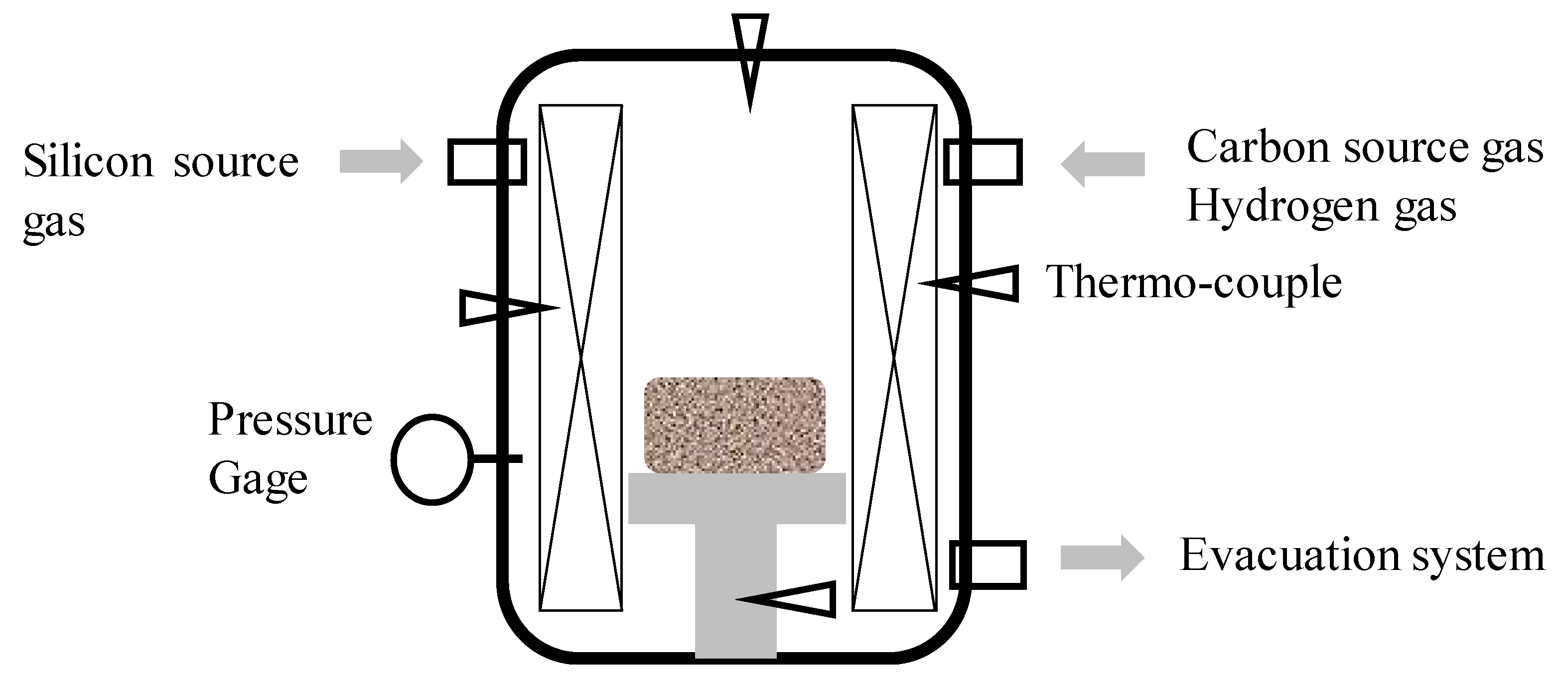
Thermal CVD processing was used to deposit a thick SiC coating onto the sintered SiC die substrates.
Figure 1 illustrates this CVD coating system, together with the evacuation and gas supply systems. The silicon- and carbon-source gasses, as well as pure hydrogen gas, were introduced into the chamber up to the pressure of 10 kPa, significantly higher than the conventional PVD and CVD coaters. In the following experiments, silicon-chloride gas with the flow rate of 600 mL/min was utilized for thermal CVD process. Its duration time was 28.8 ks for 8 h.
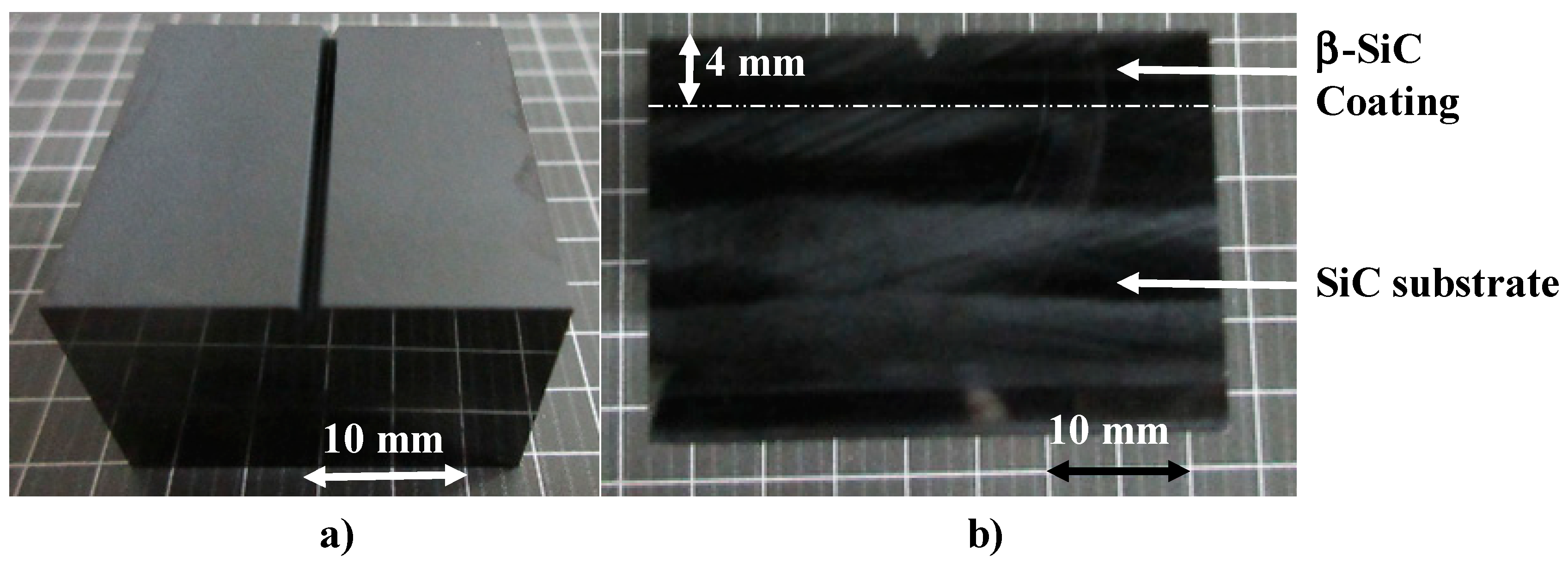
A sintered SiC block with the relative density of 99.5 % was prepared as a substrate for this thermal CVD process and polished to have the average roughness less than 0.1 μm before coating. The holding temperature was controlled to be constant by 1500 K. After cooling in the chamber, the CVD-coated SiC block was directly cut by the diamond saw and polished by chemical buffing to shape the SiC-coated SiC cubic punch and die. SiC coating thickness was 4 mm. As-buffed SiC-coated SiC substrate was straightforwardly used as a punch; e.g., its size was 24.6 mm × 24.6 mm × 25 mm. Fine diamond sawing was further utilized to form the triangular cavity into the SiC-coated SiC die with the size of 26.5 mm × 26.5 mm × 18.5 mm. The cross-section of this cavity was an isosceles triangle with a depth of 0.45 mm and an inlet width of 2 mm.
Figure 2 depicts a SiC-coated SiC core die for dry, cold forging.
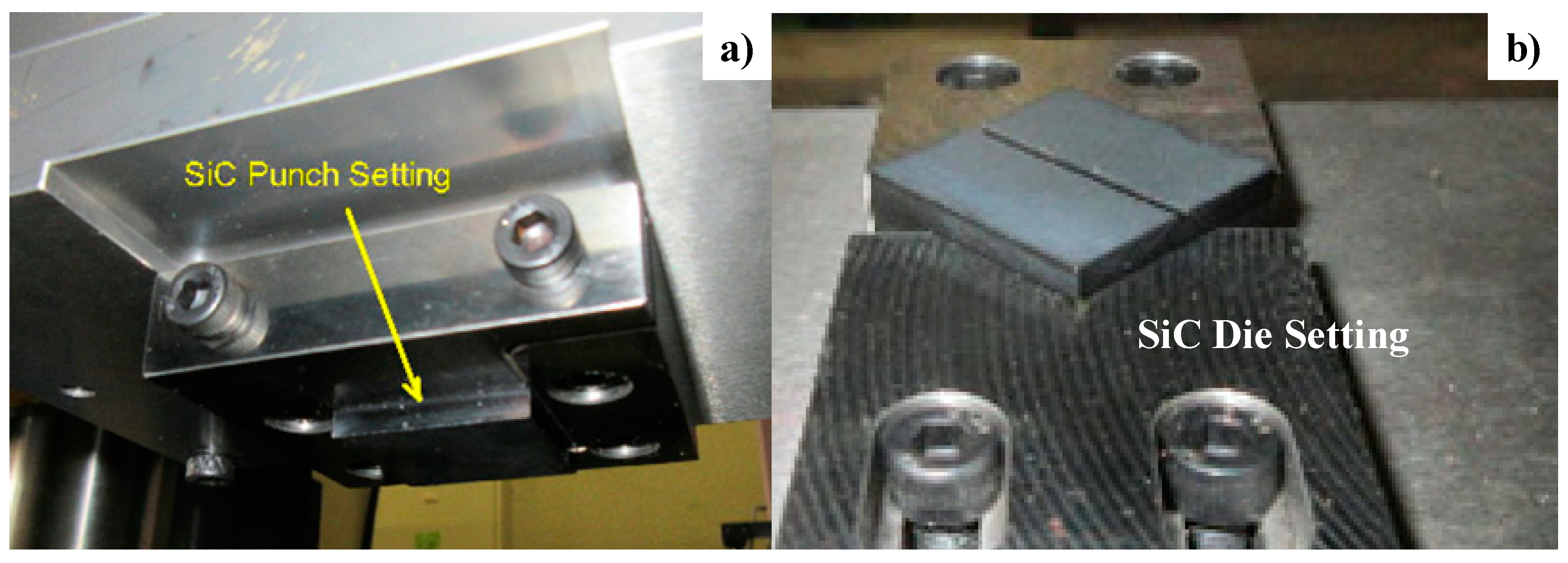
These SiC punch and die were fixed into the upper and lower cassette dies, as depicted in
Figure 3a,b, respectively. These cassette-die sets were locked at the upper and lower bolsters of the CNC stamping system. This stamper had four servomotors with independent controllability to move upward and downward in the programmed loading sequence. Owing to this controllable adjustment among four loading axes, the following stamping is free from eccentricity in loading and unloading. The maximum load was 50 kN; the loading sequence was controlled by the time history of the stroke. In the following forging process, the punch was controlled to move down from the original height of 80 mm down to 42 mm by 10 mm/s for 3.8 s in the first term. In the second term, the stroke speed was reduced to 0.02 mm/s to precisely decrease the height of 42.0 mm to 41.7 mm for 15 s. At this height, the SiC punch was just in contact with the work during this term. In the third term, the work was forged to the specified height (H
g) for each reduction of diameter (r); e.g., H
g = 41.5 mm at r = 10%, H
g = 41.4 mm at r = 20% and H
g = 41.1 mm at r = 35%, respectively. In the fourth term, the stroke was constant by H = H
g for each reduction for 0.5 s before increasing the stroke by 10 mm/s up to the original position. In the following successive forging operations by ten times, the above stamping operation was repeated by 10 times for each work with the use of same die system.
Two wire specimens with the diameter of 1.0 mm and the length of 20 mm were employed as a work in the following forging experiment: austenitic stainless steel-type AISI316L wire and pure titanium-type TP328H wire in industrial grade II. The former chemical compositions are listed as follows: carbon content was 0.02%, silicon 0.52%, manganese 0.84%, phosphor 0.027%, sulfur 0.001%, nickel 12%, chromium 17%, molybdenum 2% and iron for balance. The latter consists of hydrogen by 0.0012 mass%, oxygen 0.097 mass%, nitrogen 0.007 mass%, iron 0.042 mass%, carbon 0.007 mass% and titanium for balance.
3. Experimental Results
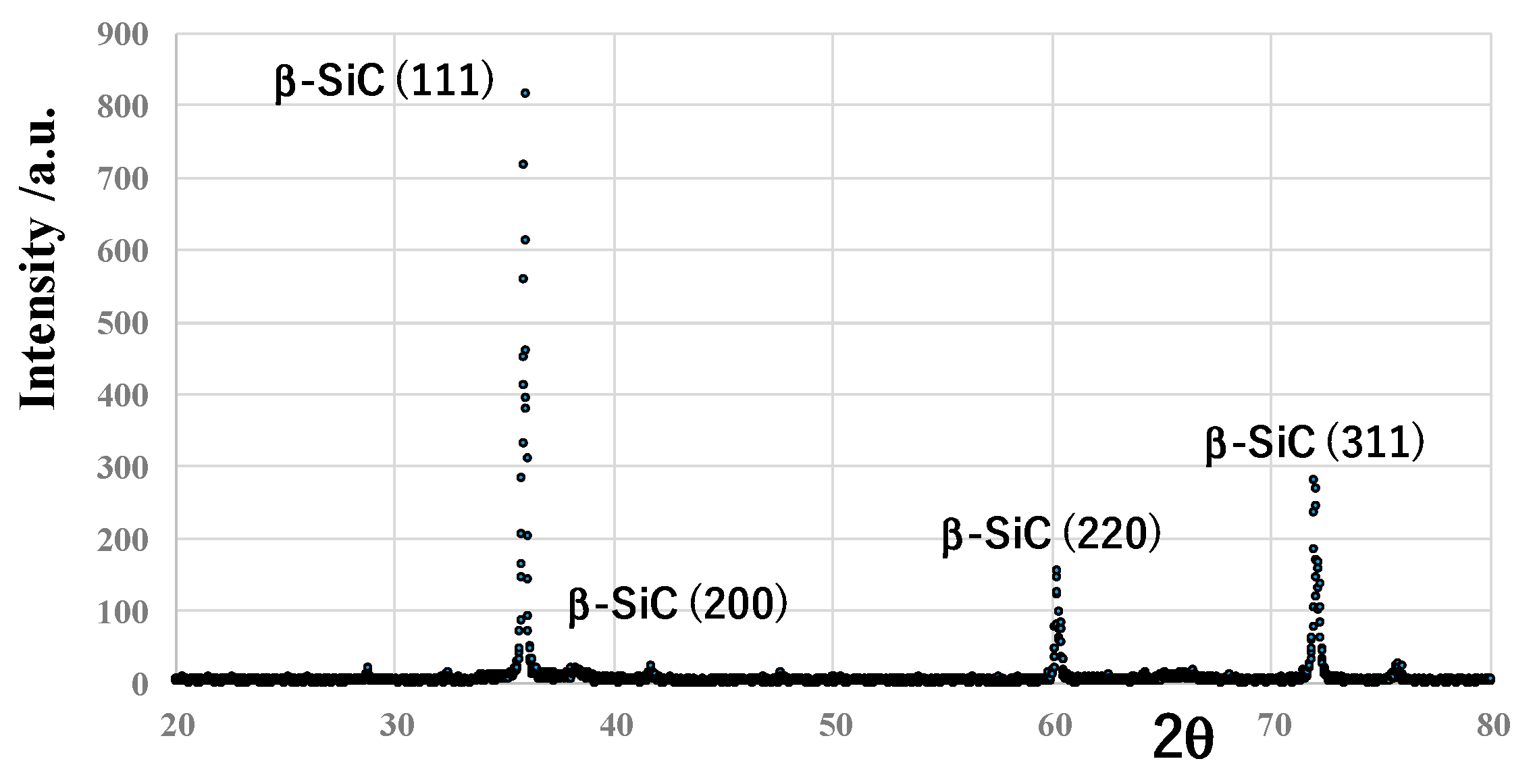
The CVD-coated SiC layer is characterized by XRD (X-Ray diffraction; SmartLab, Regaku, Tokyo, Japan), with the monochromatic CuKα radiation (λ = 0.1542 nm) and Bragg–Brentano geometry (40 kV, 30 mA) as well as SEM (SU-70, Hitachi, Tokyo, Japan). SEM-EDX analysis is used to explain the material compatibility on the contact interface between the AISI316L/TP328H wires and SiC coating.
3.1. Characterization on the SiC-Coated SiC
The CVD-coated SiC layer on the sintered SiC substrate with the thickness of 4 mm has a single phase of β-SiC and 3C-SiC crystallographic structure, as shown in
Figure 4. In measurements, 2θ ranged from 20° to 80°, with the scanning speed of 5 mm/min and the step angle of 0.02°. Different from other PVD and CVD-coated SiC films, the amorphous phase with broad peaks was not detected by XRD analysis.
SEM image on this β-SiC coating is shown in
Figure 5. The average grain size (D
grain) was measured from this SEM image after chemical etching; D
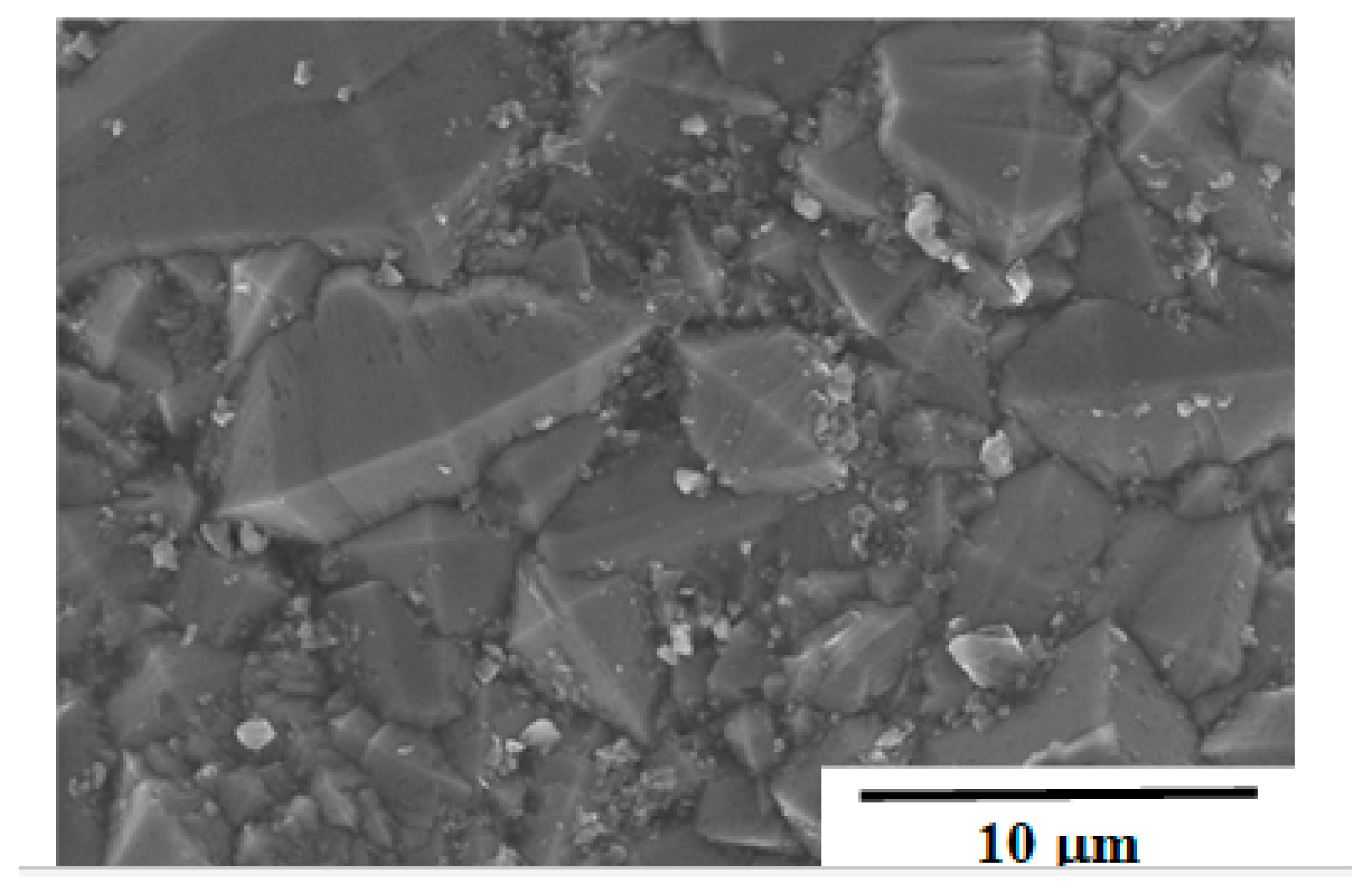
grain = 10 μm and free from extraordinary grain growth. This homogeneity in the microstructure is controllable by the present CVD process conditions.
3.2. Dry, Cold Forging Testing of the AISI316L Wire
The AISI316L wire with the diameter of 1.00 mm was cold-forged to a flat, pentagonal prism bar.
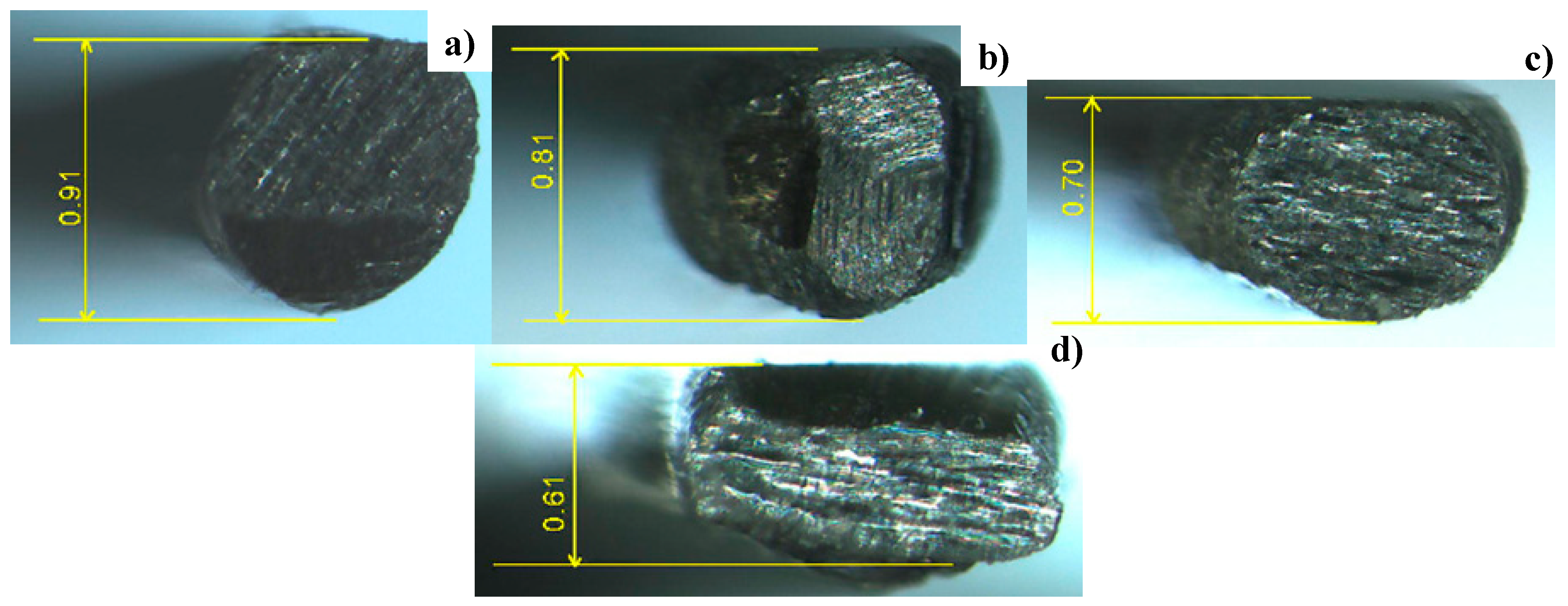
Figure 6 depicts the variation of the cross-section for the forged AISI316L wires with increasing the reduction (r) of the diameter. The lower part of the wire flows elastoplastically into a triangular prism cavity of SiC coating core die, while its upper part is compressed to extend along the contact interface on the SiC coating punch. When r > 20%, the main plastic flow of the wire advances in the lateral direction on the SiC coating punch head, together with filling into a triangular cavity of core die. Hence, the contact interface area monotonously extends in the lateral direction with increasing r under high compressive pressure.
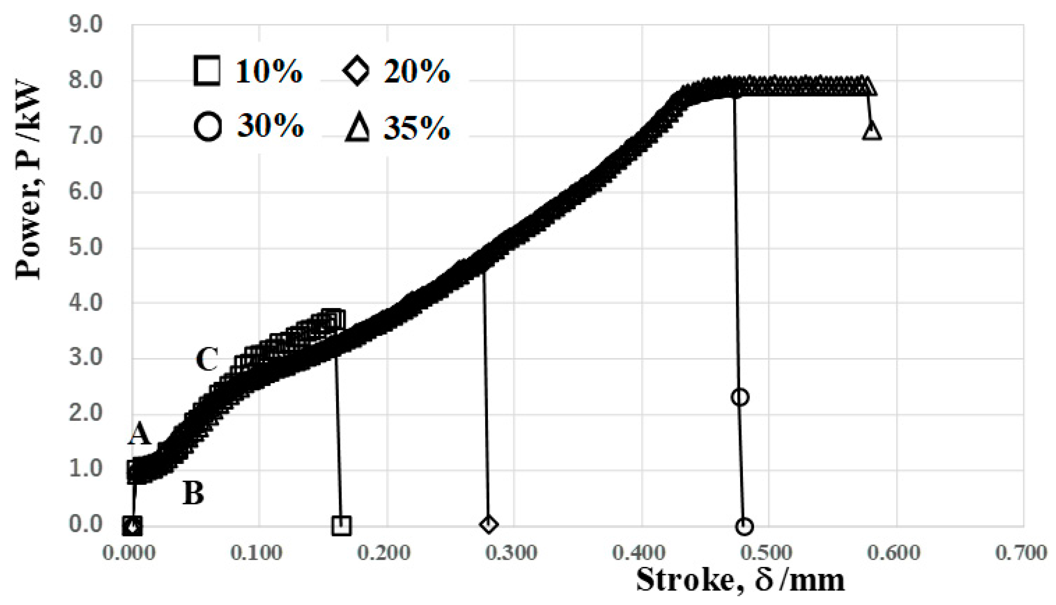
As stated in the above, the programed loading sequence in this CNC stamper is independently driven by four motors; the total power, as well as the stroke, are in situ monitored in the present forging experiment.
Figure 7 depicts the relationship between the applied power and stroke in forging down the reduction by 10%, 20%, 30% and 35%, respectively. At point A, the punch commences to touch the wire surface; then, the wire is compressed in the axial direction up to point B. The flattening process of the wire head advances from this point. In the following reduction of the diameter, the contact interface area between the SiC coating punch and wire expands monotonously with increasing the reduction of the diameter. At point C, the lower part of the wire starts to fill into a cavity on the die. After this point, the work hardening of the AISI316 wires takes place together with flattening along the SiC coating punch head and filling into a die cavity until the applied power reaches a maximum of 8 kW.
3.3. Dry, Cold Forging Testing of the TP328H Pure Titanium Wire
The TP328H wire with a diameter of 0.98 mm was employed as a work material for dry, cold forging experiments under the same setup as was used in forging the AISI316L wire to investigate the effect of the work material flow on the forging behavior, as well as the surface condition on the contact interface.
Figure 8 depicts the variation of the cross-section of forged titanium wires up to r = 10%, 20% and 35%, respectively. When r = 35%, the flattening width at the wire head becomes broader than 1 mm; its filling depth into the triangular cavity reaches 0.3 mm. The pure titanium wire is shaped into a flat pentagonal bar in the similar manner to the cold forging of the AISI316 wire.
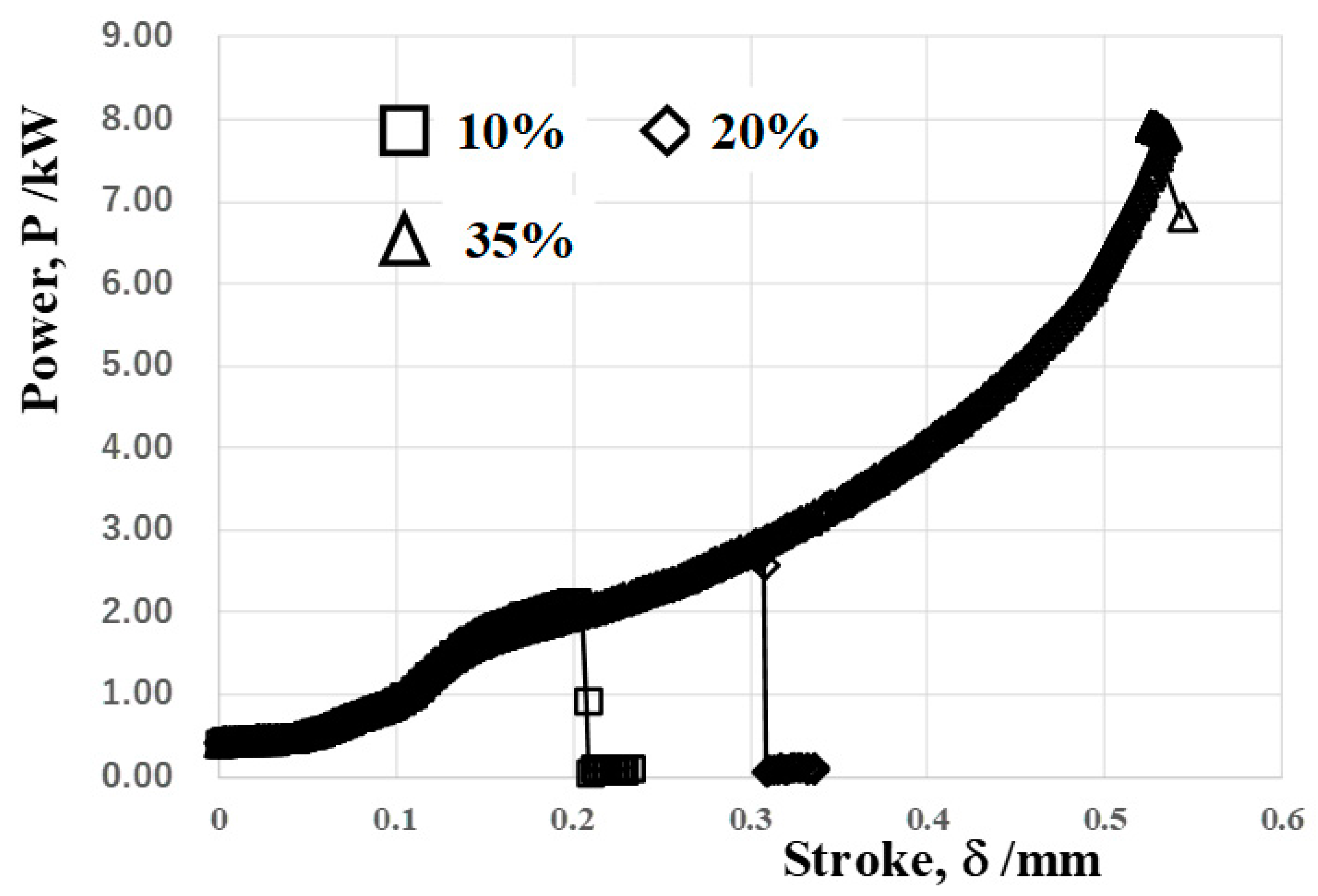
Figure 9 shows the applied power to the stroke relationship in the cold forging of the TP328H wire. This relationship is similar to
Figure 7; the dry, cold forging behavior of the TP328H wire is nearly the same as that of the AISI316L wire. At the same applied power in
Figure 7 and
Figure 9, more stroke advances in the forging of the TP328H wire are, e.g., at P = 5 kW, d = 0.45 mm for TP328H and d = 0.28 mm for AISI316L. This implies that work hardening is more enhanced by the flattening process of the AISI316L wire than the TP328H one. Even when applying the maximum power of 8 kW in the stamping system, the highest reduction of the diameter is also limited by 35% in the cold forging of the TP328H wire.
3.4. SEM-EDX Analysis on the Contact Interface of the Punch to the Work Materials
The contact interface between the fresh surface of the works and the SiC coating punch head is mechanically subjected to high compressive stress in the normal direction and to shear straining in the lateral direction during dry, cold forging. The punch head surface is also subjected to the chemical attack of a fresh work metal during the shearing process under high pressure. In particular, when forging the work materials continuously, either a metallic part of the fresh surface could adhere onto the contact interface as a debris fragment or a part of the work surface oxide layer and oxidized fresh surface could be splashed onto the interface. The severity of the galling is dependent on the chemical activeness of the work materials, as well as the mechanical transients in the work hardening on the contact interface. Both the AISI316L and TP328H wires were continuously forged by 10 shots up to r = 35% under the same experimental setup. Each SiC coating punch after the dry forging experiment is prepared for SEM-EDX analysis to describe the above galling behavior on the contact interface.
Figure 10a depicts the optical microscopic image on the SiC coting punch head surface. A thin trace is left on it after continuously forging the AISI316L wire. High-resolution SEM analysis and element mapping by EDX are performed at the center of this trace, as shown in
Figure 10b. This region corresponds to the initial contact interface of the AISI316L wire at r < 10%, where high normal stress is applied to the SiC coating.
Figure 10c depicts the element mapping of carbon, silicon, oxygen, iron, chromium and nickel on this initial contact interface. Since the mapping among Fe, Cr, Ni and O is coincident with each other, Fe-Cr-Ni oxide fragments deposit on the SiC coating surface. Carbon and silicon distribute uniformly on the surface, except for these oxide fragments; in particular, no concentration of carbon is detected on the contact interface. The SEM analysis in
Figure 10d proves that thin Fe-Cr-Ni oxide fragments deposit irregularly on the SiC coating head surface during these continuous cold forging processes by ten shots.
When forging the TP328H wire successively 10 times with the use of the SiC-coated SiC punch and die, a trace was also left on the surface of the SiC coating in a similar manner to
Figure 10, as shown in
Figure 11a.
Figure 11b depicts that this trace consists of two zones, e.g., the black zone at its center and the white zones neighboring to this black one. At first, while this zone is analyzed by SEM-EDX, element mapping by carbon, silicon, oxygen and titanium is shown in
Figure 11c. Although both the carbon and silicon sparsely distribute at the layers with high contents of titanium and oxygen, C and Si are uniformly present on the white zone. This implies that titanium oxide layers are formed in the radial direction from the center of the contact interface on the SiC coating surface, as shown in
Figure 11d. This linear assembly of titanium oxide layers look white in
Figure 11a,b. Comparing
Figure 10 and
Figure 11, Fe-Cr-Ni oxide debris fragments agglomerate in the network by a combination of each oxide debris fragment on the SiC coating. On the other hand, titanium oxide debris formed the thin layers in the radial direction from the center of the contact zone with the flattening of the TP328H wire by a reduction of its diameter. A three-dimensional profile of the debris layer was measured by optical profilometer (Keyence) to find that the layer thickness was less than 1 μm.
In seconds, the black zone at the center of contact trace was analyzed by SEM-EDX in a similar manner to
Figure 10 and
Figure 11. As shown in
Figure 11a,b and
Figure 12a,b, SEM-EDX analysis was made on the black zone of the same contact trace, which corresponded to the first contact interface of the SiC coating punch to the TP328H wire. Element mapping on the carbon, silicon, oxygen and titanium at the center of the trace is shown in
Figure 12c. The titanium and oxygen mappings coincided with each other, the titanium oxide debris particles deposited in a layer on the SiC coating. These titanium oxide debris deposit layers were also formed radially from the center of the black zone in a similar manner to
Figure 11c. A little significant difference in the titanium oxide layer deposition was seen between
Figure 11 and
Figure 12 or between the white and black zones in the contact interface.
Different from the uniform carbon mapping in
Figure 11c, the carbon agglomerates were found on the uncovered SiC surface between the titanium oxide debris clusters. This implies that the black dots at the center of the trace in
Figure 11b and
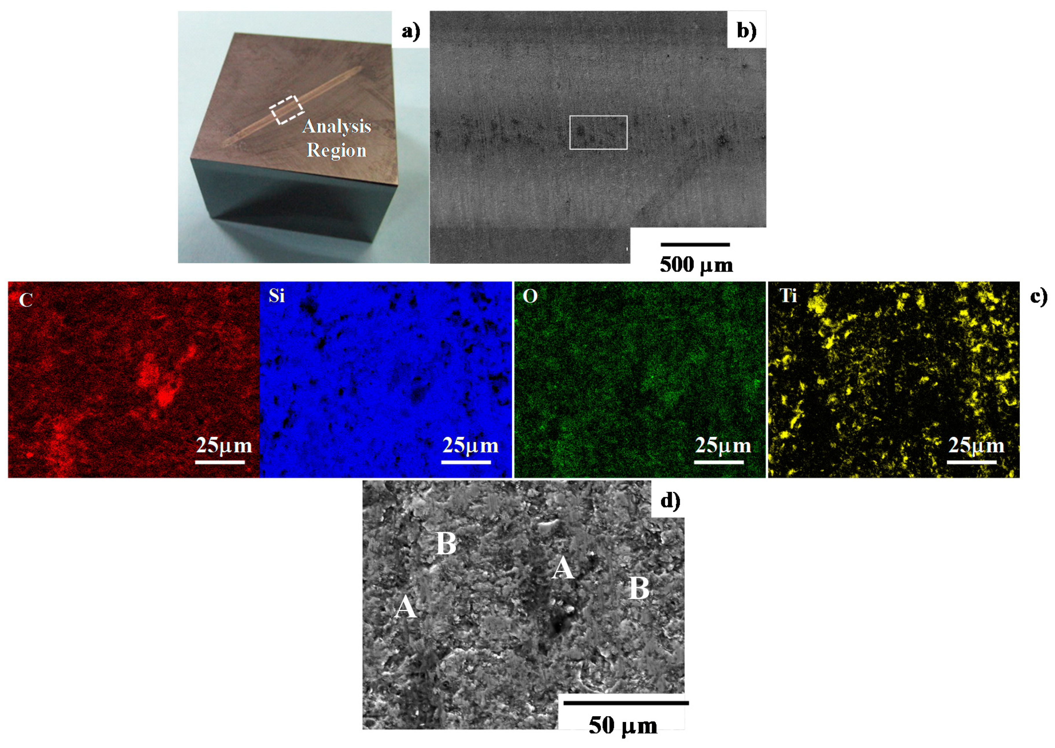
Figure 12b are carbon agglomerates. There was no carbon source in the TP328H wire other than SiC to leave the carbon trace on the contact interface. No carbon agglomerate was detected in other interface areas, except for the center of the interface. This implies that carbon could isolate from the SiC coating and form an agglomerate in the initial contact zone to pure titanium. The SEM analysis in
Figure 12d revealed that isolated carbon agglomerates were formed together with titanium oxide debris thin films on the contact interface between the SiC coating and TP328H wire during dry, cold forging in continuous.
4. Discussion
No significant adhesion of the work materials by metallic mass transfer was detected on the contact interface of the SiC coating punch and die of both the AISI316L and TP328H wires, even after continuous forging up to the reduction of 35% by ten shots. This proves that β-SiC coating with the 3C structure is an effective die material for galling-free, dry, cold forging with a high reduction of thickness. When forging the AISI316L wire, its oxide debris fragments splashed and deposited onto the SiC coating surface. These oxide deposits were shaped irregular not to form a thin film on the SiC coating punch surface. On the other hand, titanium oxide debris particles also splashed and deposited onto the SiC coating and formed a thin layer in the radial direction from the center of the contact surface when forging the TP328H wire. This implies that Fe-Cr-Ni oxide debris deposits have nothing to do with the plastic flow of the AISI316L wire in the flattening along the contact interface but that the titanium oxide debris film grows and extends by itself with the flattening of the TP328H wire during dry forging. A little contact trace was detected on the triangular cavity surfaces of the core die. The fresh forged surfaces of the AISI316L and TP328H wires were flat and smooth, without traces of adhesion.
The above difference in the oxide debris deposition comes from the material characteristics of metallic oxides. As was discussed in [
17], the oxide fragments of stainless steels were easy to deposit onto the tool surface in hot processing, and their stacking had a risk to cause metallic sticking on the contact interface. On the other hand, titanium lubricious oxide formed a deformable thin film on the tool surface to reduce the friction and wear [
18]. This difference of metallic oxide layers in mechanical properties reflects on the debris particle deposition behavior onto the contact interface between the metallic wire and SiC coating.
Another difference detected on the contact interface between the AISI316L/titanium works and SiC coating is a carbon agglomeration in dots with the size of 10 to 20 μm at the center of the interface. There are two mechanisms to trigger this carbon isolation from 3C-structured, β-phase SiC coating [
11,
12]. In the processing of single-crystalline SiC, carbon is left by an isolation of Si on the SiC surface and grows as a graphene layer at elevated temperatures over 1500 K [
19]. In the present situation, the flash temperature on the contact interface between the TP328H wire and SiC coating was much lower than the critical temperature to ignite Si isolation from the SiC crystals. In the phase diagram for the Si–C binary system [
20], the β-SiC crystalline structure was stable in the higher carbon content regions than 50% from room temperature (RT) and an atmospheric pressure up to 2400 K and 50 GPa, respectively. Assuming that titanium wire is elastoplastically in contact on the SiC coating, with an initial contact area of 10 μm × 20 mm by the load of 10 kN in
Figure 9, the applied pressure on the contact surface reached to 5 GPa at most. Hence, the Si–C phase diagram teaches that an unstable isolation of carbon from the β-SiC phase could be never feasible at this low pressure and low flash temperature range.
The processing condition has an influence on this carbon isolation with the aid of the chemical activeness of titanium to SiC. A similarity of the power to the stroke relationship in forging the AISI316L and T328H wires proves that both wires deform elastoplastically to pentagonal bars under nearly the same stress transients. In this transient, the applied stress becomes the maximum when the work contacts the SiC coating. Under this mechanical condition, carbon is forced to isolate from the SiC coating only at the initial contact area to titanium, not to stainless steel. After [
21], carbon in the 6H-structured SiC is isolated from the coating and reacted with titanium at the elevated temperature. This suggests that the chemical compatibility of carbon to the fresh titanium of forged wire under a highly stressed contact interface could drive this carbon isolation from a β-SiC layer at RT and that isolated carbon could agglomerate only at the initial contact zone between the TP328H wire and SiC coating, even in dry, cold forging, without any detection of TiC and SiC debris. Through further analyses by Raman spectroscopy, this formation mechanism of free carbon agglomerates can be explained in detail.
Dry, cold forging with a high reduction is the first step in the manufacturing of austenitic stainless steel and titanium biomedical parts and tools. Corresponding to no adhesion of metal transfers, as well as the formation of thin oxide debris agglomerates and films onto the SiC coatings, the forged wire surface becomes smooth and flat enough to advance to the next step in the near net shaping of the medical parts and tools. In particular, dry, cold forging with a high reduction of thickness, as well as the following near-net shaping, are essential to fabricate the titanium miniature biomedical parts and operation tools, as pointed out in [
1,
2]. The present approach provides a cost-competitive production line to shape these products from raw stainless steel and titanium bars and wires.
5. Conclusions
A thick SiC coating with a β-phase and 3C structure has chemical inertness enough to suppress the metallic adhesion with a mass transfer from the fresh surface of flattening work materials during dry, cold forging. When forging the AISI316L wire, iron-chromium-nickel oxide debris fragments deposit onto the contact interface to the SiC coating. These irregular oxide deposits never stuck on the SiC coating surface to hinder the flattening process in dry, cold forging. On the other hand, when forging the TP328H wire, titanium deformable oxide debris particles deposited regularly in the radial direction from the center of the contact interface and formed a thin layer. In addition, carbon isolates from the SiC 3C structure and agglomerates were only at the initial contact interface.
Galling-free, dry, cold forging with a higher reduction of thickness than 30% proves that the SiC-coated SiC punch and die is suitable to near-net shaping from raw work materials such as bars and wires to miniature biomedical tools and parts without the metallic adhesion of mass transfers from fresh stainless steel and titanium surfaces in forging. In particular, titanium oxide debris particles are aligned to form a thinner film than 1 μm on the contact interface and not to hinder the continuous forging processes in a high reduction of thickness. The power–stroke relationship did not change during this continuous forging operation. The friction in dry, cold forging becomes less than that when using SKD11 dies. This galling-free condition is sustained by carbon isolation from the SiC coating, as well as oxide debris thin-layer formation.
Author Contributions
Conceptualization, T.A. and T.F.; methodology, T.A. and T.Y.; formal analysis, T.A., T.Y. and K.-I.I.; investigation, T.A., T.Y. and K.-I.I.; writing—original draft preparation, T.A. and K.-I.I. and writing—review and editing, T.A., K.-I.I. and T.F. All authors have read and agreed to the published version of the manuscript.
Funding
This research was funded in part by the METI Project in the Supporting Industry Program at 2020.
Acknowledgments
The authors would like to express their gratitude to S. Kurozumi (Nano-Coat Film, LLC) for his help in the experiments.
Conflicts of Interest
The authors declare no conflict of interest.
References
- Available online: http://www.californiadrop.com/our-products/medical-forgings-machined-products/ (accessed on 11 April 2020).
- Available online: https://www.tempcomfg.com/metal-stamping-and-fabrication-for-medical-devices (accessed on 13 April 2020).
- Deshpande, M.; Groseclose, A.; Altan, T. Selection of Die Materials and Surface Treatments for Increasing Die Life in Hot and Warm Forging; Forging Industry Association: Cleveland, OH, USA, 2014; pp. 1–25. [Google Scholar]
- Bay, N. New tribo-system for cold forging of steel, stainless steel and aluminum alloys. In Proceedings of the 46th ICFG Plenary Meeting, Paris, France, 15 September 2013; pp. 171–178. [Google Scholar]
- Dohda, K.; Aizawa, T. Tribo-characterization of silicon doped and nano-structured DLC coatings by metal forming simulators. Manuf. Lett. 2014, 2, 82–85. [Google Scholar] [CrossRef]
- Kataoka, S.; Murakawa, M.; Aizawa, T.; Ike, H. Tribology of dry deep-drawing of various metal sheets wit use of ceramic tools. Surf. Coat. Technol. 2004, 178, 582–590. [Google Scholar] [CrossRef]
- Shirvani, C.R.; Duflou, J.; Merlein, M.; Micari, F.; Griffiths, J. Stamping of titanium sheets. Key Eng. Mater. 2009, 410, 279–288. [Google Scholar]
- Kihara, T. Visualization of deforming process of titanium and titanium alloy using high speed camera. In Proceedings of the 2019 JSTP Conference, Kyoto, Japan, 9 June 2019; pp. 41–42. [Google Scholar]
- Aizawa, T.; Fukuda, T. CNC dry micro-forging of pure titanium wire by SiC-coated SiC die. In Proceedings of the 3rd APSTP, Tokyo, Japan, 1 August 2019; pp. 21–26. [Google Scholar]
- Aizawa, T.; Ito, K.-I.; Fukuda, T. SiC-coated SiC die for galling-free forging of pure titanium. Mater. Trans. 2020, 61, 282–288. [Google Scholar] [CrossRef]
- Aizawa, T.; Ito, K.-I.; Fukuda, T. Dense SiC coating die-technology for galling-free forging process. In Proceedings of the 1st GRGLMM International Symposium, Toyama, Japan, 26 November 2020. [Google Scholar]
- Aizawa, T.; Ito, K.-I.; Fukuda, T. Galling-free micro-forging of titanium wire with high reduction in thickness by b-SiC dies. In Proceedings of the 13th ICTP, TMS, Columbus, OH, USA, 25–30 July 2020. [Google Scholar]
- Pearson, R.G. (Ed.) Hard and Soft Acids and Bases; Dowden Hutchinson & Ross, Inc.: Stroudsburg, PA, USA, 1973. [Google Scholar]
- Aramaki, K. Further consideration on corrosion and inhibition phenomena of anion based on the hard and soft acids and bases principles. Corros. Eng. 2014, 63, 417–428. [Google Scholar] [CrossRef][Green Version]
- Lewars, E.G. Computational Chemistry; Springer Int. Publ.: Cham, Switzerland, 2016. [Google Scholar]
- Dohda, K.; Yamamoto, M.; Hu, C.; Dubar, L.; Ehmann, K.F. Galling phenomena in metal forming. Friction 2020, in press. [Google Scholar]
- Kim, S.-P.; Lee, S.; Kang, H.-G.; Park, J.-W. Oxide scale on stainless steels and its effect on sticking during hot-rolling. Corrosion Sci. 2020, 164, 108357. [Google Scholar] [CrossRef]
- Aizawa, T.; Mitsuo, A.; Yamamoto, S.; Sumitomo, T.; Muraishi, S. Self-lubrication mechanism via the in situ formed lubricious oxide tribofilm. Wear 2005, 259, 708–718. [Google Scholar] [CrossRef]
- Kusunoki, M.; Norimatsu, W. Growth and superiority of epitaxial graphene on SiC. Microscopy 2016, 50, 28–38. [Google Scholar]
- Haase, V.; Kirschstein, G.; List, H.; Ruprecht, S.; Sangster, R.; Schröder, F.; Töpper, W.; Vanecek, H.; Heit, W.; Schlichting, J.; et al. The Si–C phase diagram. In Gmelin Handbook of Inorganic and Organometallic Chemistry, 8th ed.; Springer: Berlin/Heidelberg, Germany, 1995. [Google Scholar]
- Makhtari, A.; La Via, F.; Raineri, V.; Calcagno, L.; Frisina, F. Structural characterization of titanium silicon carbide reaction. Microelectron. Eng. 2001, 55, 375–381. [Google Scholar] [CrossRef]
Figure 1.
Illustration on the thermal chemical vapor deposition (CVD) system for SiC coating.
Figure 1.
Illustration on the thermal chemical vapor deposition (CVD) system for SiC coating.
Figure 2.
SiC-coated SiC die with a triangular cavity on its surface. (a) Perspective view and (b) side view.
Figure 2.
SiC-coated SiC die with a triangular cavity on its surface. (a) Perspective view and (b) side view.
Figure 3.
A cassette die set for the dry, cold forging process to be fixed between the upper and lower bolsters in the computer numerical control (CNC) stamper. (a) Upper die unit with a SiC punch and (b) lower one with a SiC core die.
Figure 3.
A cassette die set for the dry, cold forging process to be fixed between the upper and lower bolsters in the computer numerical control (CNC) stamper. (a) Upper die unit with a SiC punch and (b) lower one with a SiC core die.
Figure 4.
X-ray diffraction (XRD) analysis on the thick SiC coating.
Figure 4.
X-ray diffraction (XRD) analysis on the thick SiC coating.
Figure 5.
Scanning electron microscopy (SEM) image on the surface of CVD-coated SiC film after buff-polishing.
Figure 5.
Scanning electron microscopy (SEM) image on the surface of CVD-coated SiC film after buff-polishing.
Figure 6.
Variation of the cross-section of forged AISI316 wires by forging with increasing the reduction of the diameter. (a) r = 10%, (b) r = 20%, (c) r = 30% and (d) r = 40%.
Figure 6.
Variation of the cross-section of forged AISI316 wires by forging with increasing the reduction of the diameter. (a) r = 10%, (b) r = 20%, (c) r = 30% and (d) r = 40%.
Figure 7.
Power to stroke the relationship in the forging of the AISI316 wire with increasing the reduction of the diameter.
Figure 7.
Power to stroke the relationship in the forging of the AISI316 wire with increasing the reduction of the diameter.
Figure 8.
Variation of the cross-section of forged titanium wires by forging with increasing the reduction of the diameter. (a) r = 10%, (b) r = 20% and (c) r = 35%.
Figure 8.
Variation of the cross-section of forged titanium wires by forging with increasing the reduction of the diameter. (a) r = 10%, (b) r = 20% and (c) r = 35%.
Figure 9.
Power to stroke the relationship in the forging of the titanium wire with increasing the reduction of the diameter.
Figure 9.
Power to stroke the relationship in the forging of the titanium wire with increasing the reduction of the diameter.
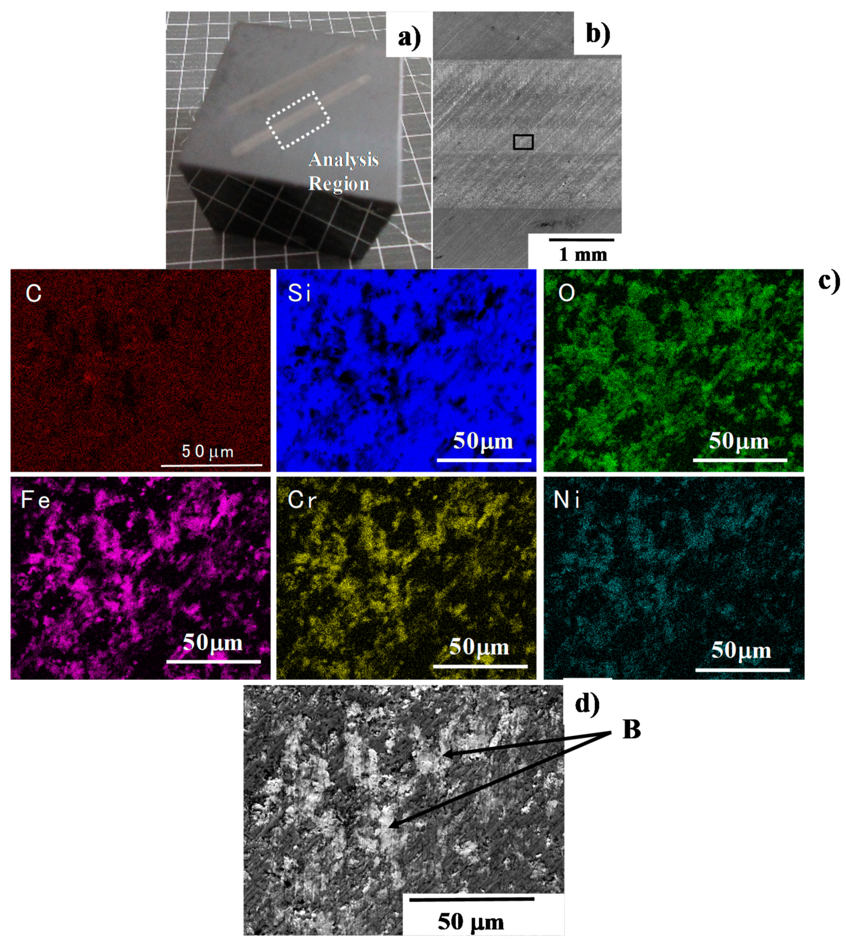
Figure 10.
SEM and electron-dispersive X-ray (EDX) analyses at the vicinity of the center of the contact interface between the SiC-coated punch and the AISI316 wire after forging by 10 shots up to the reduction of diameter by 40%. (a) Optical microscopic image on the SiC coating punch surface; (b) SEM image in low magnification on the contact interface of the SiC coating; (c) element mapping by C, Si, O, Fe, Ni and Cr and (d) SEM image on the oxide fragment deposits at the center of the contact interface (pointed by “B”).
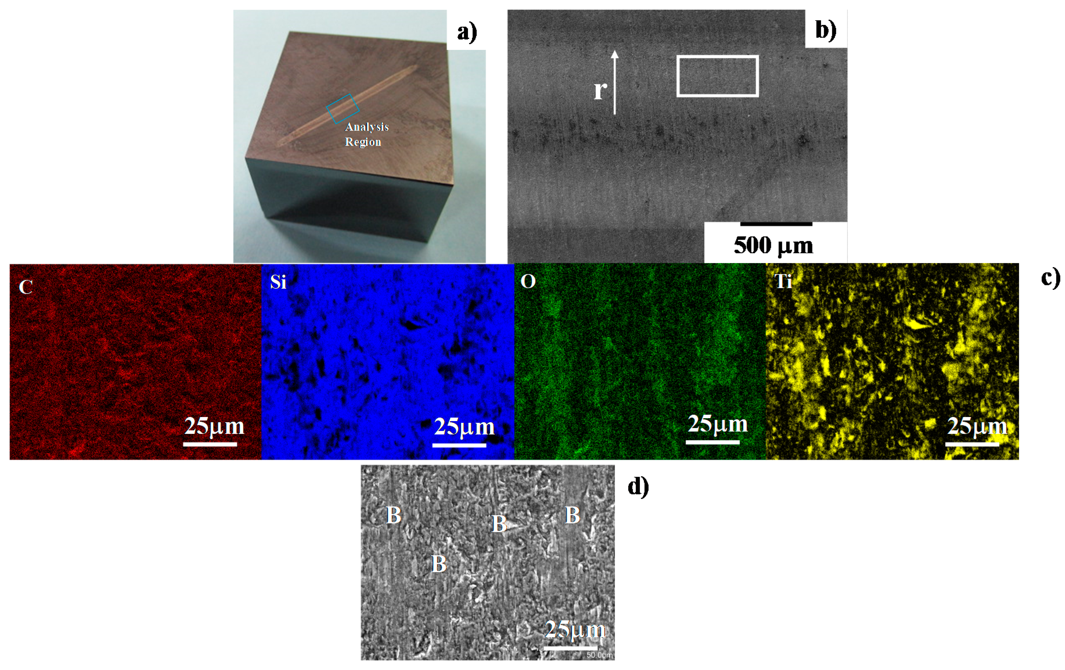
Figure 11.
SEM and EDX analyses away from the center of the contact interface between the SiC-coated punch and the titanium wire after forging by 10 shots up to the reduction of the diameter by 35%. (a) Optical microscopic image on the SiC coating punch surface; (b) SEM image in low magnification on the contact interface of the SiC coating; (c) element mapping by C, Si, O and Ti and (d) SEM image in high magnification away from the center, where “B” represents the titanium oxide deposits.
Figure 12.
SEM and EDX analyses at the vicinity of the center of the contact interface between the SiC-coated punch and the titanium wire after forging by 10 shots up to the reduction of the diameter by 35%. (a) Optical microscopic image on the SiC coating punch surface; (b) SEM image in low magnification on the contact interface of the SiC coating; (c) element mapping by C, Si, O and Ti and (d) SEM image in high magnification at the center of the contact interface, where “A” indicates the high carbon concentration and “B” represents the titanium oxide deposits.
© 2020 by the authors. Licensee MDPI, Basel, Switzerland. This article is an open access article distributed under the terms and conditions of the Creative Commons Attribution (CC BY) license (http://creativecommons.org/licenses/by/4.0/).


