Article

AlGaN/GaN Metal Oxide Semiconductor High-Electron Mobility Transistors with Annealed TiO2 as Passivation and Dielectric Layers

1
Department of Materials Science and Engineering, National Dong Hwa University, Hualien 974301, Taiwan
2
Department of Opto-Electronic Engineering, National Dong Hwa University, Hualien 974301, Taiwan
*
Author to whom correspondence should be addressed.
Micromachines 2023, 14(6), 1183; https://doi.org/10.3390/mi14061183
Submission received: 14 May 2023 / Revised: 28 May 2023 / Accepted: 30 May 2023 / Published: 31 May 2023
(This article belongs to the Special Issue III-V/III-N Materials and Devices)

Abstract

:
This paper reports on improved AlGaN/GaN metal oxide semiconductor high-electron mobility transistors (MOS-HEMTs). TiO2 is used to form the dielectric and passivation layers. The TiO2 film is characterized using X-ray photoemission spectroscopy (XPS), Raman spectroscopy, and transmission electron microscopy (TEM). The quality of the gate oxide is improved by annealing at 300 °C in N2. Experimental results indicate that the annealed MOS structure effectively reduces the gate leakage current. The high performance of the annealed MOS-HEMTs and their stable operation at elevated temperatures up to 450 K is demonstrated. Furthermore, annealing improves their output power characteristics.

1. Introduction

High-electron mobility transistors (HEMTs) have been intensively investigated over a long period. GaN has the favorable properties of a big bandgap, an enhanced breakdown electric field, and high thermal conductivity. AlGaN/GaN is a key material system in fifth generation (5G) applications in the field of microwave communication [1,2,3,4]. An AlGaN/GaN heterostructure generates a high two-dimensional electron gas (2-DEG) by spontaneous and piezoelectric polarization effects [5,6].
Ibbetson et al. presented a surface donor model to explain the origin of 2-DEG in an AlGaN/GaN heterojunction [7]. Generally, 2-DEG electrons are formed when the thickness of the AlGaN layer is larger than the critical value. Polarization phenomena in the AlGaN/GaN structures generate surface states. The donor-like states (positively charged surfaces) can trap the negative charges and thereby generate a virtual gate, which reduces the 2-DEG concentration [5,6]. Moderate surface passivation can prevent the appearance of the virtual gate. Another issue associated with the AlGaN/GaN HEMT is the high leakage currents through the Schottky gate. Inserting a gate dielectric can significantly reduce the gate’s leakage. The use of many insulators with a high dielectric constant to reduce the leakage current and prevent the significantly negative shift of the threshold voltage has been investigated. Particular insulators have been intensively examined. They include the insulating dielectric materials AlOX [8], Al2O3 [9,10,11,12,13,14,15], TiO2 [15,16,17,18], ZrO2 [19,20], SiNX [21], and SiO2 [22,23,24]. TiO2 has high dielectric constants, making TiO2 an excellent insulating material for use in MOS devices. Little has been published on GaN-based MOS-HEMTs with a TiO2 insulating layer, about which much remains unknown.
The effects of high temperature and surface passivation on GaAs-based HEMTs have been extensively examined [25]. However, few studies of the potential of AlGaN/GaN metal oxide semiconductor high-electron mobility transistors (MOS-HEMTs) for high-temperature operation have been undertaken. In our previous report, the threshold voltage (Vth), interface traps (Dit), unity current gain cutoff frequency (fT), maximum frequency of oscillation (fmax), and minimum noise figure (NFmin) of the TiO2 AlGaN/GaN MOS-HEMTs were examined [17]. However, analyses of their constituent materials, their high-temperature output characteristics, and their power characteristics have not been discussed. Furthermore, to the best of our knowledge, no research has been performed on the power characteristics of TiO2 AlGaN/GaN MOS-HEMTs and their performance at high temperatures, which are worthy of investigation.
In this study, a material analysis of TiO2 is first conducted. X-ray photoemission spectroscopy (XPS) and Raman spectroscopy are used to characterize TiO2 films. Experimental results demonstrate that annealing improves the performance of MOS-HEMTs. The current–voltage characteristics of the MOS-HEMTs that are operated up to 450 K are measured.

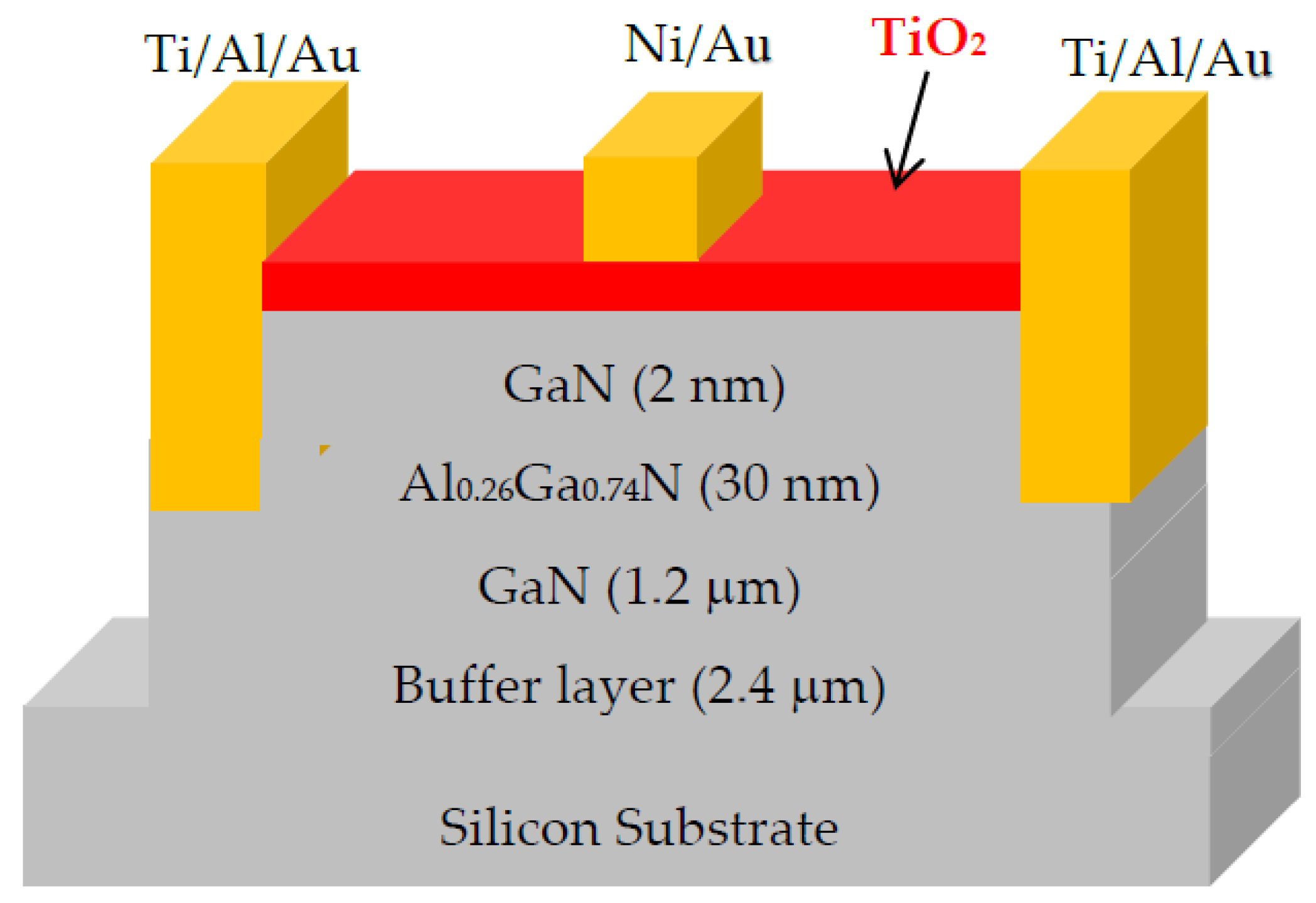
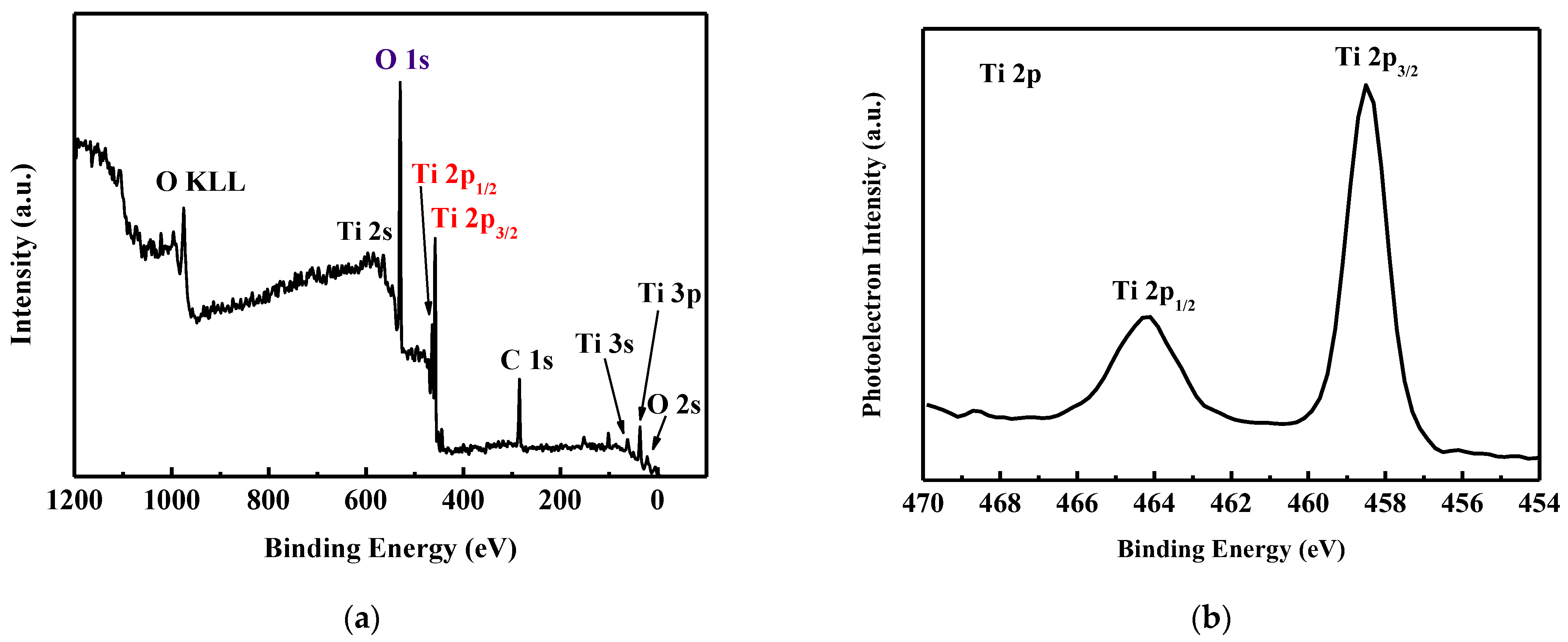
2. Fabrication and Structure of Device
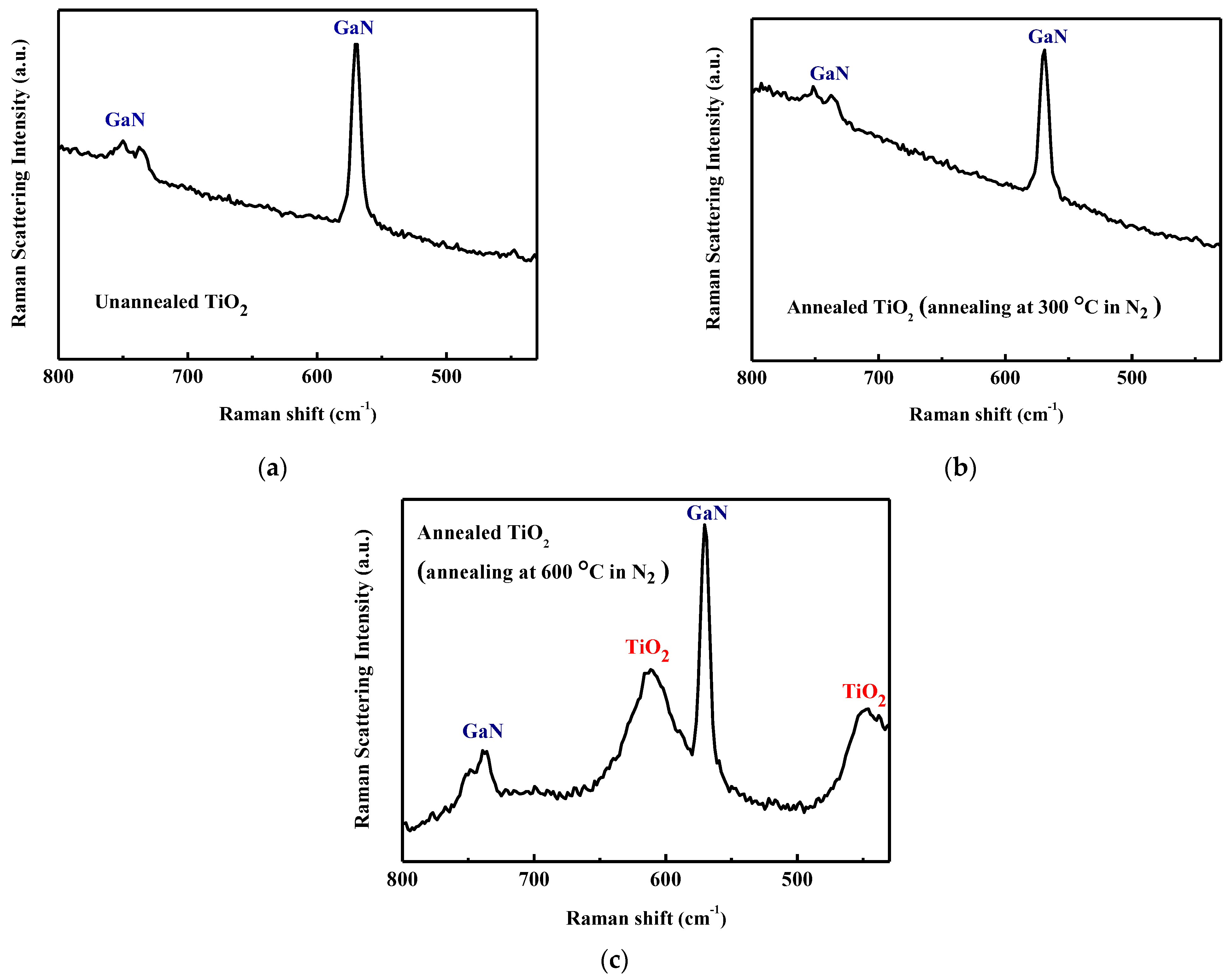
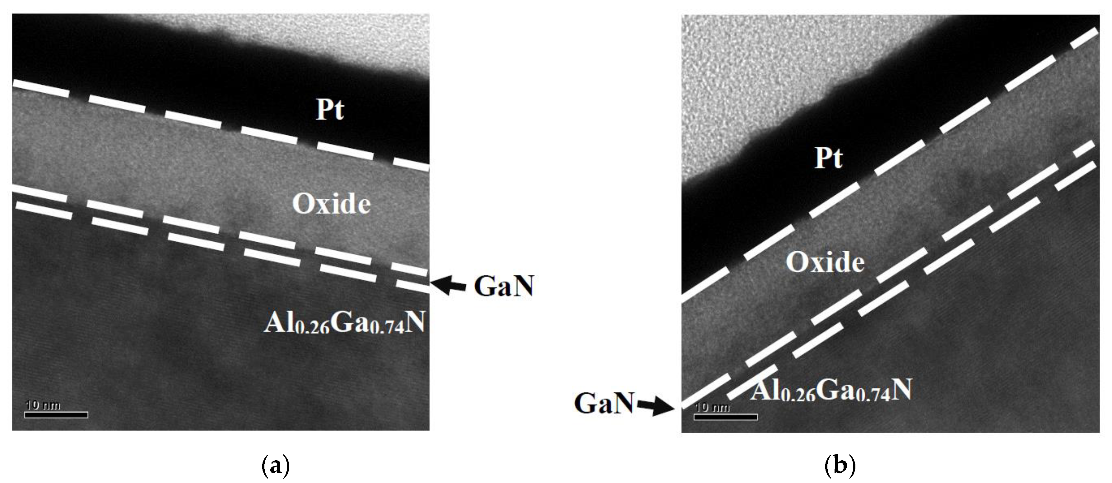
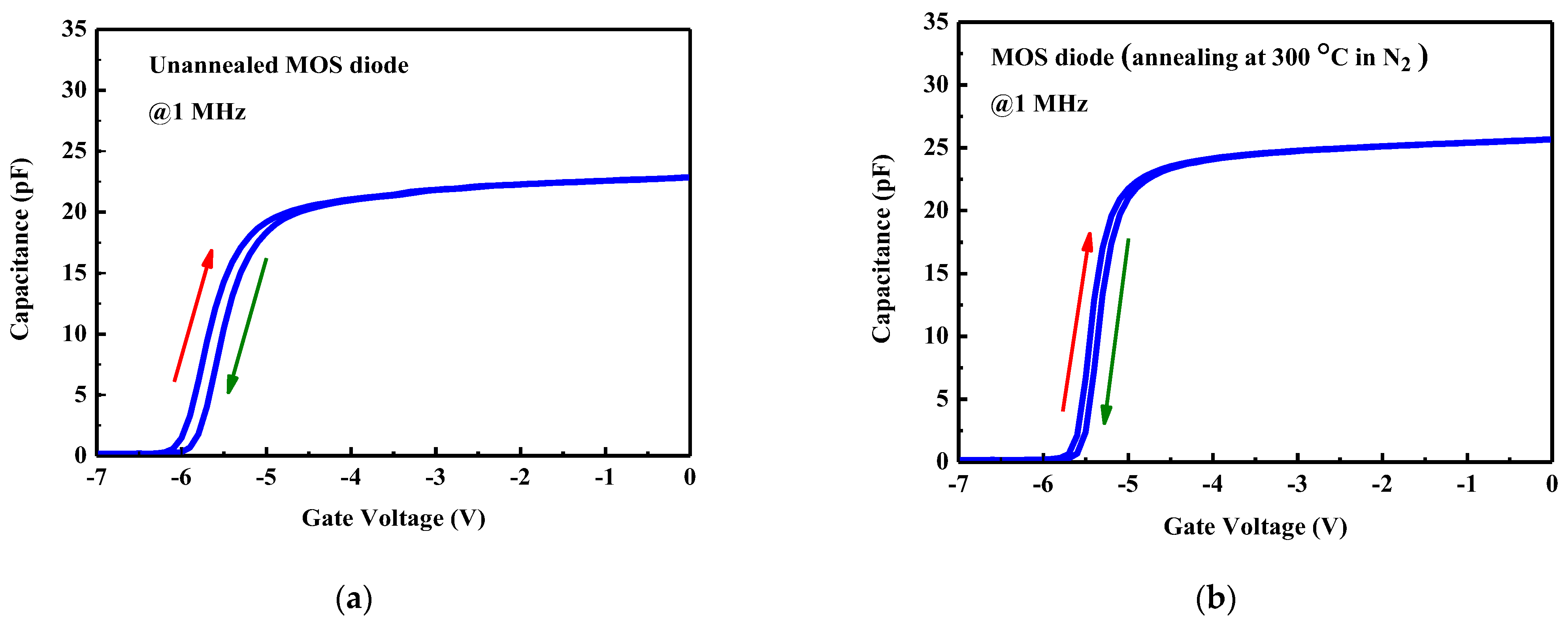
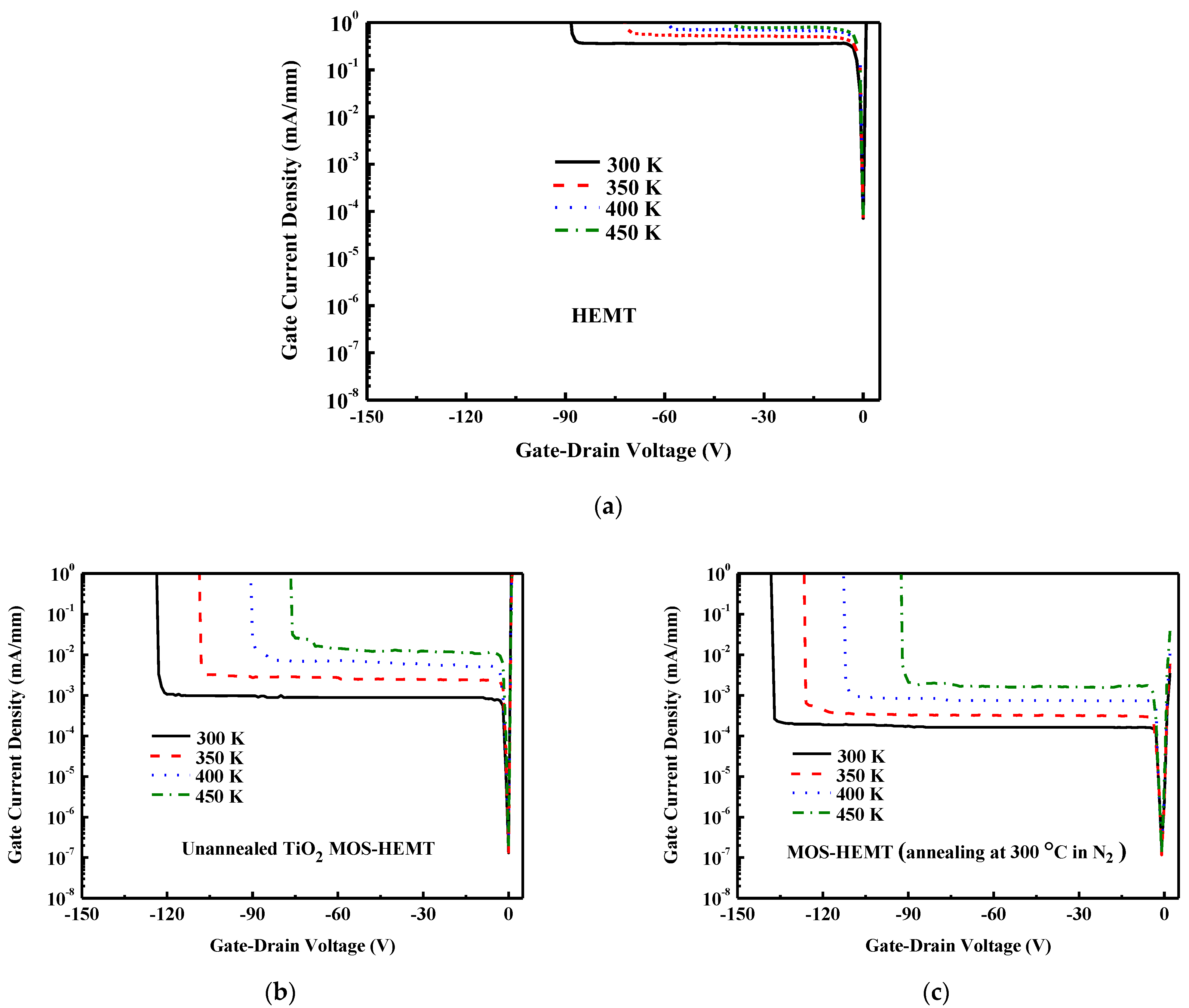
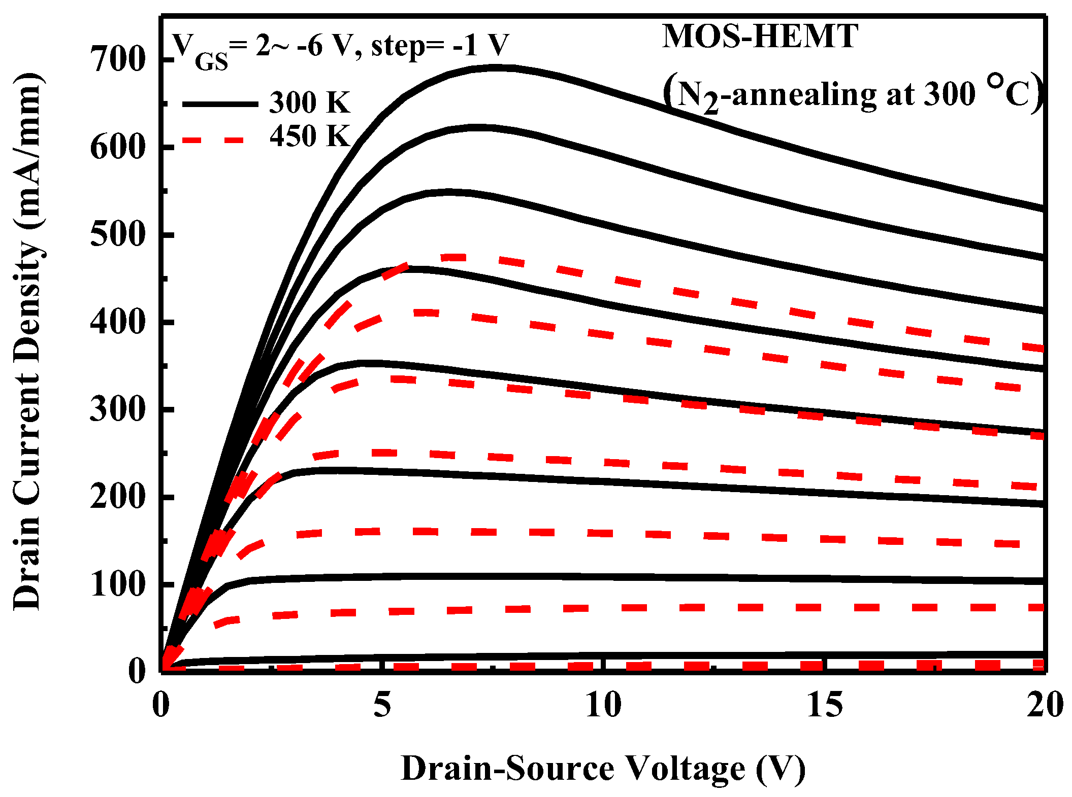
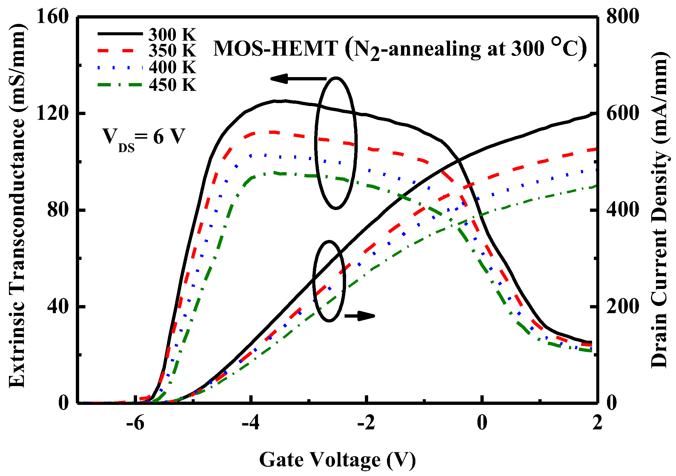
The epilayers of transistors were grown via low-pressure metal organic chemical vapor deposition (LP-MOCVD) on a silicon substrate. A typical AlGaN/GaN HEMT epitaxial structure that comprised of an undoped buffer layer, an undoped GaN layer (1.2 mm), an undoped Al0.26Ga0.74N top barrier layer (30 nm), and an undoped GaN cap layer (2 nm), was grown.
In order to generate the designed patterns, standard photolithography and lift-off techniques were used. First, the areas of mesa isolation were defined by inductively coupled plasma reactive ion etching (ICP-RIE), which is a means of dry etching. The purpose of mesa isolation is to reduce the leakage currents. Thermally evaporated Ni was used as the mesa etching mask. After the etching step, the Ni hard mask was removed completely using HNO3. Then, the source and drain contacts were formed by a Ti (10 nm)/Al (100 nm)/Au (50 nm) ohmic metal alloy. Finally, a Ni/Au (100/50 nm) gate metal stack was deposited without a recess or any extra dielectrics for the HEMT device. In this experiment, the device was spin-coated with positive photoresist (FH6400L) using a spinner. Ni has a high work function and so heightened the Schottky barrier. Au was used to prevent the oxidation of Ni.
A TiO2 layer was deposited in the access region of the MOS-HEMT after the source and drain ohmic contacts had completely formed. TiO2 was deposited using an RF sputtering system. The TiO2 target was prepared from 99.99% TiO2 powder. The substrate temperature was 25 °C. The reactive gas was a mixture of Ar and O2 with fixed flow rates of 20 sccm and 5 sccm, respectively. Etchant (NH4OH/H2O2/H2O = 1:2:1) was used to remove TiO2 from the source and drain region. In order to improve the quality of the TiO2 layer and reduce the oxide trap, the as-deposited TiO2 was put into a rapid thermal annealing (RTA) system. The gate length and width were 1 μm and 100 μm, respectively. Figure 1 schematically depicts the TiO2 AlGaN/GaN MOS-HEMT.

3. Results

Hall data were measured for the studied HEMT without passivation [17]. Experimental results demonstrate that unannealed TiO2 passivation increases the 2-DEG concentration and reduces electron mobility. The increase in the 2-DEG concentration is caused by the trapping of positive charges at the surface, neutralizing the polarization charge [5,6]. The electron mobility of the device with the annealed TiO2 passivation is higher than that achieved using unannealed TiO2 passivation. Annealing increases electron mobility by reducing the traps.
Figure 2a,b present typical XPS survey and high-resolution spectra of the as-deposited TiO2 films, respectively. Special attention should be paid to photoelectrons with binding energies between 454 eV and 470 eV. Figure 2b shows Ti 2p XPS data. The Ti 2p2/3 and Ti 2p1/2 spin-orbital splitting photoelectrons are located at around 458.5 eV and 464.2 eV, respectively, consistent with the values that are reported for TiO2 films [26,27,28].
Raman spectroscopy is a powerful diagnostic tool in the study of TiO2. Raman spectroscopy measurements are made. A TiO2 film is grown on GaN. The laser output power is set to 7.23 mW with an excitation wavelength of 532 nm. Figure 3a presents the Raman spectra of the as-deposited TiO2 taken at room temperature. Peaks that are associated with the GaN film are observed [29,30]. Figure 3b,c show the TiO2 films that are annealed at 300 °C and 600 °C, respectively. In general, crystalline TiO2 can exist in three phases, which are anatase, rutile, and brookite. Visible peaks due to the crystalline TiO2 phase are not obtained experimentally from the as-deposited TiO2 [Figure 3a] or 300 °C-annealed TiO2 [Figure 3b]. The 600 °C-annealed TiO2 yields two additional peaks [Figure 3c]. The emission bands at 447 and 610 cm−1 are identified as Eg and A1g of the rutile structure, respectively [31,32,33]. Raman analysis shows that TiO2 remains amorphous when it is annealed at 300 °C but it adopts the rutile crystal structure when it is annealed at 600 °C. These Raman spectroscopic results are consistent with our previously reported X-ray diffraction (XRD) analysis [17].
Transmission electron microscopy (TEM) samples are prepared using the focused ion beam (FIB) lift-out technique. Figure 4a,b display cross-sectional transmission electron micrographs of the TiO2/GaN/AlGaN heterostructure without and following annealing at 300 °C in an N2 ambient, respectively. The thickness of the 300 °C N2-annealed TiO2 film is about 14.7 nm. The thickness of the as-deposited TiO2 film is about 16.0 nm.
Gate oxide quality is evaluated using capacitance–voltage (C–V) measurements. The radius of the Schottky or MOS contact is 50.5 μm. Figure 5a,b are hysteresis plots of C–V data for the MOS capacitors without and following 300 °C annealing at 1 MHz, respectively. The C–V data are obtained by sweeping the gate voltage from zero to a negative value and back to zero. The 300 °C N2-annealed TiO2 MOS diode exhibits less hysteresis and a sharper transition from accumulation to depletion (or depletion to accumulation) than the unannealed MOS diode. Therefore, 300 °C N2 annealing improves the quality of the MOS diode [8,14,19,22,23]. From the zero-bias capacitance, the dielectric constant of the annealed TiO2 is calculated to be around 28.
Figure 6 plots the two-terminal gate-to-drain characteristics of the studied devices with a floating source that is operated at various temperatures. Figure 6b,c plot the results for the MOS-HEMT (without annealing) and MOS-HEMT (following N2 annealing at 300 °C), respectively. The breakdown voltage decreases as the temperature increases. Furthermore, the leakage current increases with temperatures. The 300 °C N2-annealed MOS-HEMT has a smaller leakage current than the unannealed MOS-HEMT under the same ambient condition because annealing reduces trap-assisted tunneling and Frenkel–Poole emission [34]. Experimental results clearly demonstrate the potential of our 300 °C N2-annealed MOS-HEMTs for high-temperature use.
Figure 7 plots the IDS–VDS characteristics of the 300 °C N2-annealed MOS-HEMT. The data are measured at 300 K and 450 K. The gate voltage is swept from VGS = +2 V to −6 V in −1 V steps. The drain current decreases as the temperature increases. Figure 8 plots the transfer characteristics and extrinsic transconductance of the 300 °C N2-annealed MOS-HEMT over a wide range of temperatures. The maximum extrinsic transconductane declines as the temperature increases. MOS-HEMTs operate stably at elevated temperatures up to 450 K with excellent pinch-off characteristics.
Figure 9 plots the measured CW power performance of the devices herein. Due to its lower gate leakage current, the maximum drain voltage of the MOS-HEMT could be higher than that of the HEMT, further favoring a high maximum rf power. The maximum output power (Pout) and power-added efficiency (PAE) in Class A operation are given by [35].
P o u t = 1 8 I D S , max ( V B V D s a t )
PAE   ( in   percentage ) = P o u t ( r f ) P i n ( r f ) P i n ( d c ) × 100 %
where IDS,max is the maximum drain current, VB is the breakdown voltage, Pin (dc) is the dc power dissipation, Pin (rf) is the input power, and Pout (rf) is the output power. Table 1 compares the large-signal performances of the studied devices. The 300 °C N2-annealed MOS-HEMT exhibits the best power characteristics owing to the improved IDS,max, reduced leakage current, and improved breakdown voltage.

4. Conclusions

AlGaN/GaN MOS-HEMTs with TiO2 as the insulating layer are investigated. The effects of annealing treatment on the crystal structure of TiO2 are examined. The annealed TiO2/AlGaN/GaN MOS-HEMT exhibits the smallest leakage current and largest output power characteristics of the studied devices, and has great promise for 5G applications.

Author Contributions

Investigation, Y.-S.L.; data curation, C.-C.L.; writing—original draft preparation, Y.-S.L.; writing—review and editing, Y.-S.L. All authors have read and agreed to the published version of the manuscript.

Funding

This research was funded by the National Science and Technology Council, Taiwan, grant number MOST 111-2221-E-259-013.

Conflicts of Interest

The authors declare no conflict of interest.

References

  1. Tsai, J.H.; Chiang, C.C.; Wang, F.M. High-Performance AlGaN/AlN/GaN High Electron Mobility Transistor with Broad Gate-to-Source Operation Voltages. Phys. Status Solidi C 2015, 12, 596–599. [Google Scholar] [CrossRef]
  2. Wang, T.B.; Hsu, W.C.; Su, J.L.; Hsu, R.T.; Wu, Y.H.; Lin, Y.S.; Su, K.H. Comparison of Al0.32Ga0.68N/GaN Heterostructure Field-Effect Transistors with Different Channel Thicknesses. J. Electrochem. Soc. 2007, 154, H131–H133. [Google Scholar] [CrossRef]
  3. Lin, Y.S.; Goa, W.H. High-Temperature Stability of Improved AlGaN/AlN/GaN HEMT with Pre-Gate Metal Treatment. IEICE Electron. Express 2019, 16, 20181046. [Google Scholar] [CrossRef]
  4. Lin, Y.S.; Lin, S.F. Large-signal Linearity and High-Frequency Noise of Passivated AlGaN/GaN High-Electron Mobility Transistors. Micromachines 2021, 12, 7. [Google Scholar] [CrossRef]
  5. Long, R.D.; McIntyre, P.C. Surface Preparation and Deposited Gate Oxides for Gallium Nitride Based Metal Oxide Semiconductor Devices. Materials 2012, 5, 1297–1335. [Google Scholar] [CrossRef]
  6. Vetury, R.; Zhang, N.Q.; Keller, S.; Mishra, U.K. The Impact of Surface States on the DC and RF Characteristics of AlGaN/GaN HFETs. IEEE Trans. Electron Devices 2001, 48, 560–566. [Google Scholar] [CrossRef]
  7. Ibbetson, J.P.; Fini, P.T.; Ness, K.D.; DenBaars, S.P.; Speck, J.S.; Mishra, U.K. Polarization Effects, Surface States, and the Source of Electrons in AlGaNÕGaN Heterostructure Field Effect Transistors. Appl. Phys. Lett. 2000, 77, 250–252. [Google Scholar] [CrossRef]
  8. Hahn, H.; Alam, A.; Heuken, M.; Kalisch, H.; Vescan, A. Investigation of Plasma-Oxidized Aluminium as a Gate Dielectric for AlGaN/GaN MISHFETs. Semicond. Sci. Technol. 2012, 27, 062001. [Google Scholar] [CrossRef]
  9. Taking, S.; MacFarlane, D.; Wasige, E. AlN/GaN MOSHEMTs with Thermally Grown Al2O3 Passivation. IEEE Trans. Electron Devices 2011, 58, 1418–1424. [Google Scholar] [CrossRef]
  10. Zhou, Q.; Chen, B.; Jin, Y.; Huang, S.; Wei, K.; Liu, X.; Bao, X.; Mou, J.; Zhang, B. High-Performance Enhancement-Mode Al2O3/AlGaN/GaN-on-Si MISFETs with 626 MW/cm2 Figure of Merit. IEEE Trans. Electron Devices 2015, 62, 776–781. [Google Scholar] [CrossRef]
  11. Gao, S.; Zhou, Q.; Liu, X.; Wang, H. Breakdown Enhancement and Current Collapse Suppression in AlGaN/GaN HEMT by NiOX/SiNX and Al2O3/SiNX as Gate Dielectric Layer and Passivation Layer. IEEE Electron Device Lett. 2019, 40, 1921–1924. [Google Scholar] [CrossRef]
  12. Kanaga, S.; Dutta, G.; Kushwah, B.; DasGupta, N.; DasGupta, A. Low Temperature and High Pressure Oxidized Al2O3 as Gate Dielectric for AlInN/GaN MIS-HEMTs. IEEE Trans. Device Mater. Reliab. 2020, 60, 613–621. [Google Scholar] [CrossRef]
  13. Lin, Y.S.; Wang, H.W. AlGaN/GaN Metal-Oxide-Semiconductor High-Electron Mobility Transistor with Annealed Al2O3 Gate Dielectric. Sci. Adv. Mater. 2022, 14, 1419–1422. [Google Scholar] [CrossRef]
  14. Blaho, M.; Gregušová, D.; Jurkovič, M.; Haščík, Š.; Fedor, J.; Kordoš, P.; Fröhlich, K.; Brunner, F.; Cho, M.; Hilt, O.; et al. Ni/Au-Al2O3 gate stack prepared by low-temperature ALD and lift-off for MOS HEMTs. Microelectron. Eng. 2013, 112, 204–207. [Google Scholar] [CrossRef]
  15. Rawat, A.; Meer, M.; Surana, V.K.; Bhardwaj, N.; Pendem, V.; Garigapati, N.S.; Yadav, Y.; Ganguly, S.; Saha, D. Thermally Grown TiO2 and Al2O3 for GaN-Based MOS-HEMTs. IEEE Trans. Electron Devices 2018, 65, 3725–3731. [Google Scholar] [CrossRef]
  16. Campbell, S.A.; Gilmer, D.C.; Wang, X.C.; Hsieh, M.T.; Kim, H.S.; Gladfelter, W.L.; Yan, J. MOSFET Transistors Fabricated with High Permitivity TiO2 Dielectrics. IEEE Trans. Electron. Devices 1997, 44, 104–109. [Google Scholar] [CrossRef]
  17. Lin, Y.S.; Lu, C.C. Improved AlGaN/GaN Metal-Oxide-Semiconductor High-Electron Mobility Transistors with TiO2 Gate Dielectric Annealed in Nitrogen. IEEE Trans. Electron Devices 2018, 65, 783–787. [Google Scholar] [CrossRef]
  18. Rawat, A.; Surana, V.K.; Meer, M.; Bhardwaj, N.; Ganguly, S.; Saha, D. Gate Current Reduction and Improved DC/RF Characteristics in GaN-Based MOS-HEMTs Using Thermally Grown TiO2 as a Dielectric. IEEE Trans. Electron Devices 2019, 66, 2557–2562. [Google Scholar] [CrossRef]
  19. Anderson, T.J.; Wheeler, V.D.; Shahin, D.I.; Tadjer, M.J.; Koehler, A.D.; Hobart, K.D.; Christou, A.; Kub, F.J.; Eddy, C.R., Jr. Enhancement Mode AlGaN/GaN MOS High-Electron-Mobility Transistors with ZrO2 Gate Dielectric Deposited by Atomic Layer Deposition. Appl. Phys. Express 2016, 9, 071003. [Google Scholar] [CrossRef]
  20. Jiang, H.; Tang, C.W.; Lau, K.M. Enhancement-Mode GaN MOS-HEMTs With Recess-Free Barrier Engineering and High-k ZrO2 Gate Dielectric. IEEE Electron Device Lett. 2018, 39, 405–408. [Google Scholar] [CrossRef]
  21. Meng, X.; Lee, J.; Ravichandran, A.; Byun, Y.C.; Lee, J.G.; Lucero, A.T.; Kim, S.J.; Ha, M.W.; Young, C.D.; Kim, J. Robust SiNx/GaN MISHEMTs with Crystalline Interfacial Layer Using Hollow Cathode PEALD. IEEE Electron Device Lett. 2018, 39, 1195–1198. [Google Scholar] [CrossRef]
  22. Lachab, M.; Sultana, M.; Fatima, H.; Adivarahan, V.; Fareed, Q.; Khan, M.A. Direct Current Performance and Current Collapse in AlGaN/GaN Insulated Gate High-Electron Mobility Transistors on Si (1 1 1) Substrate with Very thin SiO2 Gate Dielectric. Semicond. Sci. Technol. 2012, 27, 125001. [Google Scholar] [CrossRef]
  23. Husna, F.; Lachab, M.; Sultana, M.; Adivarahan, V.; Fareed, Q.; Khan, A. High-Temperature Performance of AlGaN/GaN MOSHEMT With SiO2 Gate Insulator Fabricated on Si (111) Substrate. IEEE Trans. Electron Devices. 2012, 59, 2424–2429. [Google Scholar] [CrossRef]
  24. Cho, G.; Cha, H.Y.; Kim, H. Influence of Oxygen–Plasma Treatment on In-Situ SiN/AlGaN/GaN MOSHEMT with PECVD SiO2 Gate Insulator. Materials 2019, 12, 3968. [Google Scholar] [CrossRef]
  25. Lin, Y.S.; Huang, J.J. Linearity Enhancement and Noise Reduction in a Passivated AlGaAs/InGaAs/GaAs High-Electron Mobility Transistor. J. Korean Phys. Soc. 2021, 79, 828–831. [Google Scholar] [CrossRef]
  26. McCa†erty, E.; Wightman, J.P. Determination of the Concentration of Surface Hydroxyl Groups on Metal Oxide Films by a Quantitative XPS Method. Surf. Interface Anal. 1998, 26, 549–564. [Google Scholar] [CrossRef]
  27. Alam, M.J.; Cameron, D.C. Preparation and Characterization of TiO2 Thin Films by Sol-Gel Method. J. Solgel Sci. Technol. 2002, 25, 137–145. [Google Scholar] [CrossRef]
  28. Wang, S.; Lian, J.S.; Zheng, W.T.; Jiang, Q. Photocatalytic Property of Fe Doped Anatase and Rutile TiO2 Nanocrystal Particles Prepared by Sol–Gel Technique. Appl. Surf. Sci. 2012, 263, 260–265. [Google Scholar] [CrossRef]
  29. Zhang, J.M.; Ruf, T.; Cardona, M.; Ambacher, O.; Stutzmann, M.; Wagner, J.-M.; Bechstedt, F. Raman Spectra of Isotopic GaN. Phys. Rev. B 1997, 56, 14399–14406. [Google Scholar] [CrossRef]
  30. Krishna, T.C.S.; Aggarwal, N.; Reddy, G.A.; Dugar, P.; Mishra, M.; Goswami, L.; Dilawar, N.; Kumar, M.; Mauryac, K.K.; Gupta, G. Probing the Correlation Between Structure, Carrier Dynamics and Defect States of Epitaxial GaN Film on (11 2 ¯ 0)Sapphire Grown by Rf-Molecular Beam Epitaxy. RSC Adv. 2015, 5, 73261–73267. [Google Scholar] [CrossRef]
  31. Balachandran, U.; Eror, N.G. Raman spectra of titanium dioxide. J. Solid State Chem. 1982, 42, 276–282. [Google Scholar] [CrossRef]
  32. Hsu, L.S.; Rujkorakarn, R.; Sites, J.R.; She, C.Y. Thermally Induced Crystallization of Amorphous-Titania Films. J. Appl. Phys. 1986, 59, 3475–3480. [Google Scholar] [CrossRef]
  33. Brange, K.; Ottermann, C.R.; Anderson, O.; Jeschkowski, U.; Laube, M.; Feile, R. Investigation of TiO2 Films Deposited by Different Techniques. Thin Solid Films 1991, 197, 279–285. [Google Scholar] [CrossRef]
  34. Turuvekere, S.; Karumuri, N.; Rahman, A.A.; Bhattacharya, A.; DasGupta, A.; DasGupta, N. Gate Leakage Mechanisms in AlGaN/GaN and AlInN/GaN HEMTs: Comparison and modeling. IEEE Trans. Electron Devices 2013, 60, 3157–3165. [Google Scholar] [CrossRef]
  35. Sze, S.M. High-Speed Semiconductor Devices; Wiley: New York, NY, USA, 1990; Chapter 4. [Google Scholar]
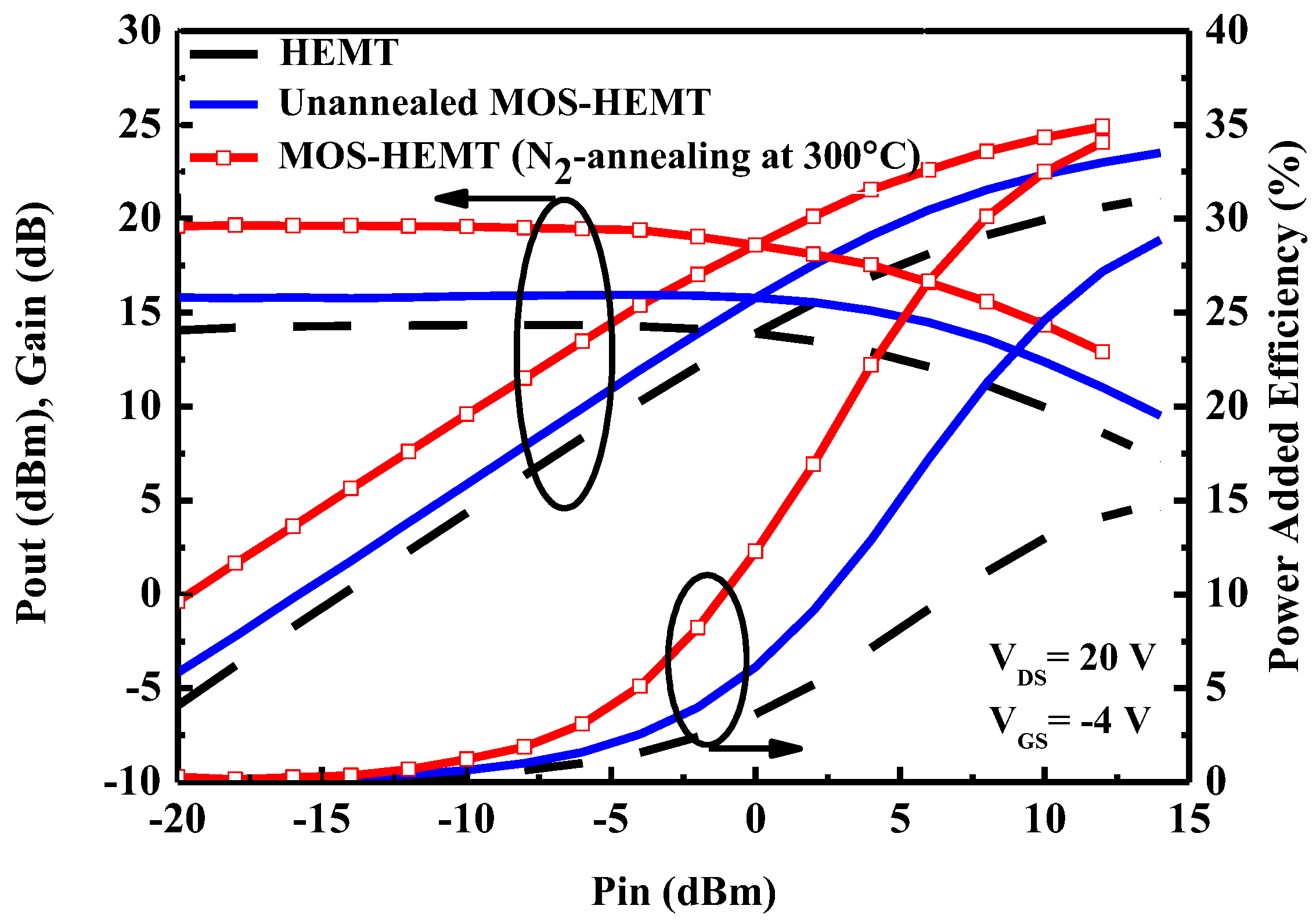
Figure 1. Schematic structure of TiO2 MOS-HEMT.
Micromachines 14 01183 g001
Figure 2. (a) XPS survey and (b) high-resolution XPS spectra of the as-deposited TiO2 films.
Micromachines 14 01183 g002
Figure 3. Raman spectra of (a) as-deposited, (b) 300 °C-annealed, and (c) 600 °C-annealed TiO2 on GaN.
Micromachines 14 01183 g003
Figure 4. Cross-sectional transmission electron micrographs of studied heterostructure (a) without annealing and (b) following annealing at 300 °C in N2 ambient.
Micromachines 14 01183 g004
Figure 5. Capacitance–voltage hysteresis plots of (a) as-deposited and (b) 300 °C N2-annealed TiO2 MOS capacitors.
Micromachines 14 01183 g005
Figure 6. Two-terminal gate–drain breakdown plots for (a) HEMT, (b) unannealed MOS-HEMT, and (c) annealed MOS-HEMT at various temperatures.
Micromachines 14 01183 g006
Figure 7. IDS–VDS characteristics of MOS-HEMT at various temperatures.
Micromachines 14 01183 g007
Figure 8. Drain current and extrinsic transconductance vs. gate-to-source voltage for studied devices at various temperatures.
Micromachines 14 01183 g008
Figure 9. Load-pull data of the studied devices at 300 K. Each device is biased to VDS = 20 V and VGS = −4 V, and measurements are made at 2.4 GHz.
Micromachines 14 01183 g009
Table 1. Comparison of 2.4 GHz large-signal performances of studied devices.
POUT (dBm)Gain (dB)PAE (%)
HEMT21.8914.3414.5
Unannealed MOS-HEMT23.5115.8228.88
MOS-HEMT (N2 annealing at 300 °C)24.9219.6534.08
Disclaimer/Publisher’s Note: The statements, opinions and data contained in all publications are solely those of the individual author(s) and contributor(s) and not of MDPI and/or the editor(s). MDPI and/or the editor(s) disclaim responsibility for any injury to people or property resulting from any ideas, methods, instructions or products referred to in the content.

