Abstract
This work outperforms the previous literatures by proposing a delay-cell-controlled voltage control oscillator (VCO) design for common unipolar, single-gate, and enhancement-mode thin-film transistor (TFT) technologies. A design example with InZnO TFTs is simulated to verify the proposed design. The design example has a 500 μW power consumption, 0.7 mm2 area, 3.8 kHz–8 kHz output frequency range, 600 Hz/V tuning sensitivity, and 4% maximum linear error. This design may have the potential to be used for flexible, low cost, and moderate speed sensor readout interfaces.
1. Introduction
Thin-film transistor (TFT) circuits have made great progress in recent years. Complicated circuits and systems including ARM processers [1], analog frontends and conversion circuits [2], and wireless communication systems [3] have been reported. Voltage control oscillators (VCOs) are an integral part of many electronic systems. Table 1 reviews the existing TFT-based VCO designs [4,5,6,7,8,9,10]. This work focuses on the digital ring oscillator (RO) architecture with delay-cell-control scheme since it has the advantages of the simple and compact structure, the high input impedance, the digital output that can be processed directly using digital circuitry without shaping, and it does not require analogue blocks such as high-performance operation amplifiers that are difficult to achieve with current TFT technologies. The delay-cell-control VCO design that was proposed for the first time in [6], however, was designed for the uncommon dual-gate and depletion-mode TFT device. This work solves this issue by presenting another design for the common TFT devices, i.e., unipolar (non-complementary), single-gate, and enhancement-mode TFTs.

Table 1.
Summary of the existing TFT VCO designs.
2. Device
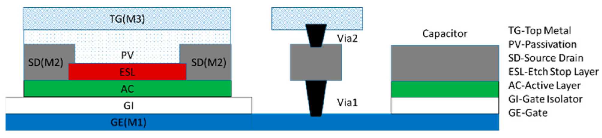
The design example was based on our 10 μm channel length, n-type, etch stop layer (ESL), and InZnO (IZO) TFTs. The device has a bottom gate and top contact structure on glass substrate as shown in Figure 1. Three metal layers are provided: the gate metal (M1), the source/drain metal (M2), and the top metal (M3) for further connection. The gate metal is a 200 nm thick molybdenum (Mo) layer (M1). The gate insulator (GI) is two stacked layers of SiNx/SiO2 with 200 nm/50 nm. The active layer is a 30 nm thick IZO. Source and drain electrodes are 200 nm thick Mo layers (M2). A 300 nm SiO2 is formed as a passivation layer (PV) for protecting the TFT devices. A layer of Ni serves as the contact electrode (M3). The typical threshold voltage (Vth), mobility, and subthreshold slope are 3 V, 10.5 cm2V−1s−1, and 110 mV/dec, respectively. Because of the bottom gate structure, overlapping capacitance per unit channel width is 1.41 nF/m. On-chip capacitors with 19 nF/cm2 are also available by using the M1 and M2 as two plates and the gate oxide as an insulating layer. More details about the TFT device technology can be found elsewhere [11].
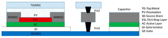
Figure 1.
The IZO TFT technology used.
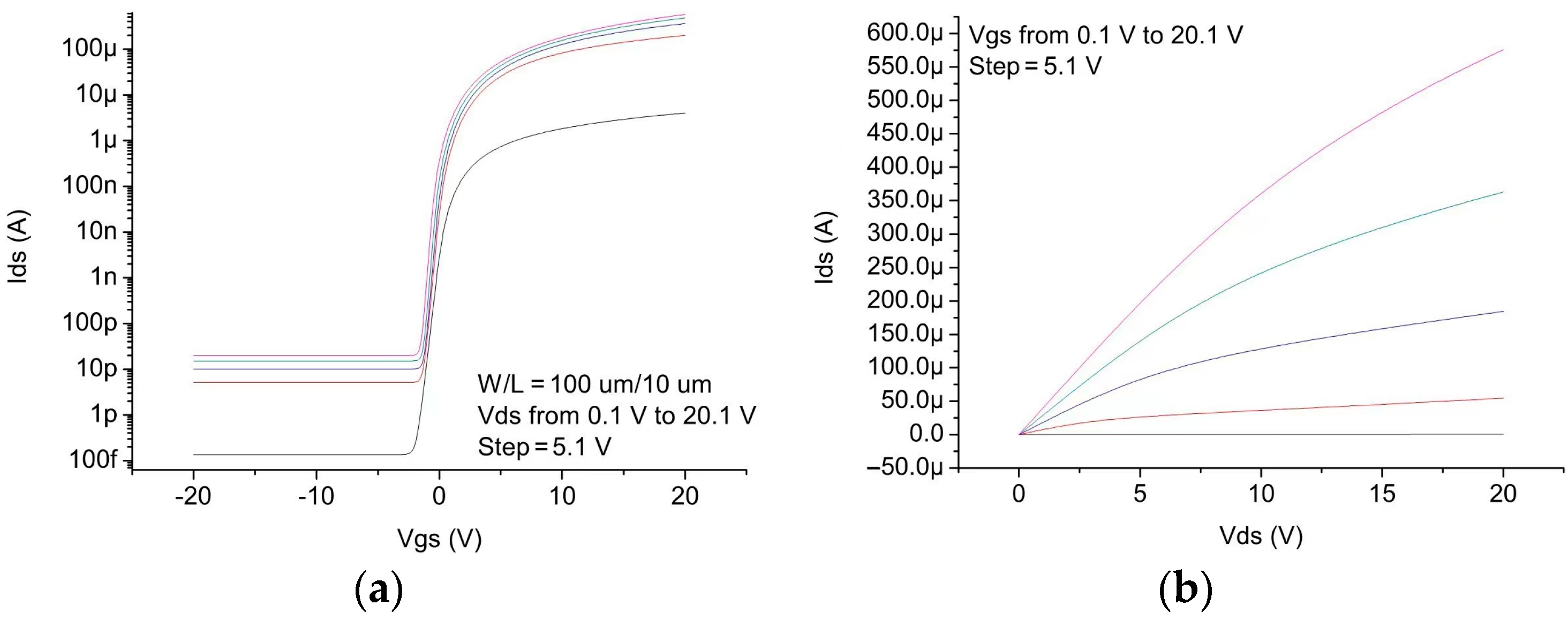
Characteristics of the TFT devices used are calibrated with experimental data [11]. An Hspice Level = 62 RPI Poly Si TFT Model is established using parameter extraction to fit the measured device characteristics. Figure 2 shows the simulated transfer and output curves of the device.
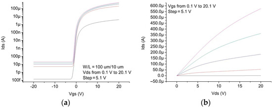
Figure 2.
Simulated (a) transfer and (b) output curves of the IZO TFT device.
3. Circuit Design
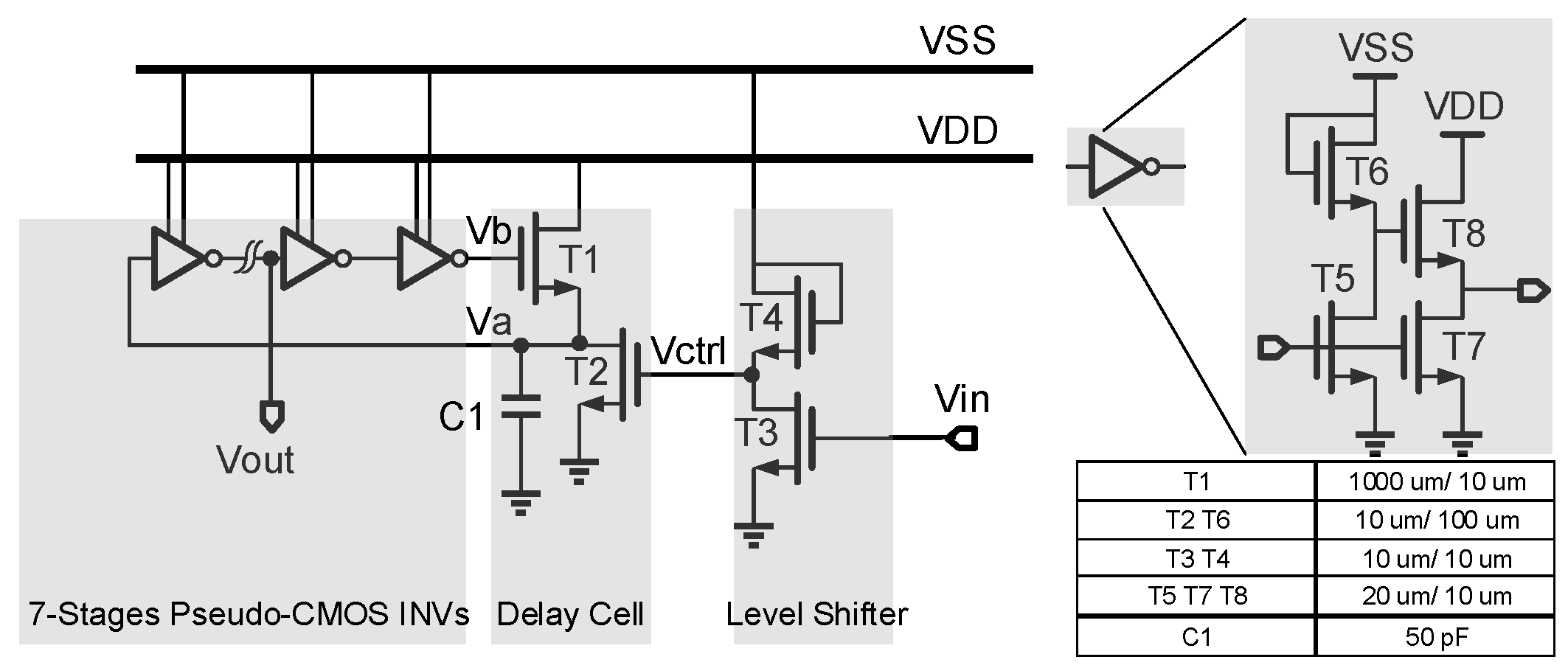
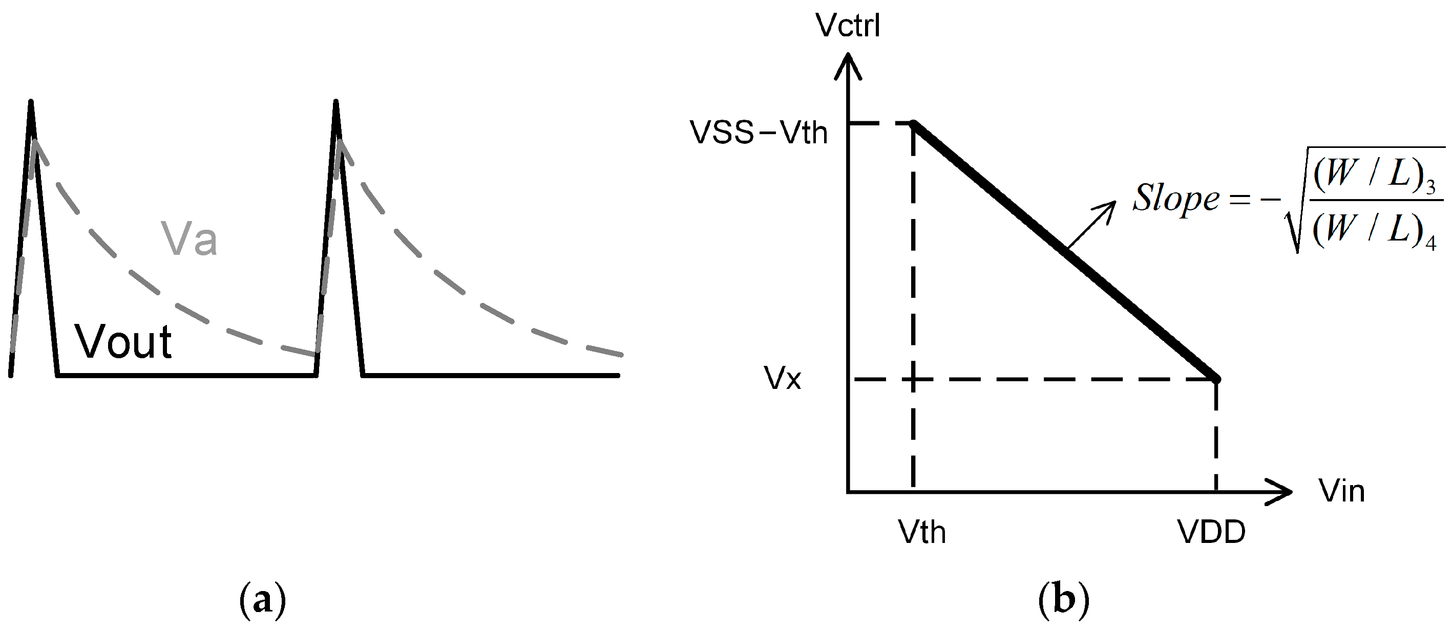
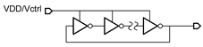
Figure 3 shows the schematic of the proposed VCO. It consists of a RO and a level shifter, while the RO consists of an odd number of inverters and a non-inverting delay cell. It generates self-oscillation with the frequency adjusted using a voltage control resistor realized through T2. The waveform of the delay cell output (node Va) is shaped using the inverter chains and becomes a series of pulses at the output node Vout. Typical waveforms of the circuit nodes are shown in Figure 4a.
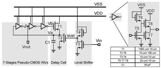
Figure 3.
Schematic of the proposed TFT VCO.
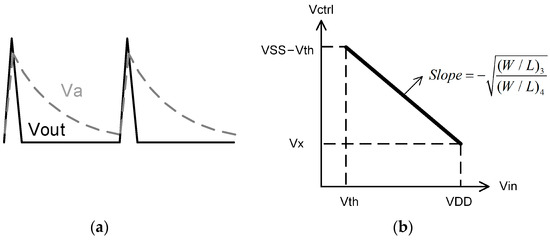
Figure 4.
(a) Qualitative sketch of the main waveforms of the proposed VCO, and (b) voltage transfer curve of the level shifter.
The delay cell consists of T1, T2, and C1. The rising time constant of the delay cell is proportional to R1C1 while C1 is charging through T1, and the falling time constant of the delay cell is proportional to R2C1 while C1 is discharging through T2, whereas R1 and R2 are equivalent resistances of T1 and T2, respectively. T1 and T2 are both biased in the deep linear region so that they can act as resistors. R2 is a voltage control resistor controlled using the gate voltage of T2, Vctrl, thus the oscillation period can be controlled using Vctrl. If the rising time and delay of the inverter chain are both much smaller than the falling time, the oscillation frequency can be proportional to Vcrtl, thus (W/L)1 is designed to be much greater than (W/L)2, to make R2 much greater than R1. Also, a relatively large capacitance is chosen. The oscillation period can be given using
where TINV is the inverter chain delay, TR is the rising time of the delay cell, TF is the falling time of the delay cell, and R2 is the equivalent resistance of T2.
The pull-down transistor T2 is designed to be biased in the deep linear region so that it can act as a voltage control resistor whose resistance is given by
Combining (1) and (2), the oscillation frequency is given using
To ensure T2 in the linear region, its gate voltage Vctrl should be higher than VDD-Vth. However, the input signal Vin ranges from GND to VDD, which cannot meet the requirement. Thus, a level shifter is designed to boost the Vin to above VDD-Vth.
The level shifter is actually a diode-load inverter or amplifier that is powered using VSS. Figure 4b gives the voltage transfer curve of the level shifter. When Vin increases from Vth to VDD, Vctrl linearly decreases from VSS−Vth to Vx. The slope of the transfer curve equals to . Thus, the transfer function of the level shifter is given using
To make sure that T3 is in the saturation region and T2 is in the linear region, Vx must be higher than VDD−Vth. Therefore, the sizes of T3 and T4 should satisfy
In this design, the VSS is set to be 2VDD [12], and T3 and T4 are designed to have the same size. Since its gain remains constant over the entire input range, the level shifter does not introduce linear errors into the VCO. Signals will be inverted after passing through the level shifter, so the input voltage and output frequency are ultimately inversely proportional.
Combining (3) and (4), we can give the final f-V characteristic using
The above formula can be further described as
where KVCO represents the tuning sensitivity and K is a scale constant.
In summary, the properties of the proposed VCO are described by (8) and (9), with the constraints described by (5) and (6).
One of the sources of the nonlinearity of the proposed VCO is the delay of the inverter chains and the rising time of the delay cell, as described in (1). Therefore, a large value of C1 and a small size of T2 are desired to achieve a high linearity. However, according to (8) and (9), this will reduce the output frequencies as well as the KVCO. A tradeoff between linearity, oscillation frequencies, and sensitivity is found in the proposed design. Another source of the nonlinearity derives from the deviation between the actual device characteristics and the square-law model that makes T2 not behave as an ideal voltage-controlled resistor.
4. Simulation Results and Discussion
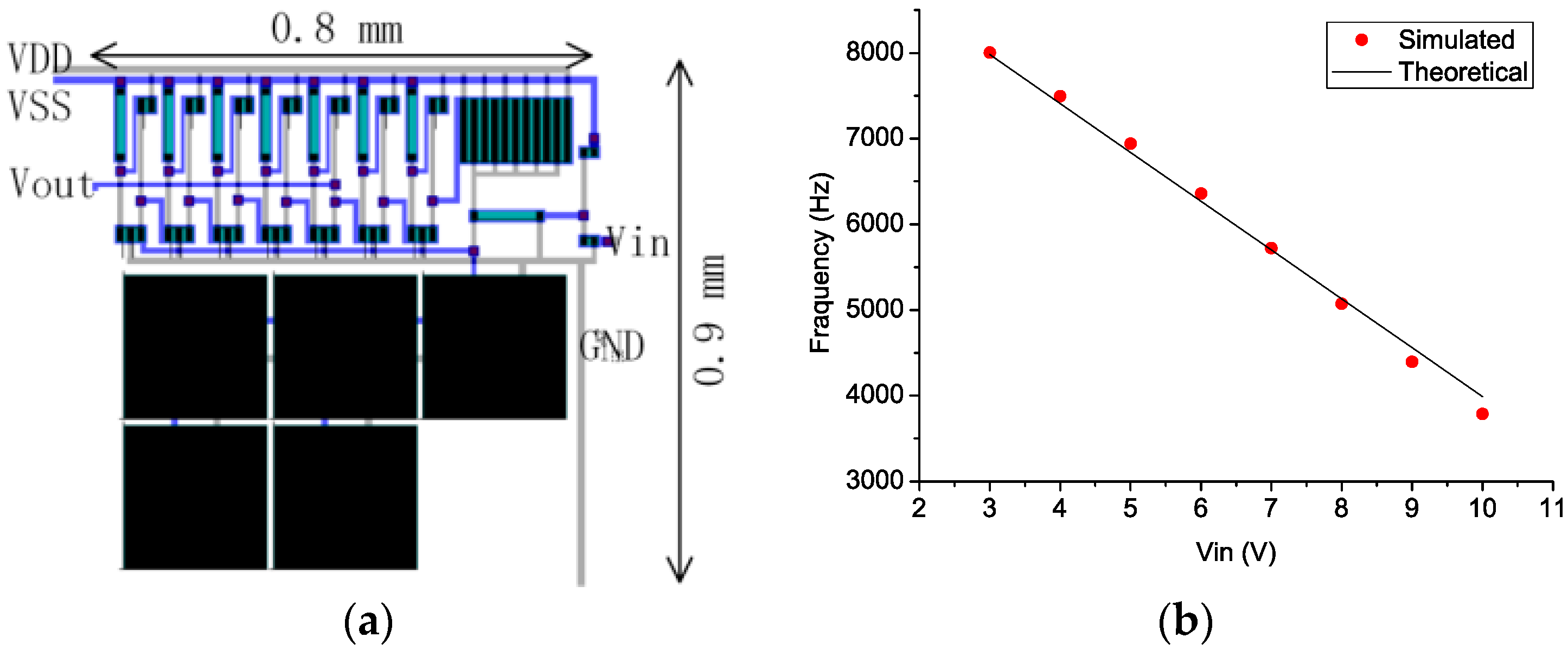
Figure 5a shows the layout of the proposed VCO. The VCO occupies 0.7 mm2 area fully on-chip and consumes 500 μW power.

Figure 5.
(a) Layout of the proposed VCO, and (b) simulated and theoretical V-f characteristics of the proposed VCO.
The simulations were performed under VDD = 10 V and VSS = 20 V. The reason for choosing these supply voltages is the relatively high Vth (~3 V) of our TFT devices. VCO outputs under different input voltages that range from Vth to VDD were captured.
Figure 5b shows the simulated voltage versus frequency curve of the VCO. The output frequency decreases from 8 kHz to 3.8 kHz as Vin increases from 3 V to 10 V.
Theoretical curves that are calculated (8) using KVCO of −570, VSS of 20 V, and Vth of 3V, are also shown in Figure 5b. It is found that the theoretical curve fits well with the simulated curve. This means that the theoretical analysis does provide an accurate prediction of circuit behavior. Differences between simulated and theoretical characteristics result from the deviation between the actual device characteristics and the square-law model.
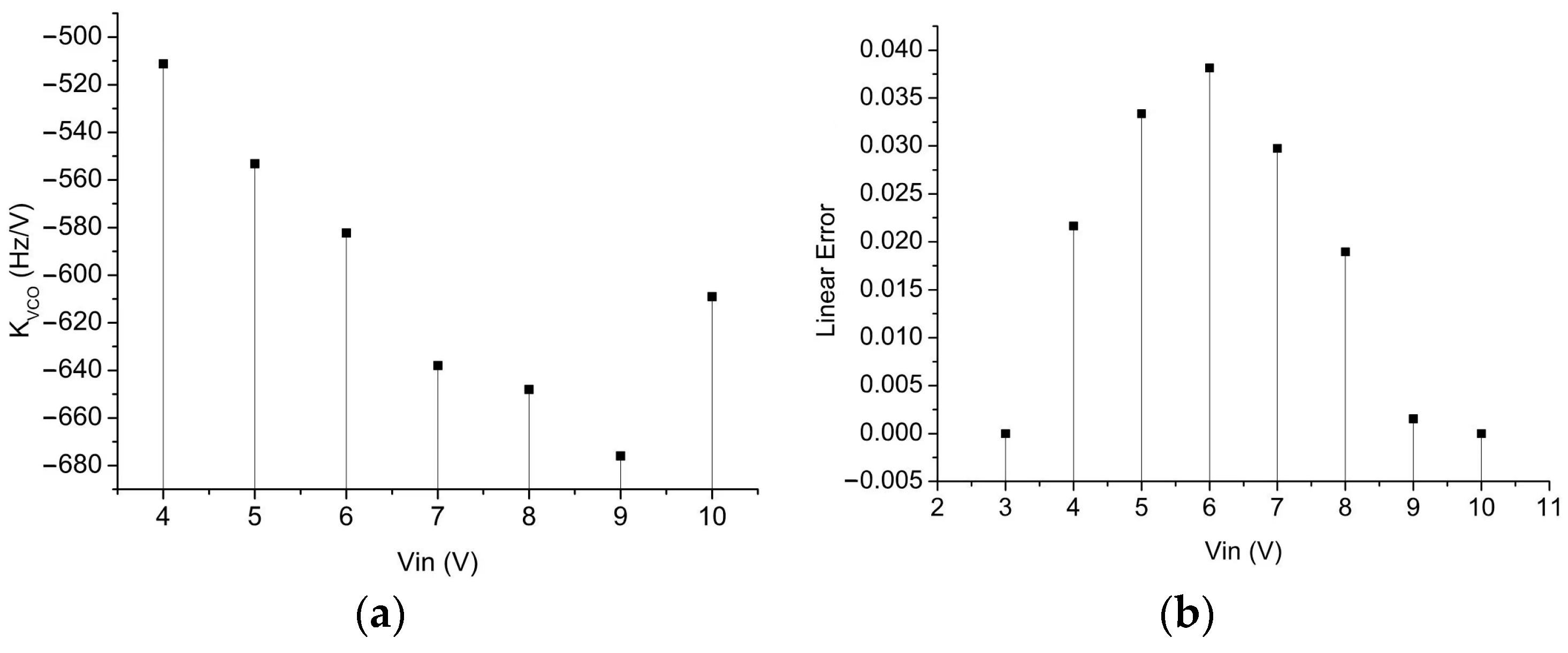
Figure 6a shows the voltage versus KVCO curve of the VCO. The value of KVCO ranges from 510 Hz/V to 680 Hz/V. The average value of KVCO is 600 Hz/V. Figure 6b shows the linear error of the VCO that was normalized using the output frequency range. The maximum linear error is 4% and appears at Vin = 6 V. The linear error is calculated as the difference between the measured f-V curve and the linear fit through its extremes.

Figure 6.
Simulated (a) KVCO and (b) linear error of the proposed VCO.
Table 2 summarizes the performance of the proposed VCO and compares it to the state-of-the-art counterparts. This work outperforms [6] by proposing a design suitable for the single-gate and enhancement TFT devices. Moderate output frequencies and tuning sensitivity are achieved, due to the inherent speed–linearity trade-off of the proposed design. In addition, excellent circuit integration and power consumption are performed, thanks to the compact and all-digital architecture. According to these results, it is suggested that the proposed design may have the potential to be used for low-cost, moderate speed applications such as voltage-to-frequency converters for flexible sensor interfaces.
Table 2.
Summary and comparison table.
5. Conclusions
A delay-controlled VCO design for unipolar, single-gate, and enhancement-mode TFT technologies has been proposed. Theoretical analysis and design guidelines have been given. A design example based on IZO TFTs has been proposed to verify the design. It is found that the simulation results of the design example fit well with the theoretical analysis, showing moderate speed and linearity, excellent integration, and power consumption compared to the literatures.
Author Contributions
Conceptualization, B.L. and M.Z.; Funding Acquisition, B.L.; Supervision, B.L. and Z.W.; Formal Analysis S.W. and Y.X.; Software, S.W.; Writing—original draft, S.W. and Y.X.; Methodology, Z.W. and M.Z.; Writing—review & editing, Z.W. and R.C.; Project administration, R.C. and M.Z.; Validation, R.C.; Data curation, Y.X. All authors have read and agreed to the published version of the manuscript.
Funding
This work was supported in part by National Natural Science Foundation of China under Grant 62174058, in part by the Guangdong Basic and Applied Basic Research Foundation under Grant 2020B1515120022 and Grant 2019A1515011820, in parted by the Key-Area Research and Development Program of Guangdong Province 2021B0101280001, in part by the Science and Technology Program of Guangdong Province under Grant 2021A0505110009, in part by the Program for Guangdong High-Level Talents, and in part by the Ji Hua Laboratory scientific research project under Grant X190221TF190.
Institutional Review Board Statement
Not applicable.
Informed Consent Statement
Not applicable.
Data Availability Statement
Not applicable.
Conflicts of Interest
The authors declare no conflict of interest.
References
- Biggs, J.; Myers, J.; Kufel, J.; Ozer, E.; Craske, S.; Sou, A.; Ramsdale, C.; Williamson, K.; Price, R.; White, S. A natively flexible 32-bit arm microprocessor. Nature 2021, 595, 532–536. [Google Scholar] [CrossRef] [PubMed]
- Zulqarnain, M.; Stanzione, S.; Rathinavel, G.; Smout, S.; Willegems, M.; Myny, K.; Cantatore, E. A flexible ECG patch compatible with NFC RF communication. NPJ Flex. Electron. 2020, 4, 1–8. [Google Scholar] [CrossRef]
- Meister, T.; Ishida, K.; Carta, C.; Munzenrieder, N.; Ellinger, F. Flexible Electronics for Wireless Communication: A Technology and Circuit Design Review with an Application Example. IEEE Microw. Mag. 2022, 23, 24–44. [Google Scholar] [CrossRef]
- Ramkumar, G.; Jürgen, K.; Klaus, L.; Glesner, M. Investigation of voltage-controlled oscillator circuits using organic thin-film transistors (OTFT) for use in VCO-based analog-to-digital converters. Solid-State Electron. 2014, 93, 8–14. [Google Scholar]
- Sun, W.Y.; Zhao, Q.H.; Qiao, F.; Liu, Y.; Yang, H.; Guo, X.; Zhou, L.; Wang, L. An 8b 0.8kS/s configurable VCO-based ADC using oxide TFTs with Inkjet printing interconnection. In Proceedings of the 2017 IEEE International Symposium on Circuits and Systems (ISCAS), Baltimore, MD, USA, 28–31 May 2017. [Google Scholar]
- Raiteri, D.; van Lieshout, P.; van Roermund, A.; Cantatore, E. An Organic VCO-Based ADC for Quasi-Static Signals Achieving 1LSB INL at 6b Resolution. In Proceedings of the IEEE International Solid-State Circuits Flagship Conference of the IEEE Solid-State-Circuits-Society (ISSCC), San Francisco, CA, USA, 17–21 February 2013. [Google Scholar]
- Li, H.; Deng, S.; Xu, Y.; Zhong, W.; Luo, D.; Li, G.; Kwok, H.S.; Chen, R. A Differential Ring Oscillator with Tail Current Source Control Scheme Using N-Type Oxide TFTs. IEEE Trans. Electron Devices 2022, 69, 1870–1875. [Google Scholar] [CrossRef]
- Xu, Y.; Zhong, W.; Li, B.; Deng, S.; Fan, H.; Wu, Z.; Lu, L.; Yeung, F.S.Y.; Kwok, H.S.; Chen, R. An Integrator and Schmitt Trigger Based Voltage-to-Frequency Converter Using Unipolar Metal-Oxide Thin Film Transistors. IEEE J. Electron Devices Soc. 2021, 9, 144–150. [Google Scholar] [CrossRef]
- Keragodu, T.; Tiwari, B.; Bahubalindruni, P.; Goes, J.; Barquinha, P. A Voltage Controlled Oscillator Using IGZO Thin-Film Transistors. In Proceedings of the 2018 IEEE International Symposium on Circuits and Systems (ISCAS), Florence, Italy, 27–30 May 2018. [Google Scholar]
- Meister, T.; Ishida, K.; Knobelspies, S.; Cantarella, G.; Münzenrieder, N.; Tröster, G.; Carta, C.; Ellinger, F. 5–31-Hz 188-μW Light-Sensing Oscillator with Two Active Inductors Fully Integrated on Plastic. IEEE J. Solid-State Circuits 2019, 54, 2195–2206. [Google Scholar] [CrossRef]
- Lin, Y.-Z.; Liu, C.; Zhang, J.-H.; Yuan, Y.-K.; Cai, W.; Zhou, L.; Xu, M.; Wang, L.; Wu, W.-J.; Peng, J.-B. Active-Matrix Micro-LED Display Driven by Metal Oxide TFTs Using Digital PWM Method. IEEE Trans. Electron. Devices 2021, 68, 5656–5661. [Google Scholar] [CrossRef]
- Huang, T.-C.; Fukuda, K.; Lo, C.-M.; Yeh, Y.-H.; Sekitani, T.; Someya, T.; Cheng, K.-T. Pseudo-CMOS: A design style for low-cost and robust flexible electronics. IEEE Trans. Electron. Devices 2011, 58, 141–150. [Google Scholar] [CrossRef]


Disclaimer/Publisher’s Note: The statements, opinions and data contained in all publications are solely those of the individual author(s) and contributor(s) and not of MDPI and/or the editor(s). MDPI and/or the editor(s) disclaim responsibility for any injury to people or property resulting from any ideas, methods, instructions or products referred to in the content. |
© 2022 by the authors. Licensee MDPI, Basel, Switzerland. This article is an open access article distributed under the terms and conditions of the Creative Commons Attribution (CC BY) license (https://creativecommons.org/licenses/by/4.0/).