Abstract
In this work, temperature-dependent transient threshold voltage (VT) instability behaviors in p-GaN/AlGaN/GaN HEMTs, with both Schottky gate (SG) and Ohmic gate (OG), were investigated systematically, under negative gate bias stress, by a fast voltage sweeping method. For SG devices, a concave-shaped VT evolution gradually occurs with the increase in temperature, and the concave peak appears faster with increasing reverse bias stress, followed by a corresponding convex-shaped VT recovery process. In contrast, the concave-shaped VT evolution for OG devices that occurred at room temperature gradually disappears in the opposite shifting direction with the increasing temperature, but the corresponding convex-shaped VT recovery process is not observed, substituted, instead, with a quick and monotonic recovery process to the initial state. To explain these interesting and different phenomena, we proposed physical mechanisms of time and temperature-dependent hole trapping, releasing, and transport, in terms of the discrepancies in barrier height and space charge region, at the metal/p-GaN junction between SG and OG HEMTs.
1. Introduction
With superior performances of fast switching and low switching loss over Si/SiC counterparts, p-GaN gate AlGaN/GaN HEMTs are playing an increasingly important role in today’s power electronics market [1,2,3]. Under this background of accelerated industrial application, extensive studies are underway to understand and address the reliability concerns of devices [4,5].
The gate bias stress-induced threshold voltage (VT) instability of p-GaN gate HEMTs has been widely investigated recently, and the imbalanced extra charge accumulation, caused by the (de-) trapping of holes or electrons in the gate stack region, has been proposed as the main physical cause [6,7,8,9,10,11,12,13,14,15,16,17,18,19]. Considering that normally-off p-GaN gate devices feature a relatively low VT voltage, applying negative gate voltage is an important method for improving the dv/dt robustness and preventing possible false turning-on induced by system noise [20,21,22]. Nevertheless, most studies have focused on the impacts of positive gate bias stress [6,7,8,9,10,11,12,13,14,15], but less attention has been given to the impact of negative gate bias stress on device VT instability [4,16,17,18]. Elangovan et al. recently analyzed the instability behavior of Schottky-type E-mode p-GaN gate power HEMTs through pulsed negative gate bias stress tests and attributed the positive threshold shift (ΔVT) to the hole deficiency in the p-GaN region [17]. Zhang et al. also observed positive ΔVT in the transfer characteristics of Schottky-type devices after prolonging negative gate bias stress time from 1 min to 60 min, and they attributed this positive ΔVT to hole release from donor-type traps at the p-GaN/AlGaN hetero-interface [18].
Although the general law about threshold voltage shift and recovery is similar, the observed phenomena and corresponding physical explanations are quite different—or even contradictory—in detail, due to the differences in device structure, process, and the testing method [7,8,12]. Recently, the measurement time and the positive gate bias history, in conventional static transfer characteristic measurements, were found to have a significant influence on the reading of VT values in p-GaN HEMTs [12,13,19]. For these reasons, fast voltage sweeping characterizations were recommended and adopted as useful methods to precisely capture transient VT changes at the −μs time scale [12,13].
In this work, we employed specifically designed fast voltage sweeping measurements, on both Schottky and Ohmic-type p-GaN gate devices, to study negative gate bias stress-related VT instability issues. Pulse-biased transfer tests and Measurement–Stress-Measurement (MSM) sequences were conducted to monitor the ΔVT behaviors. From room temperature to elevated temperatures up to 150 °C, significant differences in transient ΔVT evolution were captured, for both types of devices, over a wide time window, ranging from −µs to −ks during the stress and recovery processes in MSM sequences. These distinct phenomena offer a glimpse into more dynamic details, and the physical mechanisms are further analyzed accordingly.
2. Device Descriptions and Test Schemes
The p-GaN gate HEMTs adopted in this work are commercially available devices with two different gate contact technologies, as shown in Figure 1. The Schottky-type gate (SG) p-GaN HEMT consists of two diodes connected back-to-back in the gate region: one is the metal/p-GaN junction, and the other one is the AlGaN/GaN interface. In this case, it features a reduced gate leakage current limited by the Schottky diode [23]. The other one is labeled as the Ohmic-type gate (OG) p-GaN HEMT that exhibits a higher gate leakage current, which could be modeled by a resistor and a diode connected in a series [24].
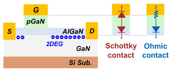
Figure 1.
Schematics of the GaN HEMT device and gate structures.
Pulsed transfer characteristic tests with prolonged negative quiescent gate bias (VGSQ) were carried out under a Keithley 4200-SCS system with ultrafast I-V modules (4225-PMU). As shown in Figure 2, to minimize the extra charge accumulation introduced by the measurement [13], the pulse width (tm) of each test point was fixed at 10 μs, and the gate voltage scanning range was limited from 0 V to 3 V. The voltage step was 0.03 V, and 100 test points were adopted in each pulsed transfer measurement. Meanwhile, the pulse period was much longer, and it was set to no less than 1 ms, corresponding to a duty ratio of 1% or less. In addition, a time interval of 300 s was adopted between the adjacent pulsed transfer measurements to ensure a full recovery of VT before each measurement.

Figure 2.
Schematics of a pulsed transfer characteristic test with negative quiescent gate bias (VGSQ).
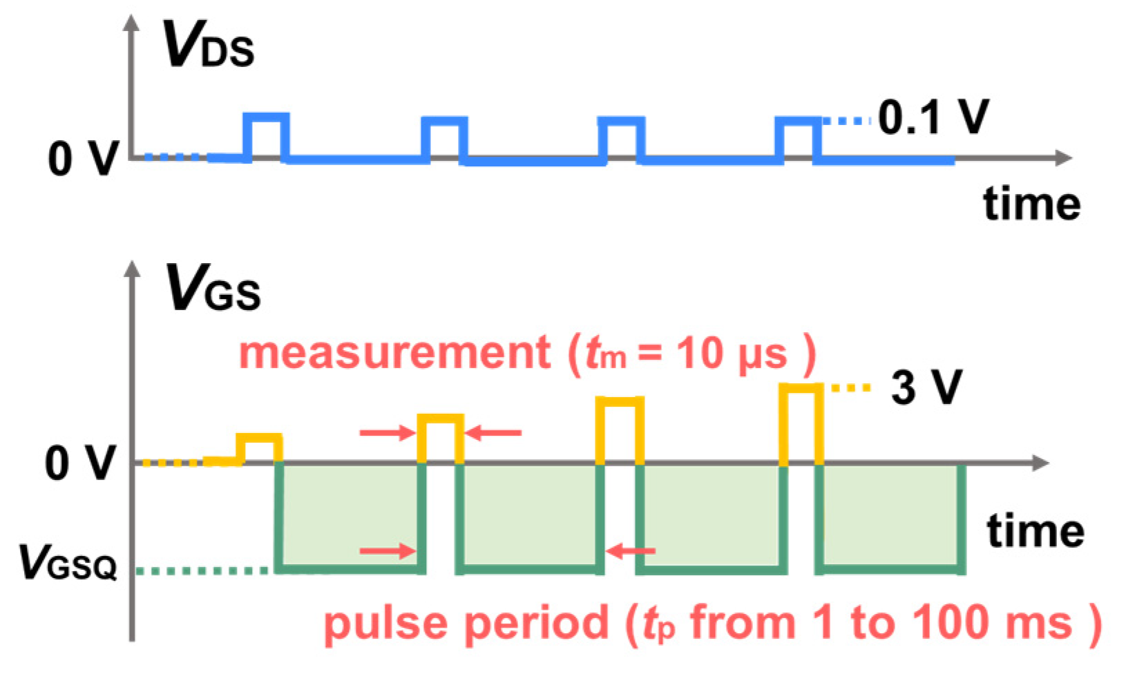
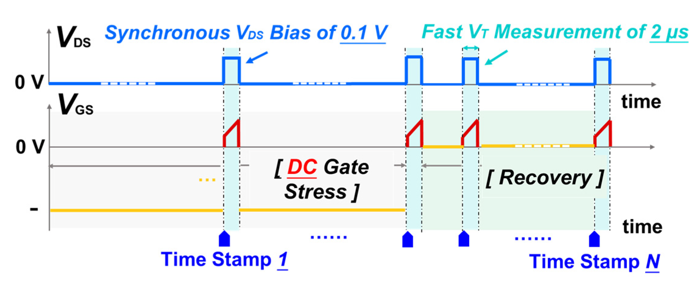
Although the prolonged pulse test method could roughly reflect the impact of negative gate bias stress and the stress duration on device VT stability, it still lacks transient VT shift (ΔVT) details in the stress and recovery processes. Thus, a series of MSM sequences with a −µs level of periodically inserted ID-VG measurements were conducted to further explore the transient details, as shown in Figure 3. To minimize the testing error induced by extra charge accumulation, low forward gate sweeping voltages, from 1 V to 3 V and 0 V to 2 V, were applied on SG and OG HEMTs, respectively, in a short testing time of 2 µs. The influence of the sweeping measurements has been carefully pre-evaluated through without-stress monitory tests. In addition, a DC gate bias, varying from −4 V to −10 V, was adopted in the stress process, followed by a 1000 s recovery process with zero gate bias. Furthermore, the temperature-dependent transient ΔVT, from room temperature to 150 °C, was also evaluated under negative gate bias stress.
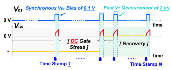
Figure 3.
Schematics of an MSM sequence for transient ΔVT characterization in stress and recovery processes under negative DC gate stress.
3. Results and Discussion
3.1. VT Shift in Pulse Transfer Tests
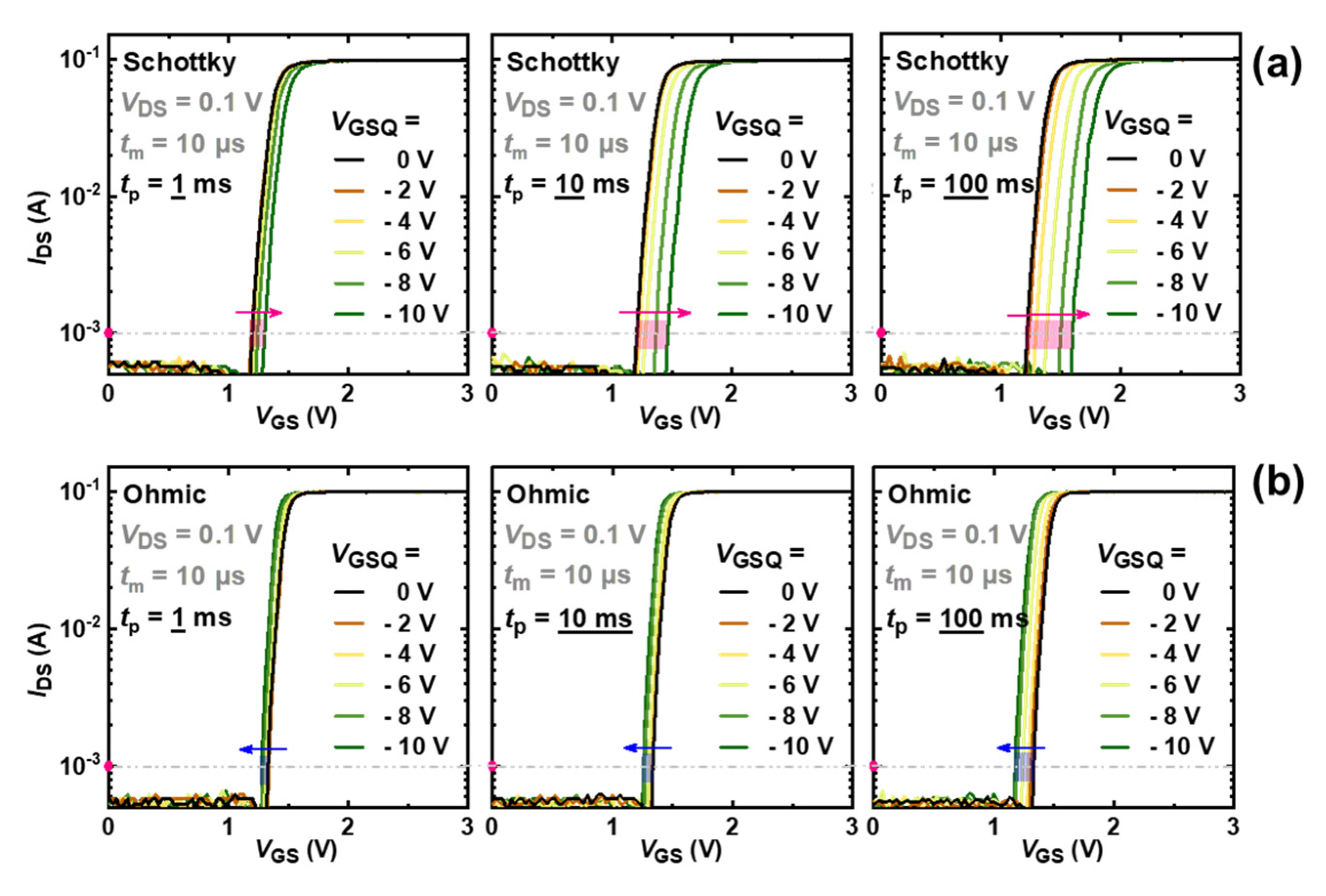
As shown in Figure 4, the VT shift of both two types of devices increases with increasing pulse stress time and negative gate stress bias, but their shift directions are opposite. For SG devices, VT under tp = 100 ms shows a forward shift, from approximately 1.2 V to 1.6 V, when VGSQ varies from 0 V to −10 V, as shown in Figure 4a. In contrast, a smaller backward VT shift, from around 1.30 to 1.25, is observed for OG devices under the same test conditions, as shown in Figure 4b. The different VT shift behaviors indicate different extra charge accumulations in the gate region, and the detailed physical mechanism for this discrepancy will be further investigated by a series of MSM sequences.
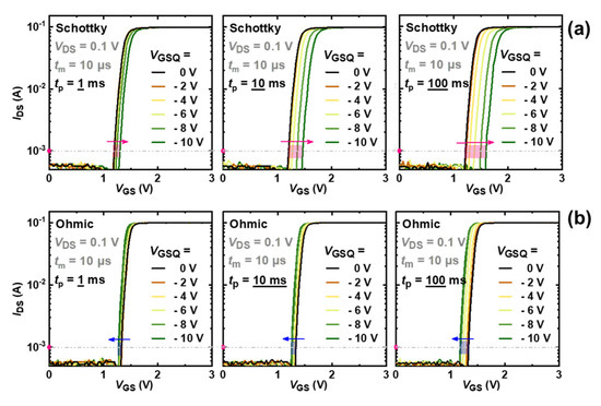
Figure 4.
Pulsed transfer characteristic curves with VGSQ, from 0 V to −10 V, and pulse periods of 1 ms, 10 ms, and 100 ms: (a) SG HEMT, (b) OG HEMT.
3.2. Transient ΔVT Evolution in MSM Sequences
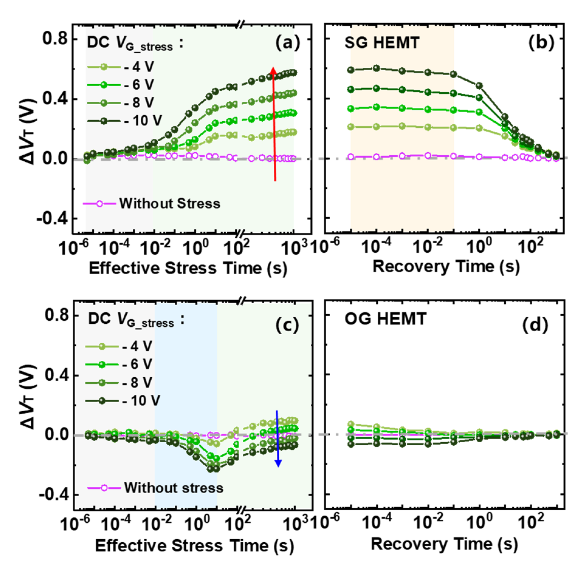
As shown in Figure 5, the transient ΔVT of SG HEMTs shows no obvious change during the initial stress process (5 µs–10 ms). As the stress time continues, ΔVT begins to increase and becomes gradually saturated with a further increase in stress time. It is also worth mentioning that ΔVT becomes more positive with increasing negative gate bias stress, as marked by the red arrow in Figure 5a. During the recovery process, as shown in Figure 5b, ΔVT remains almost unchanged for the initial 0.1 s, and then, it can gradually recover to the initial state in the subsequent 1000 s. Compared with SG HEMTs, OG HEMTs feature a smaller amplitude in ΔVT under the same stress conditions. In addition, ΔVT shows non-monotonic change as the stress time increases. More specifically, ΔVT first drops to a negative value, after approximately 1 s of stress time, as marked by the blue shade in Figure 5c. After that, ΔVT gradually rises to a stable state. Besides, the change trend of ΔVT, with the gate bias stress in OG HEMTs, is opposite to that in SG HEMTs, as marked by the blue arrow in Figure 5c. In the subsequent recovery process, OG HEMTs demonstrate a faster recovery speed, where VT starts the recovery process immediately after the removal of gate bias stress and can fully recover to the initial state in approximately 1 s recovery time.

Figure 5.
Transient ΔVT evolution in 1000 s stress and subsequent 1000 s recovery processes, with gate stress from −4 V to −10 V, under room temperature: (a,b) SG HEMT, (c,d) OG HEMT.
However, the ΔVT evolution, with stress and recovery time, at elevated temperatures is found to be very different from the behavior at room temperature, for both SG and OG HEMTs, when conducting negative bias stress MSM sequences. As shown in Figure 6, ΔVT, with stress time in SG HEMTs, features a concave-shaped evolution process under the given negative bias stress, and the concave shape occurs earlier and features a larger amplitude with the increasing temperature. It is very interesting that a convex-shaped VT evolution appears, correspondingly, in the recovery process. In addition, as marked by the black arrows, the final saturated ΔVT decreases with the increasing temperature under the given gate bias stress.
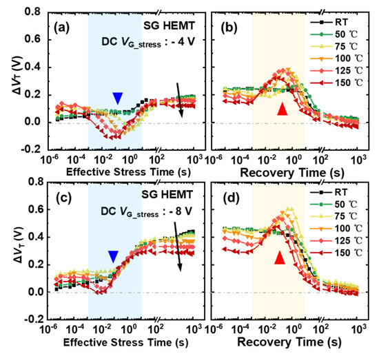
Figure 6.
ΔVT evolution of SG HEMT in 1000 s stress and subsequent 1000 s recovery processes under elevated temperature, with gate bias stress at: (a,b) −4 V and (c,d) −8 V.
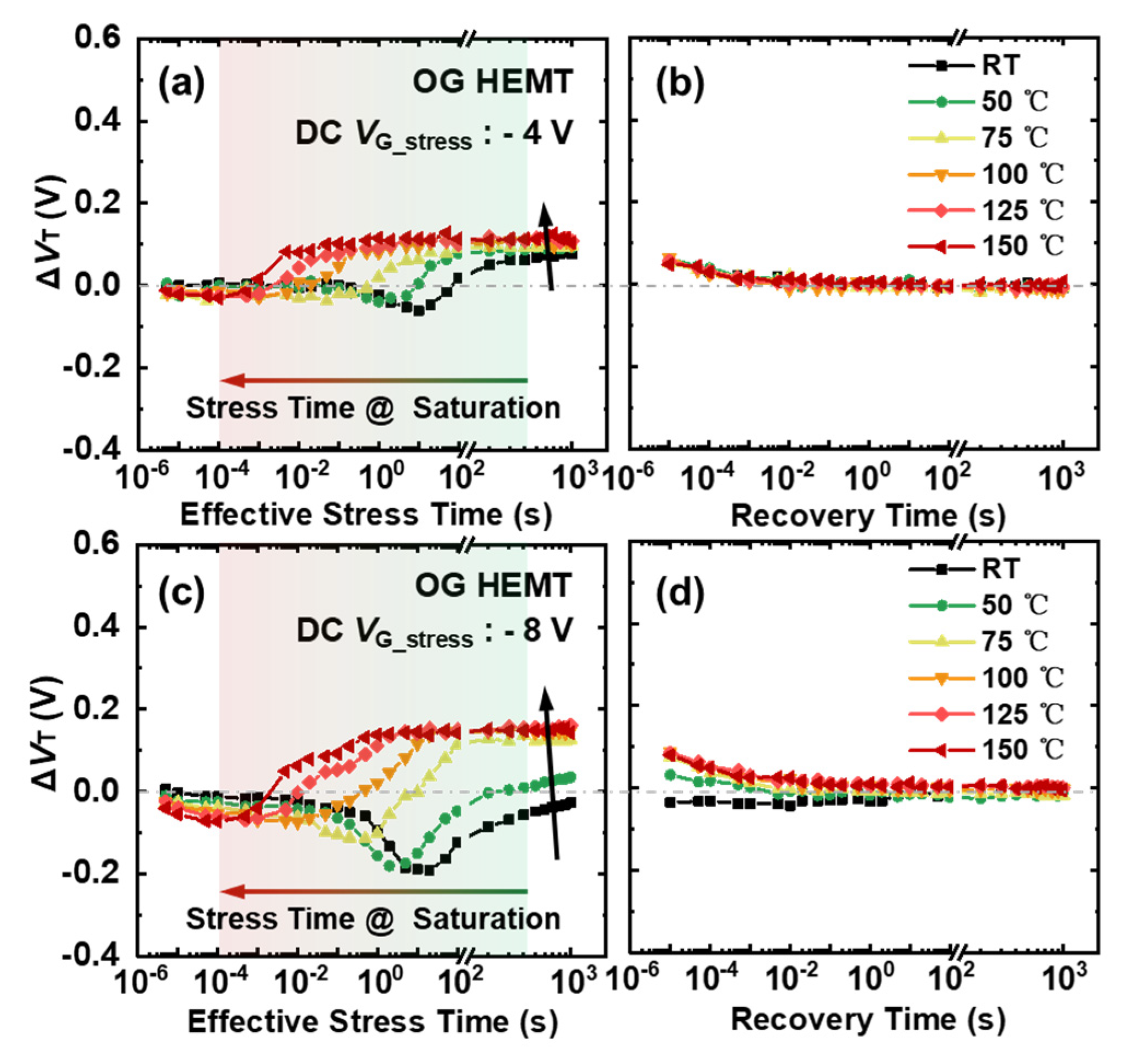
For OG HEMTs, the change in ΔVT is generally smaller in comparison with SG HEMTs. As shown in Figure 7a–c, ΔVT becomes slightly more negative in the initial stress process and, then, begins to rise to a stable and positive value earlier, with the increasing temperature, for all the given gate bias stress. The time to reach the stable state for ΔVT is greatly shortened from 100 s to 1 ms when the temperature varies from room temperature to 150 °C. In addition, this stable ΔVT seems to grow gradually saturated with further increases in temperature. The recovery process becomes simpler with a quick and monotonous change to the initial state.
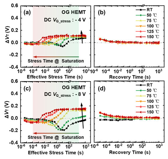
Figure 7.
ΔVT evolution of OG HEMT in 1000 s stress and subsequent 1000 s recovery processes, under elevated temperature, with gate bias stress at: (a,b) −4 V and (c,d) −8 V.
3.3. Physical Mechanism Analysis
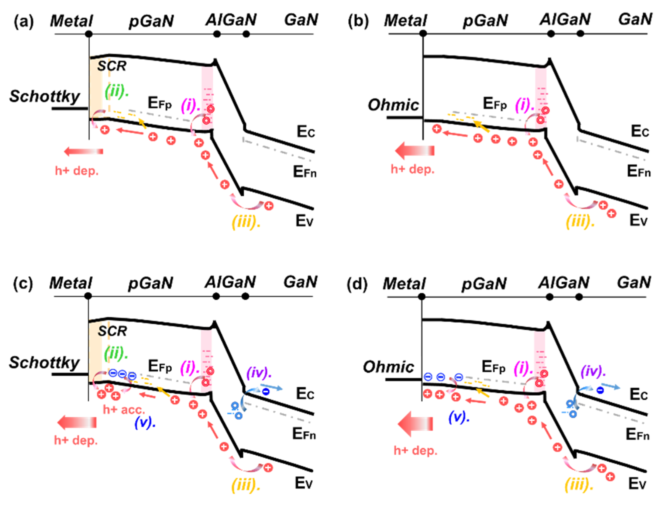
The transient ΔVT evolution of devices during stress and subsequent recovery processes, presented above, reflects the dynamic changes of net charges underneath the gate stack region. Figure 8 illustrates the schematic energy band diagram of the device gate stack region under negative gate bias stress. Under the stress condition, the p-GaN/AlGaN/GaN heterojunction is reverse biased, and a depletion region takes place, as marked by the red shadow. In particular, the metal/p-GaN Schottky junction in SG HEMTs is forward biased, and it features an additional Space Charge Region (SCR) compared to that in OG HEMTs, as marked by the yellow shadow.
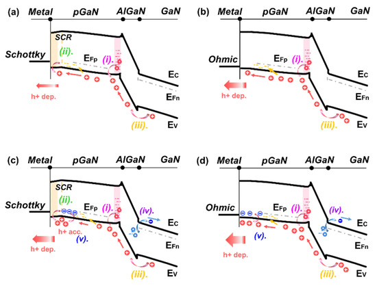
Figure 8.
Schematic band diagrams of the gate stack region in the negative gate stress process under room temperature: (a) SG HEMT, (b) OG HEMT; under elevated temperature: (c) SG HEMT, (d) OG HEMT.
At room temperature, little electron injection or a trapping process could be introduced under the negative gate bias stress [18], while the depletion or accumulation of holes plays a major role and is further investigated. The positive ΔVT during the gate stress process could stem from the hole emission of the gate-stack region of p-GaN gate HEMTs, which is equivalent to the depletion of net positive charges. In contrast, the negative ΔVT results from hole accumulation. The behavior of ΔVT could be linked to three physical processes, as illustrated in Figure 8a,b:
- Donor-type hole trap states at the p-GaN/AlGaN interface could be activated and release holes to the valence band in the p-GaN layer [17,18];
- The depletion width of SCR, in the p-GaN layer of SG HEMTs, would decrease under the negative gate bias stress, which also leads to hole release [4];
- Holes could flow from the gate-source drift region, towards the gate stack, and under large negative gate bias stress. Part of the holes may flow out to the gate terminal and contribute to the gate current, while part of the holes may get trapped into the gate stack region and lead to an extra hole accumulation [16].
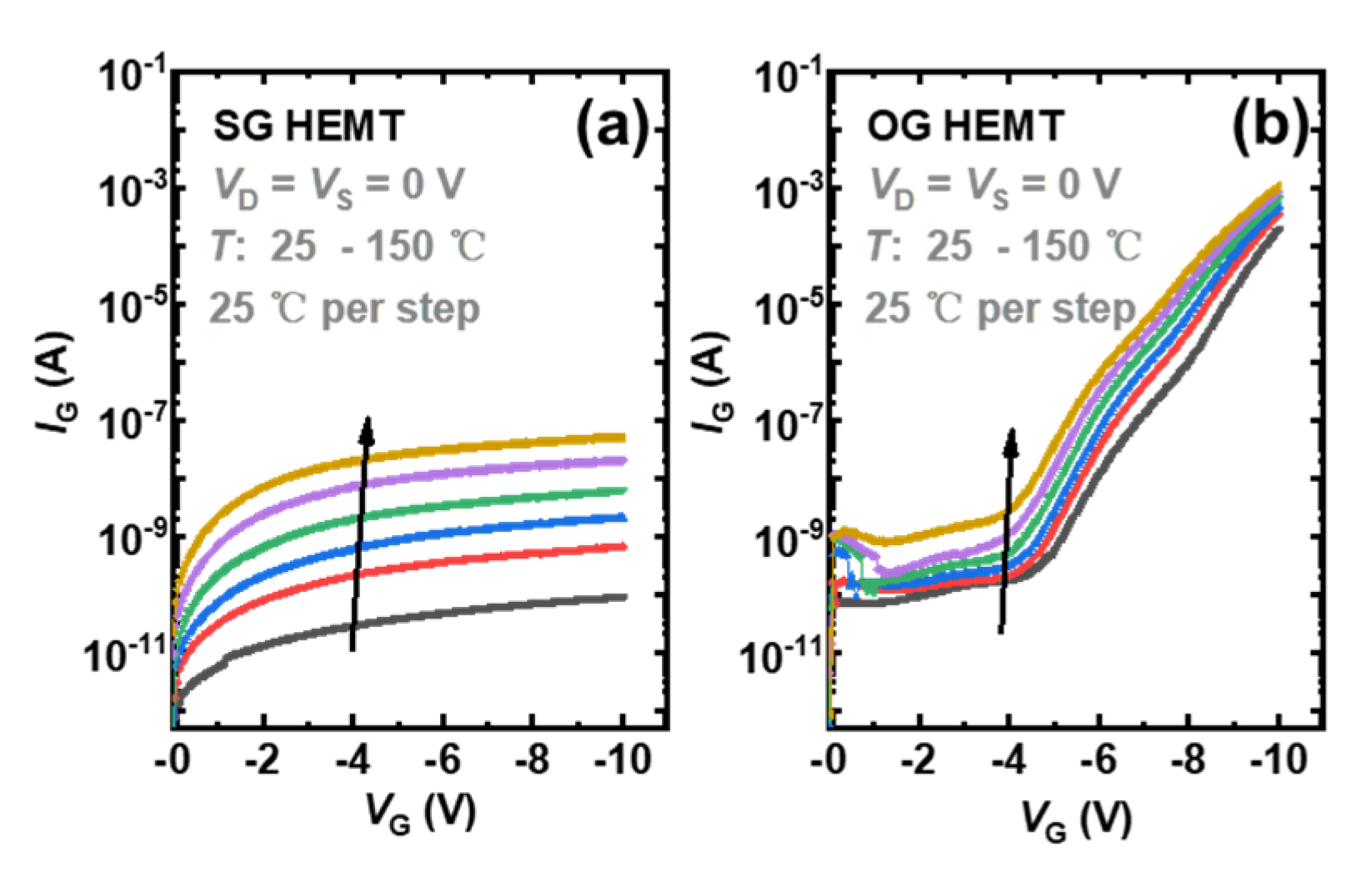
In SG HEMTs, the increase in the saturated ΔVT, with increasing negative bias stress in Figure 5a, corresponds to further depletion of holes. With the increasing electric field under higher bias stress, more holes released in process (i)–(iii) could be emitted to gate metal and drift away, leading to a higher extent of hole deficiency. In contrast, OG HEMTs exhibit a smaller VT shift toward the opposite direction with increasing negative bias stress, as shown in Figure 5c. For OG HEMTs, holes would be less released through process (ii) because of the absence of the SCR. In addition, the p-i-n diode mainly undertakes the reverse-bias voltage, and the electric field drop across the AlGaN barrier is larger in OG HEMTs, compared with that in SG HEMTs, under given negative gate stress. Thus, it is easier for a hole to cross the AlGaN barrier layer and inject into the gate stack region in OG HEMT. Besides, with an increasing negative bias, OG HEMTs feature a larger gate leakage current, which is six orders of magnitude higher than that in SG HEMTs, under a given gate bias of −10 V, as shown in Figure 9. The increased difference in the gate leakage current, under large reverse gate bias, indicates that the process (iii) plays an important role in OG HEMTs. As a result, hole accumulation gradually becomes dominated in the gate stack region of OG HEMTs, as negative gate bias stress increases and, hence, leads to a more negative ΔVT. Moreover, in the subsequent recovery processes, SG HEMTs demonstrate a slower recovery process compared to OG HEMTs Figure 5b,d. This phenomenon could be attributed to the presence of the Schottky barrier at the metal/p-GaN junction in SG HEMTs. Different from OG HEMTs, the p-GaN bulk begins electrically floating with the formation of Schottky-type contacts at the metal/p-GaN interface in SG HEMTs. When the stress is withdrawn, the previously reduced SCR depletion width in the p-GaN layer of SG HEMTs is restored, and the valance–band offset at the metal/p-GaN junction increases and returns to the original state. This Schottky barrier will hinder the backflow of those holes depleted in the stress phase and, hence, results in a slower recovery process in SG HEMTs.
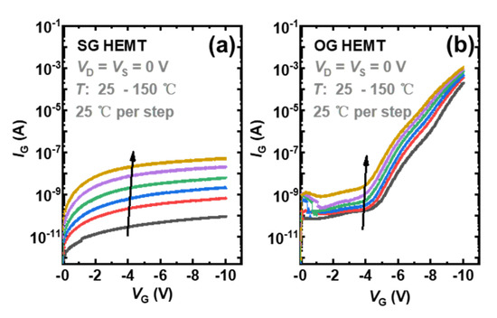
Figure 9.
Gate leakage current of p-GaN gate devices under various temperatures: (a) SG HEMT, (b) OG HEMT.
In principle, both hole injection or release in processes (i)–(iii) could be enhanced through thermal assistance under elevated temperatures. Additionally, more detailed physical processes should be taken into consideration, as shown in Figure 8c,d:
- The deep-level defects in the AlGaN layer could be activated with an increasing temperature and participate in the de-trapping process of electrons at the negative gate bias;
- The acceptors in the p-GaN cap layer could be quickly ionized with an increasing temperature and, hence, release holes at the negative gate bias, leaving net negative charges behind.
As a result, the distinct transient ΔVT behavior, under the elevated temperature for two types of devices, could be attributed to a combination of the above processes. For SG HEMTs, the concave-shaped ΔVT evolution, in the range of around 10 ms to 1 s stress time, could be linked to a temporary accumulation of net positive charges during the initial stress stage. For one thing, the electrons released by the activated deep-level defects, through the process (iv), are driven away from the gate stack region under the electric field. Meanwhile, more holes could also be released through processes (v) with increasing temperatures, and these extra released holes could not fully drift away in short time, due to the block of Schottky barrier. Consequently, the more obvious concave-shaped ΔVT evolution occurs with increasing temperatures.
In addition, the convex-shaped ΔVT evolution in the recovery process is also associated with the involvement of process (iv). When the bias stress is withdrawn, the electrons driven away during the stress process gradually flow back to the gate stack region. However, the holes could not be replenished immediately, due to the blocking of the Schottky barrier. For these reasons, negative net charge accumulation becomes temporarily dominated, and hence, convex-shaped ΔVT evolution occurs in the recovery process. As recovery time increases, the number of electrons re-captured by the deep-level defects becomes saturated. The transient ΔVT could recover to the initial state as the reduced positive charges are gradually restored. Moreover, the reduction in the saturated ΔVT with an increasing temperature could be ascribed to the participation of processes (v). With the increasing ionization of acceptors under elevated temperatures, more net negative charges are left behind and could balance the voltage drop on the gate stack region, hence resulting in a reduction in the saturated ΔVT under the given gate bias stress.
For OG HEMTs, the concave-shaped VT evolution that occurred at room temperature gradually disappears, and the time of reaching the saturated ΔVT becomes shorter with the increasing temperature under the given gate bias stress. These phenomena indicate an accelerated hole depletion process underneath the gate stack region. With lower barrier height in OG HEMTs, more holes under elevated temperatures could be emitted to the gate metal and drift away. In addition, the recovery process in OG HEMTs is simpler and exhibits quick and monotonic change towards the initial state, which could also be attributed to the flowing of holes back under the low barrier being easier.
4. Conclusions
In summary, the temperature-dependent transient ΔVT evolution in OG and SG HEMTs, under negative gate bias stress, are captured in the −μs to −ks time window by fast sweeping characterizations, and some interesting phenomena are observed. As the temperature increases, SG HEMTs exhibit distinct concave-shaped and convex-shaped ΔVT evolution in the stress and recovery processes, separately, while OG HEMTs exhibit an accelerated ΔVT increase, towards the positive direction, in the stress process and monotonic change in the recovery process. These transient details reflect the dynamic net charge variations underneath the gate stack region, and the time and temperature-dependent hole trapping, releasing, and transport processes are further analyzed through the proposed physical mechanisms. The comprehensive mechanism analysis takes account of the differences in device structures, as well as the participation of different physical processes under elevated temperatures, which contributes to a better understanding on the characteristics of p-GaN gate HEMTs.
Author Contributions
Methodology, R.W.; investigation, R.W.; validation, H.G., Q.H., J.L., J.X. and J.W.; writing—original draft preparation, R.W.; writing—review and editing, D.C.; supervision, B.L., H.L., R.Z. and Y.Z.; funding acquisition, D.C., J.L. and J.W. All authors have read and agreed to the published version of the manuscript.
Funding
This work was funded by the National Natural Science Foundation of China (61634002, 62104096, and 62104110), NSAF (U1830109) and the State Key R&D project of Jiangsu (BE2021026).
Conflicts of Interest
The authors declare no conflict of interest.
References
- Chen, K.J.; Haberlen, O.; Lidow, A.; Tsai, C.l.; Ueda, T.; Uemoto, Y.; Wu, Y. GaN-on-Si Power Technology: Devices and Applications. IEEE Trans. Electron Devices 2017, 64, 779–795. [Google Scholar] [CrossRef]
- Amano, H.; Baines, Y.; Beam, E.; Borga, M.; Bouchet, T.; Chalker, P.R.; Charles, M.; Chen, K.J.; Chowdhury, N.; Chu, R.; et al. The 2018 GaN power electronics roadmap. J. Phys. D Appl. Phys. 2018, 51, 163001. [Google Scholar] [CrossRef]
- Ma, C.-T.; Gu, Z.-H. Review of GaN HEMT Applications in Power Converters over 500 W. Electronics 2019, 8, 1401. [Google Scholar] [CrossRef] [Green Version]
- Wang, H.; Wei, J.; Xie, R.; Liu, C.; Tang, G.; Chen, K.J. Maximizing the Performance of 650-V p-GaN Gate HEMTs: Dynamic RON Characterization and Circuit Design Considerations. IEEE Trans. Power Electron. 2017, 32, 5539–5549. [Google Scholar] [CrossRef]
- Del Alamo, J.A.; Lee, E.S. Stability and Reliability of Lateral GaN Power Field-Effect Transistors. IEEE Trans. Electron Devices 2019, 66, 4578–4590. [Google Scholar] [CrossRef]
- Ruzzarin, M.; Meneghini, M.; Barbato, A.; Padovan, V.; Haeberlen, O.; Silvestri, M.; Detzel, T.; Meneghesso, G.; Zanoni, E. Degradation Mechanisms of GaN HEMTs With p-Type Gate Under Forward Gate Bias Overstress. IEEE Trans. Electron Devices 2018, 65, 2778–2783. [Google Scholar] [CrossRef]
- Sayadi, L.; Iannaccone, G.; Sicre, S.; Haberlen, O.; Curatola, G. Threshold Voltage Instability in p-GaN Gate AlGaN/GaN HFETs. IEEE Trans. Electron Devices 2018, 65, 2454–2460. [Google Scholar] [CrossRef]
- He, J.B.; Tang, G.F.; Chen, K.J. V-TH Instability of p-GaN Gate HEMTs Under Static and Dynamic Gate Stress. IEEE Electron Device Lett. 2018, 39, 1576–1579. [Google Scholar]
- Tang, X.; Li, B.K.; Moghadam, H.A.; Tanner, P.; Han, J.S.; Dimitrijev, S. Mechanism of Threshold Voltage Shift in p-GaN Gate AlGaN/GaN Transistors. IEEE Electron Device Lett. 2018, 39, 1145–1148. [Google Scholar] [CrossRef]
- Shi, Y.Y.; Zhou, Q.; Cheng, Q.; Wei, P.C.; Zhu, L.Y.; Wei, D.; Zhang, A.B.; Chen, W.J.; Zhang, B. Carrier Transport Mechanisms Underlying the Bidirectional V-TH Shift in p-GaN Gate HEMTs Under Forward Gate Stress. IEEE Trans. Electron Devices 2019, 66, 876–882. [Google Scholar] [CrossRef]
- Li, B.K.; Li, H.; Wang, J.N.; Tang, X. Asymmetric Bipolar Injection in a Schottky-Metal/p-GaN/AlGaN/GaN Device Under Forward Bias. IEEE Electron Device Lett. 2019, 40, 1389–1392. [Google Scholar] [CrossRef]
- Li, X.; Bakeroot, B.; Wu, Z.; Amirifar, N.; You, S.; Posthuma, N.; Zhao, M.; Liang, H.; Groeseneken, G.; Decoutere, S. Observation of Dynamic V-TH of p-GaN Gate HEMTs by Fast Sweeping Characterization. IEEE Electron Device Lett. 2020, 41, 577–580. [Google Scholar] [CrossRef]
- Wang, R.; Lei, J.M.; Guo, H.; Li, R.; Chen, D.J.; Lu, H.; Zhang, R.; Zheng, Y.D. V-T Shift and Recovery Mechanisms of p-GaN Gate HEMTs Under DC/AC Gate Stress Investigated by Fast Sweeping Characterization. IEEE Electron Device Lett. 2021, 42, 1508–1511. [Google Scholar] [CrossRef]
- Chen, X.; Zhong, Y.; Zhou, Y.; Su, S.; Yan, S.; Guo, X.; Gao, H.; Zhan, X.; Ouyang, S.; Zhang, Z.; et al. Influence of the carrier behaviors in p-GaN gate on the threshold voltage instability in the normally off high electron mobility transistor. Appl. Phys. Lett. 2021, 119, 063501. [Google Scholar] [CrossRef]
- Li, X.; Posthuma, N.; Bakeroot, B.; Liang, H.; You, S.; Wu, Z.; Zhao, M.; Groeseneken, G.; Decoutere, S. Investigating the Current Collapse Mechanisms of p-GaN Gate HEMTs by Different Passivation Dielectrics. IEEE Tran. Power Electron. 2021, 36, 4927–4930. [Google Scholar] [CrossRef]
- Oeder, T.; Pfost, M. Gate-Induced Threshold Voltage Instabilities in p-Gate GaN HEMTs. IEEE Trans. Electron Devices 2021, 68, 4322–4328. [Google Scholar] [CrossRef]
- Elangovan, S.; Chang, E.Y.; Cheng, S. Analysis of Instability Behavior and Mechanism of E-Mode GaN Power HEMT with p-GaN Gate under Off-State Gate Bias Stress. Energies 2021, 14, 2170. [Google Scholar] [CrossRef]
- Zhang, C.; Liu, S.; Li, S.; Li, N.; Tao, X.; Hou, B.; Zhou, B.; Wei, J.; Chen, Y.; Sun, W. Electrical performances degradations and physics based mechanisms under negative bias temperature instability stress for p-GaN gate high electron mobility transistors. Semicond. Sci. Technol. 2021, 36, 014007. [Google Scholar] [CrossRef]
- Murukesan, K.; Efthymiou, L.; Udrea, F. On the Challenges of Reliable Threshold Voltage Measurement in Ohmic and Schottky Gate p-GaN HEMTs. IEEE J. Electron Devices Soc. 2021, 9, 831–838. [Google Scholar] [CrossRef]
- Roschatt, P.M.; Pickering, S.; McMahon, R.A. Bootstrap Voltage and Dead Time Behavior in GaN DC-DC Buck Converter with a Negative Gate Voltage. IEEE Trans. Power Electron. 2016, 31, 7161–7170. [Google Scholar] [CrossRef]
- GaN Systems. GN012 Gate Driver Design with GaN E-HEMTs Application Note. 2022. Available online: http://www.gansystems.com (accessed on 30 May 2022).
- Infineon. Driving CoolGaN™ 600 V High Electron Mobility Transistors Application Note. 2022. Available online: https://www.infineon.com (accessed on 30 May 2022).
- GaN Systems. GS66502B Datasheet. 2022. Available online: http://www.gansystems.com (accessed on 30 May 2022).
- Infineon. IGT60R190D Datasheet. 2021. Available online: https://www.infineon.com (accessed on 30 May 2022).


Publisher’s Note: MDPI stays neutral with regard to jurisdictional claims in published maps and institutional affiliations. |
© 2022 by the authors. Licensee MDPI, Basel, Switzerland. This article is an open access article distributed under the terms and conditions of the Creative Commons Attribution (CC BY) license (https://creativecommons.org/licenses/by/4.0/).