Abstract
In this paper, a 650 V 4H-SiC trench Metal-Oxide-Semiconductor Field-Effect Transistor (MOSFET) with a hetero-junction diode (HJD) and double current spreading layers (CSLs) is proposed and studied based on Sentaurus TCAD simulation. The HJD suppresses the turn-on of the parasitic body diode and improves the performance in the third quadrant. CSLs with different doping concentrations help to lower the on-state resistance as well as the gate-drain capacitance. As a result, the on-state resistance is decreased by 47.82% while the breakdown voltage remains the same and the turn-on and turn-off losses of the proposed structure are reduced by 83.39% and 68.18% respectively, compared to the conventional structure.
1. Introduction
Silicon carbide (SiC), as known as wide band-gap semiconductors, is widely used in power devices such as MOSFET, providing lower on-state resistance (Ron), higher breakdown voltage (BV), and better frequency characteristics [1,2,3,4]. However, the body diode of SiC MOSFETs has a higher turn-on voltage compared with Si MOSFETs, leading to higher switching loss and causing the inherent bipolar degradation effect [5]. Moreover, due to the basal plane dislocations (BPDs), the long-term reliability of the device is a concern [6].
To solve the problem of the body diode, many works of literature have been published. Schottky Barrier Diodes (SBDs) are widely used to replace the body diode working as reverse diodes in SiC MOSFETS, such as the SiC MOSFET with the merged junction barrier controlled Schottky rectifier, the SiC MOSFET with the built-in SBD and the SiC split-gate MOSFET with merged SBD [7,8,9]. While SBDs can optimize the recovering characteristics, they can consume a large part of the active chip area, and lead to high leakage current.
A SiC MOSFET with a MOS-Channel diode is another solution raised recently, but a strong electric field at the edge of the dummy gate may cause reliability issues [10,11,12].
Now heterojunction diode (HJD) has become a new option. HJD formed between poly-silicon and 4H-SiC presents similar characteristics as SBD [13], but needs less area for chips. Several structures have been proposed [14,15,16]. A split-gate SiC trench MOSFET with a P-poly/SiC hetero-junction diode has been proposed for optimized reverse recovery characteristics and low switching loss [17]. Furthermore, SiC MOSFET with integrated n-/n-type poly-Si/SiC heterojunction freewheeling diode has been proposed, offering a lower Vf, but at the cost of BV [18].
In this paper, a new 650 V SiC trench MOSFET with an embedded heterojunction diode is proposed and studied with numerical simulation. The novel structure is compared with the conventional asymmetric channel SiC trench MOSFET (C-MOS). Simulation has shown that the conventional structure has excellent temperature stability and gate oxide reliability but did not concern the problem of the body diode; therefore, a heterojunction diode is embedded into the proposed structure, which prominently improves the recovering characteristics and switching loss. Furthermore, to improve the on-state performance, CSLs attached with a shallow trench gate are introduced as well [19].
2. Device Structure
Figure 1a,b show the cross-sectional views of the C-MOS and the proposed structure. Compared with the C-MOS, the proposed structure has a P+ doped poly-Si, a deep P+ well surrounding the p-base, and a shallow poly-silicon gate trench as well as CSLs of different doping concentrations. The P+ poly-Si is connected to the source metal, forming an HJD with n-4H-SiC.
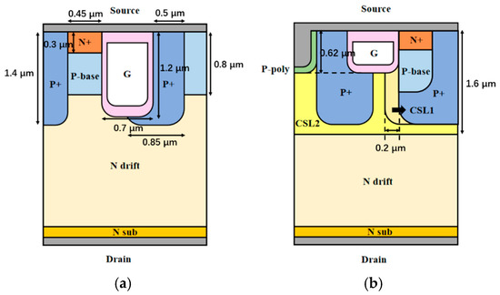
Figure 1.
Cross-sectional views of (a) C-MOS and (b) proposed structure.
The p-poly and the CSL2 form the HJD. Figure 2 shows the energy band diagram of P-poly/N-SiC heterojunction diode. The thickness of the poly-Si is 0.12 μm horizontally and 0.06 μm vertically. The doping concentration is 1 × 1020 cm−3. The energy gaps in the HJD for conduction and valence bands are 0.44 eV and 1.82 eV, respectively, providing unipolar action like SBD. The barrier height ΦBN is about 1.48 eV. When the forward bias was applied, the built-in potential began decreasing, and the conduction band of the CSL2 rises, causing the electrons in the CSL2 to easily migrate to the P-poly region, but the high energy barrier prevents the holes from passing from CSL2 to the P-poly, providing a low forward voltage (Vf) while keeping the breakdown voltage high.
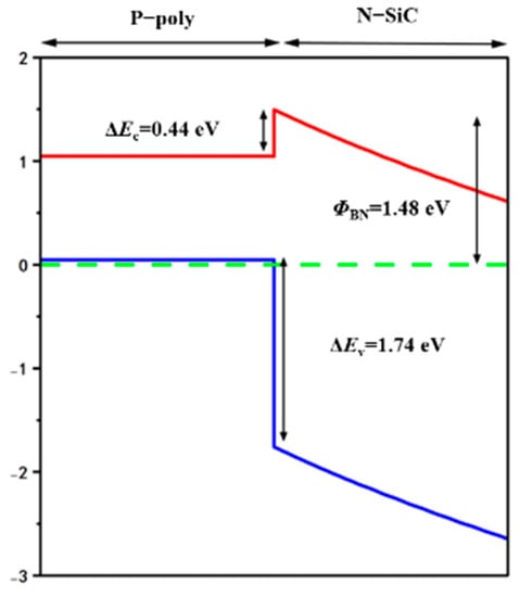
Figure 2.
Band diagram of P-poly/N-SiC heterojunction diode.
The gate depths of the C-MOS and the HJD-TMOS are 0.62 μm and 1.2 μm respectively. Since the shallow trench gate enlarges the Junction Field-Effect Transistor (JFET) area and reduces the peak electric field and the Crss, an over-short channel length will lead to high leakage current and even breakdown of the BV. So, the shallow trench gate of the HJD-MOS is set to 0.62 μm. The thicknesses of the gate oxide layer in the wall and bottom are 60 and 120 nm, respectively.
The deep P+ well surrounding the p-base was set to deplete the CSL, providing a strong pinch-off effect to lower the leaking current and guarantee the BV. The C-MOS and the proposed HJD-TMOS have the same doping concentration and closed device dimensions. The depth of the P+ well is 1.4 μm, and the depth of the P-base is 0.8 μm. The depth of the CSL1 is the same as the deep P+ well, and its thickness is 0.2 μm. The doping concentration of the CSL1 is 5 × 1017 cm−3. The depth of the CSL2 is 1.6 μm and its doping concentration is 2 × 1016 cm−3. The other parameters of the two structures are summarized in Table 1.

Table 1.
Parameters of C-MOS and Proposed HJD-MOS.
For device simulations, Sentaurus TCAD (Synopsys Inc., CA, USA) is used to reveal the electric characteristics. SRH, AUGER, and OkutoCrowwell are used as models to describe trap-assisted recombination [20,21,22], the non-radiative process involving three carriers, and the breakdown analysis, respectively. The temperature is set to 300 K.
3. Simulation Results and Discussions
Figure 3 shows the influence of different widths of CSL1 (Wc1) on BV, on-state resistance, and switching loss of the structure. When the Wc1 rises, the BV and Ron both decrease, but the switching loss of the structure decreases first, reaches the bottom when Wc1 is 200 nm, and rises afterward. When Wc1 is less than 200 nm, the majority carriers of the JFET area are holes, and with the increase in Wc1, the concentration of electrons also rises. When Wc1 reaches 200 nm, the JFET area is depleted, and the Qgd reaches its lowest value, minimizing the switching loss value as well. When Wc1 rises, the majority carriers change into electrons, and the switching loss rises again. Moreover, the decrease in the Ron is gradually smooth when Wc1 increases to 200 nm, since a further increase in Wc1 does not help to widen the current path. Therefore, the Wc1 is set as 200 nm in the structure.
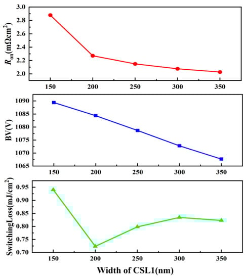
Figure 3.
The influence of the width of CSL1 (Wc1) on the Ron (VGS = 15 V), BV (VGS = 0 V) and switching loss.
Figure 4 shows the electric field distributions of C-MOS and the proposed structure in the off state when the VDS is 650 V. According to research [23], the maximum oxide electric field (EMOX) to obtain a lifetime of more than 10 years was estimated to be 2.7 MV·cm−1 in blocking state. Because of the deep P+ shielding layer, both of the structures have a lower electric field than 2.7 MV·cm−1 at the gate oxide. Since the proposed structure has shallower gate oxide, when the source is biased zero, and the drain is applied with large bias voltage, the P+ shielding region can deplete the CSLs, preventing the high drain electric field from affecting the trench gate, so the peak electric field around the trench gate corner is also lower than the C-MOS, which means it has higher gate reliability. As in the corner of the P+ well, the two structures have similar peak electric fields.
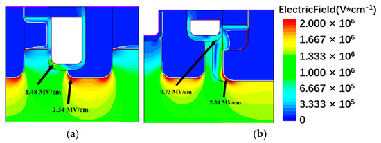
Figure 4.
The electric field distribution of (a) C-MOS, (b) proposed structure.
Figure 5 shows the first quadrant I-V characteristics of the C-MOS and the proposed structure. The voltage of the gate (Vgs) is 15 V. The Ron, sp of the proposed structure is 47.82% lower than the C-MOS. The CSLs provide a better depletion area at the JFET region. Figure 5b,c show the current path of the two structures, the width of the proposed structure is wider than the C-MOS, making a lower on-state resistance. At the same time, the saturation current of the proposed structure is lower than the C-MOS, providing a better short-circuit capability.
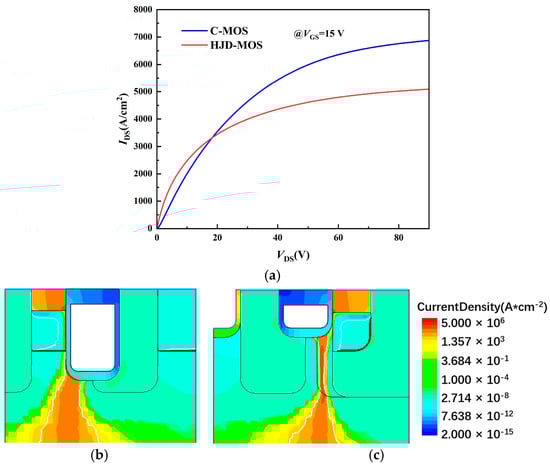
Figure 5.
The (a) first quadrant I-V characteristics of the C-MOS and the proposed structure and the current path of (b) C-MOS and (c) proposed structure.
Figure 6 shows the reverse characteristics when Vgs is set to −5 V. The turn-on voltage (Vf) of the HJD is 1.2 V compared to 2.8 V of the body diode, leading to a remarkable reduction in dead-time loss.
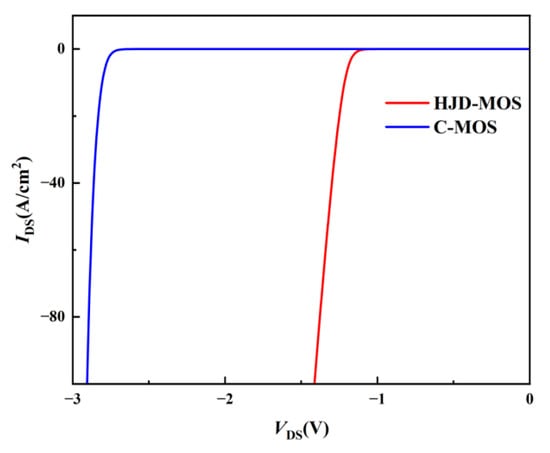
Figure 6.
The reverse characters of the C-MOS and the proposed structure.
As shown in Figure 7a,b, in the proposed structure, the reverse current goes through HJD rather than through body diode as the C-MOS, which avoids the inherent bipolar degradation effect and the BPDs.
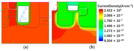
Figure 7.
The current distribution of (a) C-MOS and (b) proposed structure.
Figure 8 compares the off-state characteristics of the two structures. The BV of the proposed structure and the C-MOS are 1084 V and 1043 V respectively. The doping concentration of the CSL is much lower than the deep P+ regions, making it easily depleted at high drain voltage. The shallow gate trench leads to a higher JFET resistance, creating a balance between Ron and BV. Although the wider current path may lead to a higher leak current in off-state conditions, the strong pinch-off effect provided by deep P+ well helps to offset the problem.
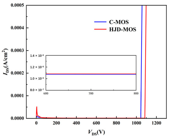
Figure 8.
The off-state characteristics of the C-MOS and the proposed structure.
Figure 9 shows the gate charges of the two devices. The proposed structure has a much lower miller plateau than the C-MOS because the distance between the gate and source electrodes is greatly reduced, leading to lower Cgs. The deep P+ region of the proposed structure provides a capacitive shielding effect, helping to reduce the Crss. The Crss can be expressed by the equation [24]:
in which COX is the oxide capacitance and Cdep is the bulk depletion capacitance. The shallow gate provides a low COX, since the active gate area is reduced. As a result, the Qgd is reduced by 82.78% in total.
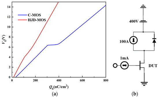
Figure 9.
(a) The gate charge of the C-MOS and the proposed structure. (b) The test circuit of the gate charge.
The switching characteristics of the two structures are shown in Figure 10. The test was applied with the typical testing circuit with the inductive load shown in Figure 10a. However, the reverse recovery current spike of the proposed structure is larger than the C-MOS because of the mismatch between the gate resistance and the decreased Cgd. The body diode of the C-MOS works as a bipolar device, while the HJD in the proposed structure works as a unipolar device. When the diode is turned off, the number of minority carriers in the proposed structure is much less than the C-MOS, leading to a smaller reverse recovery time (trr) and the reverse recovery charge (Qrr). Moreover, the reduced Cgd and Cgs brought by the shallow gate make further efforts to decrease the turn-on and turn-off time. As a result, the turn-on loss and turn-off loss decreased by 83.39% and 68.18% respectively, and the total switching loss is reduced by 77.78%, as can be seen in Figure 11.
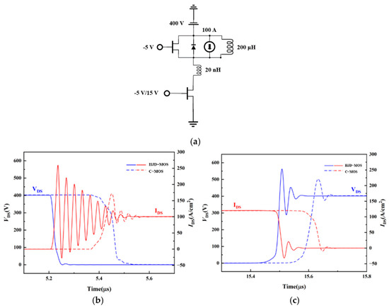
Figure 10.
(a) Double pulse test circuits. (b) Turn-on and (c) turn-off waveform of the C-MOS and the proposed structure.
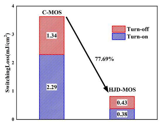
Figure 11.
The gate charge of the C-MOS and the proposed structure.
Table 2 Summarizes the electrical characteristics of the C-MOS and the proposed structure.
Table 2.
Device Characteristics.
4. Proposed Fabrication Process
Considering the feasibility of the proposed structure, the fabrication process is shown in Figure 12. The main process of the proposed structure is the same as the conventional structure but needs more steps to form the CSLs and the P+ poly-silicon. First, the N drift and the CSL1 region are formed by epitaxial growth on the N+ substrate. Then, the CSL2 and the deep P+ well are formed by ion implantation [25]. Then, on the top of the P+ well on the right, through double implantation [26], the P- base and the N+ source region are formed. After that, the HJD region and gate region are trenched at the same time. Then the gate is formed with thermal oxidation and poly-silicon deposition. HJD is then formed by depositing P+-doped poly-silicon. Lastly, the metal layer is connected to the source.
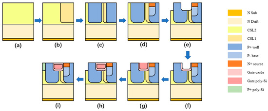
Figure 12.
The proposed fabrication process. (a) Epitaxial N- drift and CSL1 (b) Forming of CSL2 by ion implantation (c) Forming of P+ well by ion implantation (d) Forming of P- base and N+ source by double ion implantation (e) Annealing, trench gate region and HJD region (f) Thermal oxidation to form gate oxide (g) Depositing of gate poly-silicon (h) Depositing of gate oxide (i) Depositing of P+-doped poly-silicon of HJD region.
5. Conclusions
In this paper, a novel 650 V 4H-SiC trench MOSFET is proposed and studied by Sentaurus TCAD simulation which features a heterojunction diode and CSLs with different doping concentrations. The HJD helps to improve the third quadrant characteristics and recovery performance, while the CSLs provide a lower on-state resistance. Compared to C-MOS, the Ron, sp is decreased by 47.82%, the Qgd decreased by 82.78, and the switching loss is reduced by 77.78%, indicating a superior candidate in high-frequency situations.
Author Contributions
Conceptualization and Writing-Original draft, R.W.; Software, J.G.; Software and Data curation, C.L.; Software, H.W.; Software, Z.H.; Supervision and Writing-Reviewing and Editing, S.H. All authors have read and agreed to the published version of the manuscript.
Funding
This work is in part by the National Natural Science Foundation of China under Grant 62174017, in part by the Natural Science Foundation Project of CQ CSTC under Grant cstc2020jcyjmsxmX0243, and in part by the National Laboratory of Science and Technology on Analog Integrated Circuit under Grant 2021-JCJQ-LB-049-7.
Conflicts of Interest
The authors declare no conflict of interest.
References
- Casady, J.B.; Johnson, R.W.J.S.-S.E. Status of silicon carbide (SiC) as a wide-bandgap semiconductor for high-temperature applications: A review. Solid-State Electron. 1996, 39, 1409–1422. [Google Scholar] [CrossRef]
- Meli, A.; Muoio, A.; Reitano, R.; Sangregorio, E.; Calcagno, L.; Trotta, A.; Parisi, M.; Meda, L.; La Via, F. Effect of the Oxidation Process on Carrier Lifetime and on SF Defects of 4H SiC Thick Epilayer for Detection Applications. Micromachines 2022, 13, 1042. [Google Scholar] [CrossRef] [PubMed]
- Lee, G.; Ha, J.; Kim, K.; Bae, H.; Kim, C.E.; Kim, J. Influence of Radiation-Induced Displacement Defect in 1.2 kV SiC Metal-Oxide-Semiconductor Field-Effect Transistors. Micromachines 2022, 13, 901. [Google Scholar] [CrossRef] [PubMed]
- Liu, S.; Cheng, X.; Zheng, L.; Sledziewski, T.; Yu, Y. Impact of the transition region between active area and edge termination on electrical performance of SiC MOSFET. Solid-State Electron. 2020, 171, 107873. [Google Scholar] [CrossRef]
- Yano, K.; Nakazato, K. A high-current-gain low-temperature pseudo-heterojunction bipolar transistor utilizing sidewall base-contact structure (SICOS). IEEE Trans. Electron Devices 1991, 38, 555–565. [Google Scholar] [CrossRef]
- Grekov, A.; Maximenko, S.; Sudarshan, T.S. Effect of Basal Plane Dislocations on Characteristics of Diffused 4H-SiC p-i-n Diodes. IEEE Trans. Electron Devices 2005, 52, 2546–2551. [Google Scholar] [CrossRef]
- Kono, H.; Asaba, S.; Ohashi, T.; Ogata, T.; Furukawa, M.; Sano, K.; Yamaguchi, M.; Suzuki, H. Improving the specific on-resistance and short-circuit ruggedness tradeoff of 1.2-kV-class SBD-embedded SiC MOSFETs through cell pitch reduction and internal resistance optimization. In Proceedings of the 2021 33rd International Symposium on Power Semiconductor Devices and ICs (ISPSD), Nagoya, Japan, 30 May–3 June 2021; pp. 227–230. [Google Scholar]
- Ohashi, T.; Kono, H.; Kanie, S.; Ogata, T.; Sano, K.; Suzuki, H.; Asaba, S.; Fukatsu, S.; Iijima, R. Improved Clamping Capability of Parasitic Body Diode Utilizing New Equivalent Circuit Model of SBD-embedded SiC MOSFET. In Proceedings of the 2021 33rd International Symposium on Power Semiconductor Devices and ICs (ISPSD), Nagoya, Japan, 30 May–3 June 2021; pp. 79–82. [Google Scholar]
- Song, G.; Wang, Y.; Chen, X.; Li, C. Investigation on electrical characteristic of 3.3kV SiC MOSFET with integrated SBD. In Proceedings of the PCIM Asia 2021, International Exhibition and Conference for Power Electronics, Intelligent Motion, Renewable Energy and Energy Management, Shenzhen, China, 9–11 September 2021; pp. 1–4. [Google Scholar]
- Wu, Z.; Xia, C.; Yi, B.; Cheng, J.; Huang, H.; Kong, M.; Yang, H.; Shi, W. A split-gate SiC trench MOSFET with embedded unipolar diode for improved performances. In Proceedings of the 2021 IEEE 14th International Conference on ASIC (ASICON), Kunming, China, 26–29 October 2021; pp. 1–4. [Google Scholar]
- Huang, M.M.; Li, R.; Yang, Z.M.; Ma, Y.; Li, Y.; Zhang, X.; Gong, M. A Multiepi Superjunction MOSFET With a Lightly Doped MOS-Channel Diode for Improving Reverse Recovery. IEEE Trans. Electron Devices 2021, 68, 2401–2407. [Google Scholar] [CrossRef]
- Li, X.Y.; Jia, Y.P.; Zhou, X.T.; Zhao, Y.F.; Wu, Y.; Hu, D.Q.; Fang, X.Y.; Deng, Z.H. A Novel Split-Gate-Trench MOSFET Integrated With Normal Gate and Built-In Channel Diode. IEEE J. Electron Devices Soc. 2021, 9, 839–845. [Google Scholar] [CrossRef]
- Tanaka, H.; Hayashi, T.; Shimoida, Y.; Yamagami, S.; Tanimoto, S.; Hoshi, M. Ultra-low Von and High Voltage 4H-SiC Heterojunction Diode. In Proceedings of the ISPSD ’05, The 17th International Symposium on Power Semiconductor Devices and ICs, Santa Barbara, CA, USA, 23–26 May 2005; pp. 287–290. [Google Scholar]
- Na, J.; Kim, K. 3.3 kV 4H-SiC MOSFET with embeded hetero junction body diode for low switching loss. In Proceedings of the 2022 International Conference on Electronics, Information, and Communication (ICEIC), Jeju, Korea, 6–9 February 2022; pp. 1–4. [Google Scholar]
- Kim, J.; Kim, K. A novel 4H-SiC super junction UMOSFET with heterojunction diode for enhanced reverse recovery characteristics. In Proceedings of the 2020 International Conference on Electronics, Information, and Communication (ICEIC), Barcelona, Spain, 19–22 January 2020; pp. 1–4. [Google Scholar]
- Kim, J.; Kim, K. Single-Event Burnout Hardening 4H-SiC UMOSFET Structure. IEEE Trans. Device Mater. Reliab. 2022, 22, 164–168. [Google Scholar] [CrossRef]
- An, J.; Hu, S. Heterojunction Diode Shielded SiC Split-Gate Trench MOSFET With Optimized Reverse Recovery Characteristic and Low Switching Loss. IEEE Access 2019, 7, 28592–28596. [Google Scholar] [CrossRef]
- Yu, H.Y.; Liang, S.W.; Liu, H.Z.; Wang, J.; Shen, Z.J. Numerical Study of SiC MOSFET With Integrated n-/n-Type Poly-Si/SiC Heterojunction Freewheeling Diode. IEEE Trans. Electron Devices 2021, 68, 4571–4576. [Google Scholar] [CrossRef]
- Yang, T.T.; Wang, Y.; Yue, R.F. SiC Trench MOSFET With Reduced Switching Loss and Increased Short-Circuit Capability. IEEE Trans. Electron Devices 2020, 67, 3685–3690. [Google Scholar] [CrossRef]
- Okuto, Y.; Crowell, C.R. Threshold energy effect on avalanche breakdown voltage in semiconductor junctions. Solid State Electron. 1975, 18, 161–168. [Google Scholar] [CrossRef]
- Lombardi, C.; Manzini, S.; Saporito, A.; Vanzi, M. Physically based mobility model for numerical simulation of nonplanar devices. IEEE Trans. Comput.-Aided Des. Integr. Circuits Syst. 1988, 7, 1164–1171. [Google Scholar] [CrossRef]
- Lu, C.-Y.; Cooper, J.A.; Tsuji, T.; Chung, G.; Williams, J.R.; McDonald, K.; Feldman, L.C. Effect of Process Variations and Ambient Temperature on Electron Mobility at the SiO[sub 2]/4H-SiC Interface. IEEE Trans. Electron Devices 2003, 50, 1582–1588. [Google Scholar]
- Uchida, K.; Hiyoshi, T.; Nishiguchi, T.; Yamamoto, H.; Matsukawa, S.; Furumai, M.; Mikamura, Y. The Influence of Surface Pit Shape on 4H-SiC MOSFETs Reliability under High Temperature Bias Tests. Mater. Sci. Forum 2016, 858, 840–843. [Google Scholar] [CrossRef]
- Vudumula, P.; Kotamraju, S. Design and Optimization of 1.2-kV SiC Planar Inversion MOSFET Using Split Dummy Gate Concept for High-Frequency Applications. IEEE Trans. Electron Devices 2019, 66, 5266–5271. [Google Scholar] [CrossRef]
- Weijiang, Z.; Tobikawa, K.; Nagayama, T.; Sakai, S. A study on Silicon Carbide (SiC) wafer using ion implantation. In Proceedings of the 2014 20th International Conference on Ion Implantation Technology (IIT), Portland, OR, USA, 26 June–4 July 2014; pp. 1–4. [Google Scholar]
- Shen, H.-J.; Tang, Y.-C.; Peng, Z.-Y.; Deng, X.-C.; Bai, Y.; Wang, Y.-Y.; Li, C.-Z.; Liu, K.-A.; Liu, X.-Y. Fabrication and Characterization of 1700 V 4H-SiC Vertical Double-Implanted Metal-Oxide-Semiconductor Field-Effect Transistors. Chin. Phys. Lett. 2015, 32, 127101. [Google Scholar] [CrossRef]
Publisher’s Note: MDPI stays neutral with regard to jurisdictional claims in published maps and institutional affiliations. |
© 2022 by the authors. Licensee MDPI, Basel, Switzerland. This article is an open access article distributed under the terms and conditions of the Creative Commons Attribution (CC BY) license (https://creativecommons.org/licenses/by/4.0/).