Abstract
The continued growth of electric vehicle (EV) deployment has placed increasing emphasis on the development of charging infrastructure that is efficient, reliable, and compliant with safety requirements over a wide range of power levels. In EV charging systems, DC–DC converters work as a key interface for voltage adaptation, power regulation, and battery protection, making the choice of converter topology a crucial design consideration. This study provides a comparative and application-focused review of commonly employed isolated and non-isolated DC–DC converter topologies used in EV charging architectures. The comparison is carried out by examining voltage gain behavior, efficiency tendencies, switching and thermal stress, soft-switching capability, component utilization, control complexity, cost-related aspects, and practical deployment constraints. Fundamental operating principles and representative time-domain simulations are used to highlight relative performance trends of PWM-based and resonant isolated converters under typical charging conditions. Rather than introducing new converter structures or control methods, the objective of this work is to offer practical, design-oriented insights that support informed topology selection. Based on the comparative analysis, non-isolated converters are found to be well suited for low- to medium-power onboard charging applications, whereas isolated resonant converters are more appropriate for high-power and fast-charging systems when safety, scalability, efficiency trends, and system-level implementation factors are considered together.
1. Introduction
1.1. Background and Motivation
In recent years, the availability of energy has increasingly become a deciding factor for economic growth across the world. The continuous rise in power consumption across homes, industries and particularly the transportation sector has pushed traditional fossil-fuel-based energy systems to their limits. Along with this pressure, the environmental side effects of burning fossil fuels—air pollution, greenhouse gas emissions and the growing concern around climate imbalance—have encouraged policymakers and researchers to look seriously toward cleaner alternatives for mobility. Electric vehicles (EVs) have emerged as one of the strongest candidates in this transition toward decarbonization and long-term energy sustainability. As reported in [1,2,3], nearly 16.4 million EVs were already operating worldwide by the end of 2021, and this number is expected to approach 200 million by 2030 under the Stated Policies scenario. Such a steep rise does not only reflect user acceptance but also raises practical demands on the charging ecosystem. Today, EV users expect shorter charging time, improved battery safety and high energy efficiency—expectations that cannot be fulfilled without robust power conversion hardware. For this reason, DC–DC converters lie at the heart of every charging architecture. They are responsible for matching voltage levels, regulating power flow and protecting the battery during dynamic operating conditions. As charging power levels and battery capacities continue to increase, the performance of these converters becomes a crucial factor in achieving reliable, fast and safe charging experiences.
1.2. Related Work and Research Gap
The increasing use of two- and three-wheeled light electric vehicles (LEVs) has contributed significantly to the wider acceptance of electric mobility around the world. Their popularity is not surprising, since LEVs are inexpensive to operate, lightweight, and consume much less energy compared to conventional vehicles. They have become a practical choice for short-distance shared and public transport [4]. A major reason behind this growth is that most LEVs do not require elaborate charging infrastructure and can be recharged directly from a regular AC socket—something that has been observed with e-rickshaws and e-bikes in India [5], and in similar mobility initiatives across European countries [6].
As the range of EV categories continues to expand—from LEVs to high-performance passenger vehicles—the need for adaptable power conversion hardware becomes unavoidable. DC–DC converters play a central role here because charging involves not only voltage scaling, but also power flow regulation and battery safety [7]. They facilitate fast charging under fluctuating input conditions [8], support bidirectional energy exchange between the battery and the grid [9,10,11], and take care of low-voltage auxiliary electronics inside the vehicle [12]. Broadly, these converters are designed either as non-isolated or isolated structures, which groups the topologies according to their functional evolution. Choosing between these families has a major effect on cost, efficiency and safety in the charging system.
Even with many available designs, selecting an “ideal” converter remains complicated because performance requirements do not always complement one another. High-power fast charging, for example, demands converters that can withstand large currents and switching frequencies without compromising efficiency or generating excessive heat. Although wide-bandgap semiconductor devices have pushed efficiency and switching performance to new levels, their use introduces challenges in electromagnetic interference (EMI) suppression and overall system protection [13]. These competing considerations make the design space complex and highlight why identifying a suitable converter topology for EV charging is not straightforward. At the same time, converter topologies must cope with high-frequency noise, parasitic effects, and the need for compact magnetic components, all of which pose engineering difficulties. Resonant converters such as LLC achieve soft-switching and high power density but require accurate tuning to maintain efficiency under variable load conditions [14]. Furthermore, bidirectional converters suitable for V2G face additional complexity due to mode transition and stability concerns [15]. Although numerous converter structures have been developed for EV charging systems [16,17,18,19,20,21], existing research rarely presents a unified comparison between isolated and non-isolated topologies that simultaneously considers voltage gain, switching stress, soft-switching feasibility, EMI behavior, component count, bidirectional capability, and suitability across EV charging power levels.
In addition to the above studies, several high-gain and control-oriented DC–DC converter topologies have been reported by the present authors for renewable and DC microgrid applications, including ADRC-controlled high-gain boost and switched-capacitor-based converters [22,23], as well as SEPIC-derived non-isolated buck–boost structures and maximum-sensitivity-based ADRC control schemes for boost converters [24,25]. These works primarily focus on proposing and experimentally validating specific converter or control architectures. By contrast, the present manuscript aims to provide a broader comparative performance perspective across isolated and non-isolated converter families for EV charging applications, thereby complementing these earlier topology- and control-centric contributions.
To summarize, although a wide range of isolated and non-isolated DC–DC converter configurations has been developed for electric vehicle charging, most existing studies analyze these topologies individually rather than from a unified perspective. The literature rarely correlates voltage gain capability, switching and thermal stress, soft-switching behavior, efficiency trends, EMI performance, bidirectional feasibility, and suitability across different EV charging power levels within a single comparative framework. Because most previous studies focus on individual converter designs without relating them directly to real EV charging conditions, researchers and engineers are still left with uncertainty when trying to select the most suitable topology for a specific charging application. In practice, the decision is rarely obvious, since charging power levels, safety needs and cost targets vary widely across EV categories. This situation clearly signals the need for a single, application-focused comparison that evaluates isolated and non-isolated DC–DC converters side by side, specifically in the context of EV charging requirements.
1.3. Major Contributions
To bridge the gaps highlighted earlier, this work puts forward a focused comparison of various DC–DC converter topologies that are currently used in EV charging systems. The contributions of the study can be outlined as follows:
- A structured examination of both non-isolated converters (buck, boost, buck–boost and Ćuk) and isolated converters (flyback, resonant SLR and resonant LLC) that appear frequently in EV charging applications.
- Interpretation of their operating mechanisms using circuit-level and system-level analytical modeling rather than relying only on theoretical descriptions.
- A side-by-side comparison of key performance indicators such as voltage gain, conversion efficiency, switching stress, soft-switching capability, EMI behavior, control difficulty and suitability across different EV charging power levels.
- Practical guidance on selecting a suitable converter topology depending on the EV segment, rated charging power and intended features such as V2G support or compact on-board charging.
1.4. Paper Orientation
The rest of the manuscript is organized to provide a smooth technical progression. Section 2 summarizes the main non-isolated and isolated DC–DC converter topologies and explains their operating principles. Section 3 presents the comparative analysis based on analytical performance parameters. Section 4 discusses simulation findings and interprets the trends obtained. Finally, Section 5 closes the paper by highlighting important observations and possible research directions.
2. Broad Classification of DC-DC Converters
DC–DC converters used in EV charging systems can be broadly classified into non-isolated and isolated topologies based on whether galvanic isolation exists between the input and output stages. Non-isolated converters provide direct electrical coupling and are typically favored for low- to medium-power applications where cost, compactness, and simplicity are prioritized. In contrast, isolated converters employ transformers or high-frequency isolation mechanisms to provide electrical separation, which is essential in high-voltage, high-power, and safety-critical EV charging environments. This classification forms the basis for the comparative analysis presented in the following sections.
DC–DC converters have gradually become one of the most essential building blocks in modern power-electronic systems, and many researchers over the years have attempted to improve their efficiency, dynamic behavior and control strategies. In this context, the literature reports a wide range of converter structures—for example, buck, boost, buck–boost, multilevel, resonant and ZVS-based designs—each introduced to solve a particular limitation of earlier approaches. For the sake of clarity, these converters are usually grouped into two broad categories: isolated and non-isolated. Within each category, several circuit variations exist, and they differ not only in their physical structure but also in the way they operate, regulate power and interface with different applications.
2.1. Non-Isolated DC-DC Converters
As illustrated in Figure 1, several variants of non-isolated converter structures exist, each designed with a particular purpose in mind. Over the past few years, researchers have been actively experimenting with newer circuit configurations and improved control approaches in order to meet the very different power requirements seen in applications such as portable devices, renewable-energy interfaces and electric vehicle systems.
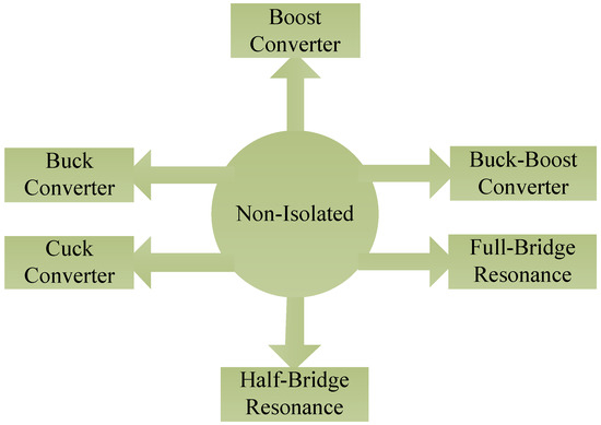
Figure 1.
Type of non-isolated converters.
2.1.1. Buck Converter
A buck converter is a circuit that has the capacity to step down the output voltage relative to the input voltage [26,27,28]. The circuit diagram for this converter is shown in Figure 2. The circuit of this converter consists of a single switch that is connected in series to the input voltage source. The switch is operated with the proper PWM signal that is desired for a particular output voltage level. These kinds of converters can be used to integrate lower battery voltage with higher grid voltages. These can also be used for rural PV-based pumping systems and solar battery chargers. The relation between output and input voltage is given by
The circuit operates in two modes depending on the ON and OFF positions of the switch.
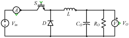
Figure 2.
Circuit diagram of a buck converter.
The state matrix during ON mode is given by
where is the current through the inductor, is the voltage across the capacitor, represents output voltage and is the source voltage. Similarly, the state matrix during OFF mode can be represented as
The final state matrix is deduced by the state space averaging technique. Therefore, the overall state matrix is represented as
Here, d denotes the duty ratio of the switching signal, while the symbol D is used exclusively to represent the diode in the circuit diagrams. In Equations (1)–(4), d is defined as the ratio of the switch ON duration to the total switching period. It indicates how long the input source is connected to the converter during each switching cycle. By adjusting d, the average voltage applied to the reactive elements is modified, which in turn regulates the output voltage and steady-state behavior of PWM-based DC–DC converters. The simulation results depicting the load voltage, source current, source voltage, and switching signal are shown in Figure 3.
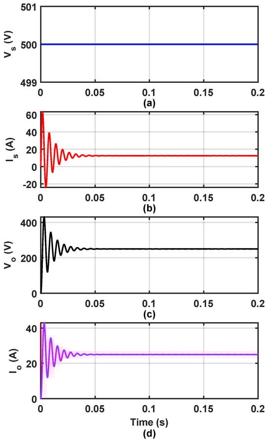
Figure 3.
Time-domain simulation responses of the buck DC–DC converter showing (a) source voltage, (b) source current, (c) load voltage, and (d) load current, illustrating steady-state step-down voltage operation under PWM control.
2.1.2. Boost Converter
A boost converter is a particular kind of DC–DC converter that is used to boost the voltage provided to it [29,30]. The duty cycle of the switch determines the output voltage. At a duty cycle of 0.5, an output that is equal to double the input voltage is obtained. Figure 4 depicts the boost converter’s circuit diagram. Wherever a higher output voltage is required than the input voltage, this converter is widely used. To gain the most power output from the panel, it can also be integrated with PV panels using MPPT techniques. The resulting response from the simulation is displayed in Figure 5.
Figure 4.
Circuit diagram of a boost converter.
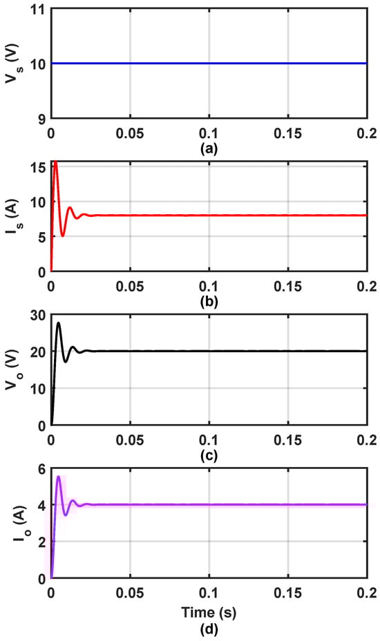
Figure 5.
Simulated transient and steady-state waveforms of the boost DC–DC converter comprising (a) input source voltage, (b) source current, (c) output voltage, and (d) load current, demonstrating step-up voltage conversion.
It again has two operating modes that are dependent on the switch’s ON and OFF states. The equations for the ON state are as follows:
Similarly, the equation describing the OFF mode is given by
The averaged equation is given by
2.1.3. Buck–Boost Converter
A buck–boost converter can increase or decrease the output voltage in relation to the input voltage depending on the duty ratio [30]. The circuit operates in buck mode when the duty ratio is less than 0.5 and in boost mode when it is larger than 0.5. The reversed output voltage of this converter is a disadvantage. Figure 6 depicts the circuit diagram for this converter. Additionally, Figure 7 displays the converter’s simulation results. Additionally equipped with a switch, this converter has two operational modes that are determined by the switch’s ON and OFF settings. The state equations for ON mode are given by
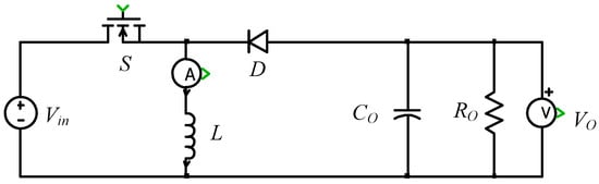
Figure 6.
Circuit diagram for a buck–boost converter.
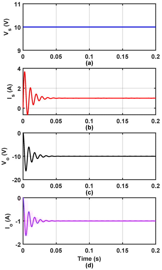
Figure 7.
Simulation responses of the buck–boost DC–DC converter showing (a) source voltage, (b) source current, (c) output voltage, and (d) load current, highlighting bidirectional voltage gain with inverted output polarity.
2.1.4. Ćuk Converter
A Ćuk converter is also a buck–boost converter that provides inverted output voltage. This converter has some benefits over a conventional converter, such as the continuous input and output current [31]. However, the voltage stress on the switches in this converter increases compared to a conventional converter. Unlike a conventional buck–boost converter where the energy is stored in the inductor, the energy in a Ćuk converter is stored in the capacitor. Bidirectional energy can be flown by the use of a diode and MOSFET. These converters are of two types, isolated and non-isolated type. The circuit diagram for a non-isolated type Ćuk converter is shown in Figure 8. The simulation results for a Ćuk converter are displayed in Figure 9.
Figure 8.
Circuit diagram for a Ćuk converter.
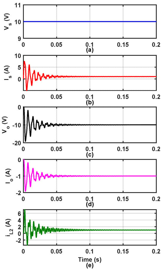
Figure 9.
Time-domain responses of the Ćuk converter depicting (a) source voltage, (b) source current, (c) output voltage, (d) load current, and (e) intermediate inductor current, emphasizing continuous input and output current characteristics.
The voltage gain equation of a Ćuk converter is given as
The equation corresponding to the ON state of the switch is given by
The equation corresponding to the OFF state of the switch is given by
After applying the state space averaging technique, the averaged state matrix is obtained as
2.1.5. Half-Bridge Series Loaded Resonant (SLR) Converter
The SLR converter is a kind of DC–DC converter that is used to provide better power quality than a conventional converter [32]. It can be operated with zero voltage switching (ZVS) and zero current switching (ZCS) on turn-on and turn-off processes respectively. These converters have a wide range of applications such as in generation systems like PV systems, fuel cells, wind generation systems, and aero generators, etc. The switching losses in these types of converters are considerably reduced due to the ZVS and ZCS of the switches.
Figure 10 depicts the circuit layout for a half-bridge SLR. A half-bridge inverter, an LC tank circuit, and a rectifier that changes AC back to DC at the load end compose the circuit. The circuit’s characteristic impedance and series resonance are provided by LC components.
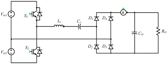
Figure 10.
Circuit diagram of a half-bridge SLR converter.
As a result, the frequency at which a circuit is run determines how it operates. If the operational frequency (fs) is less than one-half of the resonant frequency (), the circuit runs in discontinuous conduction mode (DCM). A 50 % duty cycle is used to alternately operate the two switches. The current in discontinuous mode decreases to zero during the freewheeling period. Additionally, the output voltage that is obtained after the tank circuit is not perfectly sinusoidal.
If the operating frequency is more than 50 % of the resonant frequency, the circuit operates in continuous conduction mode (CCM). This situation can have two different outcomes, such as when the switching frequency is more than the resonant frequency () or when it is less than the resonant frequency but greater than half of it (). After the tank circuit, both situations provide output voltage and current that are strictly sinusoidal. However, in the first scenario, the voltage comes first, whereas in the second, the current comes first. Figure 11 displays the simulation result showing the output voltage, source voltage, resonance current, and load current. You can specify the resonant frequency as
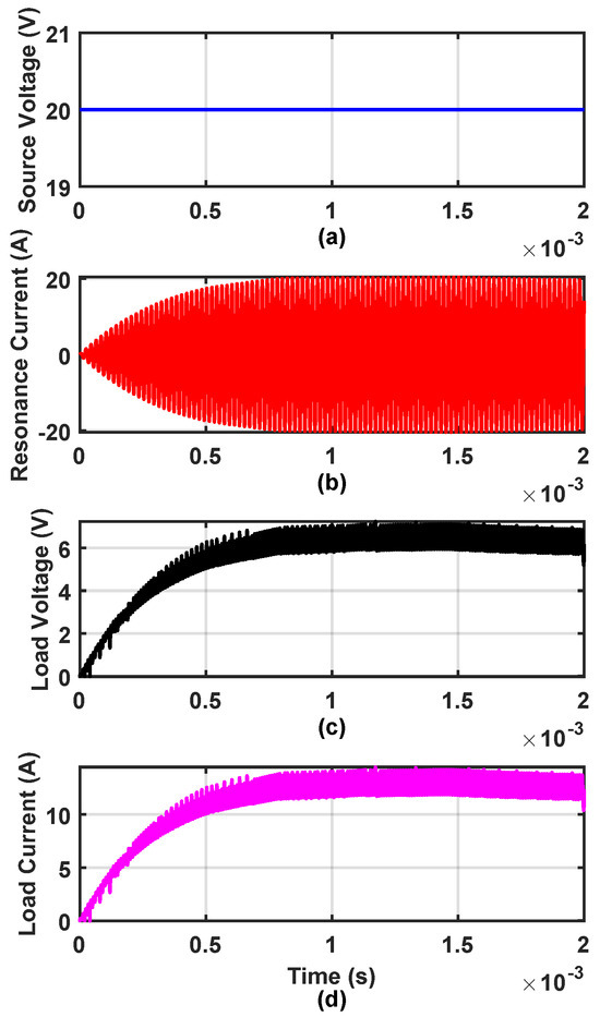
Figure 11.
Simulation results of the half-bridge series-loaded resonant (SLR) converter showing (a) source voltage, (b) resonant tank current, (c) load voltage, and (d) load current, illustrating soft-switching behavior and resonant energy transfer.
2.1.6. Full-Bridge Series Loaded Resonant (SLR) Converter
A full-bridge SLR circuit is shown in Figure 12 [33]. The circuit is named after the full-bridge inverter present in the circuit. Other circuit components are similar to that of a half-bridge SLR. The tank circuit operates in a similar way as the half-bridge SLR circuit. However, a single battery voltage is required at the input side, which enhances the power rating of the circuit. In this case, MOSFETs are turned ON simultaneously to complete the circuit. The inverter produces a square wave at its output and this square wave is converted into a sinusoidal wave after passing it through the tank circuit. The simulation result depicting the output voltage, source voltage, resonance current, and load current are displayed in Figure 13. The tank circuit has a resonant frequency which is given as
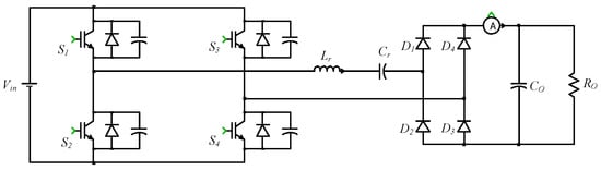
Figure 12.
Circuit diagram of a full-bridge SLR converter.
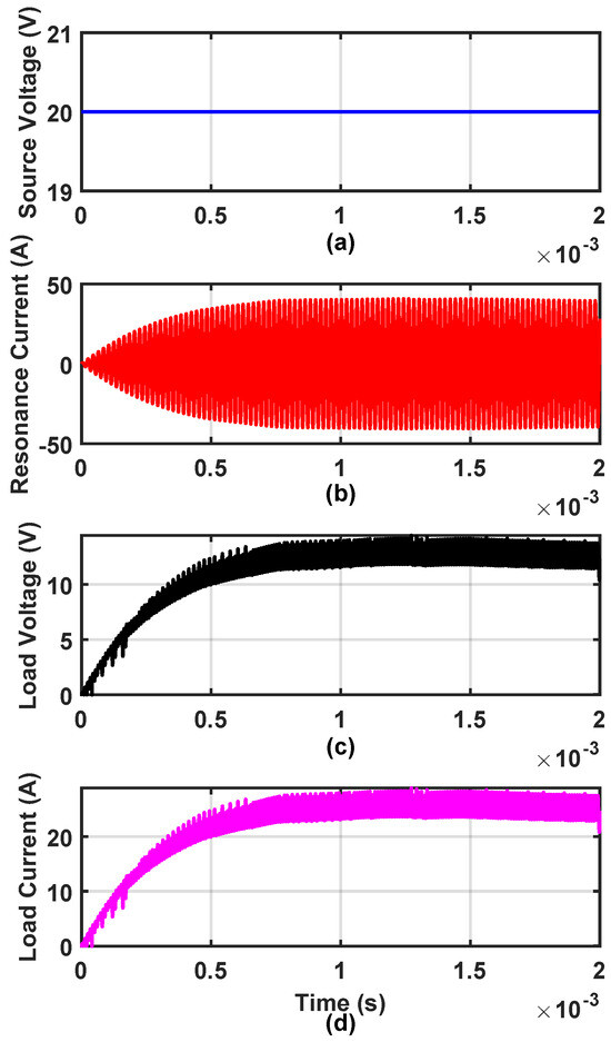
Figure 13.
Time-domain simulation responses of the full-bridge SLR converter comprising (a) source voltage, (b) resonant current, (c) output voltage, and (d) load current, demonstrating enhanced power capability compared to the half-bridge configuration.
Similar to a half-bridge SLR, this circuit also has three modes of conduction depending on the level of switching frequency.
Discontinuous conduction mode.
Continuous conduction mod.
Continuous conduction mode.
The sinusoidal voltage produced by the tank circuit is fed to the rectifier which produces a pulsating output. Hence, to get a pure DC output, a filter capacitor () is introduced at the load side. the selection of the circuit components is done according to the resonant and switching frequency. The output voltage keeps on increasing as the frequency of operation is increased.
2.2. Isolated Type DC–DC Converter
Isolated DC–DC converters represent a specialized category of converters designed to create electrical separation between the input and output stages. This isolation is accomplished by integrating transformers or other isolation mechanisms into the converter’s structure. Isolated DC–DC converters are commonly employed in applications where electrical safety, noise immunity, and galvanic isolation are essential design requirements. Their primary advantages include improved user and equipment safety, reduced susceptibility to electromagnetic interference, and the ability to decouple input and output voltage levels. As a result, these converters are widely adopted in sectors such as medical instrumentation, aerospace electronics, telecommunications infrastructure, and industrial automation systems, where isolation is mandated by standards or operational constraints. Ongoing research and development efforts continue to focus on improving the efficiency, reliability, and power handling capability of isolated DC–DC converters to address the increasing performance demands of modern power electronic systems.
2.2.1. Flyback Converter
A flyback converter is a kind of buck–boost converter that can be used in both AC to DC and DC to DC power conversion with isolation between the input and output circuits [34,35]. The inductor is split into two parts with the help of a transformer. This isolates the input and output side, allowing the extra voltage gain that may be induced by controlling the transformer’s turn ratio. The circuit diagram of this converter is shown in Figure 14. Its simulation results are shown in Figure 15.
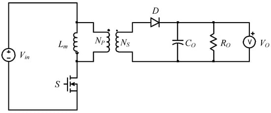
Figure 14.
Circuit diagram of a flyback converter.
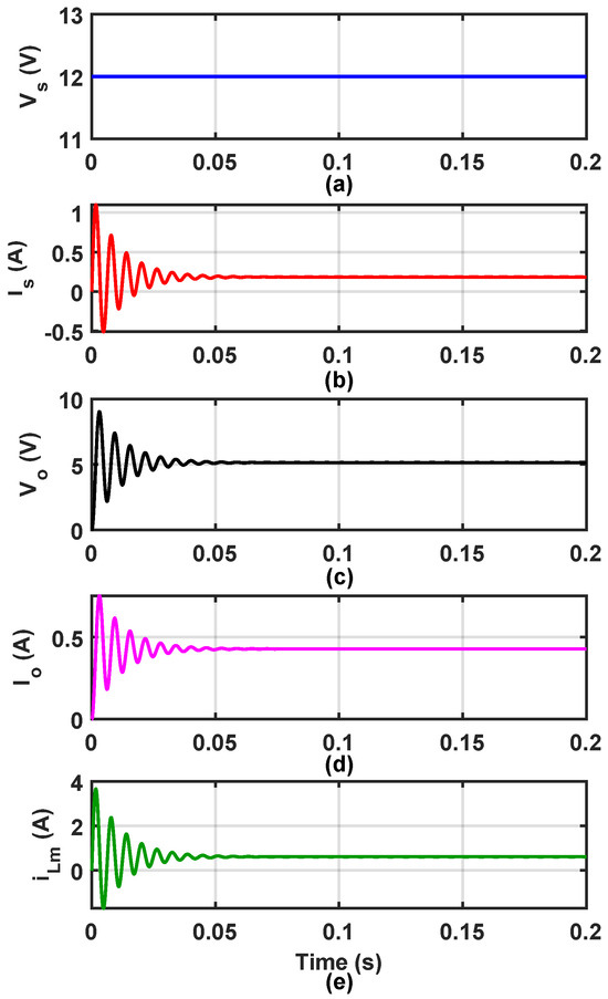
Figure 15.
Simulated waveforms of the flyback converter showing (a) input voltage, (b) source current, (c) output voltage, (d) load current, and (e) magnetizing inductor current, illustrating isolated step-up/step-down operation.
The working of this converter is similar to a normal buck–boost converter. It is different only by the split action of the inductor that makes it isolated. It can be used to get multiple outputs. It can be used for low-power switched-mode power supplies for mobile and laptop chargers, multiple output supplies, gate driver circuits that may be isolated, high voltage gain applications, etc. It has some limitations as the control of the converter both in the voltage-controlled scheme and the current-controlled scheme are complex due to the presence of right half-plane zeroes. The state equations are similar to that of a conventional buck–boost converter.
For ON state, the state equations are evaluated as
For the OFF state of the switch, the state equations can be written as under
After the state space averaging technique, the final state space can be written as
2.2.2. Half-Bridge Resonant LLC Converter
LLC converters are known for their high power density and high efficiency. These converters work either on series resonance or parallel resonance networks [36,37]. Among other resonant topologies, these converters find many advantages such as zero voltage switching for the MOSFETs on the primary side and zero current switching for the MOSFETs on the secondary or load side. The secondary side consists of a half-bridge rectifier; hence, it finds the name half-bridge LLC converter. The converter as shown in Figure 16 consists of two MOSFETs which are switched ON and OFF alternately with a duty cycle of 50 % with some dead bands so that the two switches cannot be in an ON state simultaneously.
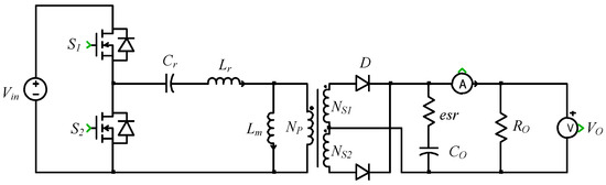
Figure 16.
Circuit diagram of a half-bridge resonant LLC converter.
The resonant circuit is built up of two inductors and a capacitor. These include a series inductance , a series capacitor , and a small magnetizing inductance of the transformer. The turns ratio of the transformer is denoted as n. The energy is transferred from the primary side to the secondary side by the transformer action; hence, the voltage gain can be manipulated depending on the turns ratio. The transformer also provides electrical isolation to the circuit. A bipolar square wave is fed to the primary side of the transformer. The secondary side of the converter consists of a full wave rectifier that converts the AC into DC for supplying the load with the help of a filter capacitor .
The circuit consists of a series resonance with a resonant frequency given as
This circuit has a property that its frequency at peak resonance is always equal to the resonant frequency. After adding the magnetizing inductance , the peak resonant frequency becomes a function of load that varies between . Hence, in this case, the resonant frequency can be described as
Hence, at no load, . As the load value increases, the moves towards the . Again, in a short circuit condition, occurs.
The responses obtained from the simulation are shown in Figure 17. The operation of this converter is dependent on the relation between the switching frequency of the switches and the resonant frequency of the series resonant circuit.
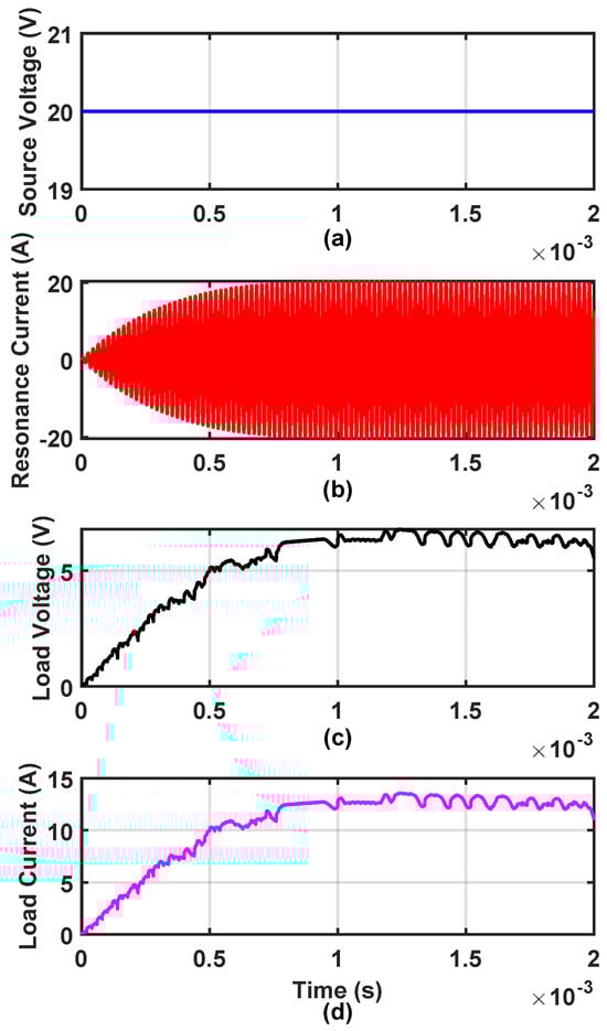
Figure 17.
Simulation responses of the half-bridge resonant LLC converter depicting (a) source voltage, (b) resonant tank current, (c) load voltage, and (d) load current, highlighting soft-switching operation and reduced output ripple.
Therefore, the mode of operation is according to the frequency equal to the resonant frequency, greater than the resonant frequency, and less than the resonant frequency. The best frequency for the design purpose is the frequency close to the series resonant frequency.
2.2.3. Full-Bridge Resonant LLC Converter
This converter consists of a full-bridge converter (with four MOSFETs ()) for producing square wave, a series resonance circuit (consisting of , and ), a transformer for isolation and providing desired voltage gain depending on the turns ratio and a rectifier on the secondary side [38]. The circuit diagram of a full-bridge LLC converter is shown in Figure 18. The responses obtained from the simulation are shown in Figure 19.
Figure 18.
Circuit diagram for a full-bridge resonant LLC converter.
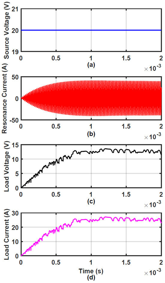
Figure 19.
Time-domain simulation results of the full-bridge resonant LLC converter showing (a) source voltage, (b) resonant current, (c) output voltage, and (d) load current, demonstrating high-power operation with improved voltage regulation.
The switching of the MOSFETs is done in pairs of and and and . These pairs are turned ON and OFF alternately with a duty cycle of 50%. For the switching transitions, a small dead time is given so that the source does not get short-circuited. The dead time also gives time for zero voltage switching of the MOSFETs. There are two resonant frequencies depending upon the resonant components:
and
The power is distributed in two switching cycles such that the current resonates in the tank circuit, once in the positive direction and then in the negative direction. The energy is transferred from the primary to the secondary side with the help of the transformer action. The current in the primary of the transformer is the difference between the magnetizing current and the resonating current. Similar to the half-bridge LLC, the operation is dependent on the load that changes the frequency of operation. With the increase in the load, the switching frequency shifts toward the resonating frequency. The operating principle on the load side is similar to that of the half-bridge LLC. The AC is converted into DC by the use of a bridge rectifier, and with the help of a filter capacitor of large value, a constant DC is received at the output.
3. Comparative Analysis of Isolated and Non-Isolated DC–DC Converters
3.1. Evaluation Framework and Comparison Criteria
The comparative analysis in this section is intended to identify DC–DC converter topologies that are suitable for electric vehicle charging applications operating under different practical conditions. Instead of focusing on absolute numerical performance values, the assessment concentrates on relative performance tendencies and system-level trade-offs that are more meaningful from an EV charger design perspective. For consistency across converter families, the analysis is conducted using representative operating conditions, comparable input voltage ranges, and similar loading scenarios.
The comparative evaluation is carried out using representative operating conditions commonly encountered in EV charging systems. Low-, medium-, and high-power ranges associated with onboard charging, fast charging, and ultra-fast charging infrastructures are considered. The corresponding input and output voltage levels are aligned with widely used EV battery and DC-link standards. Switching frequency, semiconductor technology, and load characteristics are selected in a representative manner for each converter family, since enforcing identical numerical benchmark conditions across fundamentally different topologies may lead to unrealistic or misleading comparisons.
To improve the clarity and reproducibility of the comparative simulations, the representative operating conditions and key simulation parameters used across the different converter topologies are summarized in Table 1.

Table 1.
Representative simulation parameters used for comparative analysis.
The listed parameters are intentionally selected to support normalized, trend-oriented comparison of converter behavior; different input voltage levels are used for individual topologies to illustrate scalable operating characteristics rather than to represent a single fixed EV battery voltage.
To organize the comparison, the evaluation criteria are grouped into two complementary categories. Table 2 outlines performance-oriented aspects such as voltage gain capability, efficiency trends, switching behavior, and thermal stress, which directly influence electrical performance and operational reliability. Table 3, on the other hand, emphasizes system-level and implementation-related factors, including applicable power range, isolation requirements, magnetic component complexity, control strategy, scalability, and typical application domains. Together, these tables establish a structured basis for comparative assessment and practical topology selection.
Table 2.
Performance-oriented comparison of DC–DC converter topologies for EV charging applications.
Table 3.
System-level and implementation-oriented comparison of DC–DC converter topologies for EV charging applications.
The qualitative descriptors used in Table 2 and Table 3 (such as high, medium, and low) are intended to indicate relative performance trends among converter families rather than absolute quantitative thresholds. These labels summarize commonly reported behavior across representative operating ranges and are consistent with their typical use during early-stage converter topology selection for EV charging applications. The classifications are, therefore, comparative in nature and should be interpreted in relation to the assumed operating context rather than as fixed numerical limits.
The comparison framework adopted in this study relies on commonly accepted evaluation metrics relevant to EV charging systems. These metrics include efficiency behavior under representative operating conditions, switching and ripple characteristics inferred from time-domain responses, thermal stress and component rating considerations, reliability-related aspects such as stress distribution and fault sensitivity, and scalability, power density tendencies, and relative cost implications. All metrics are examined in a qualitative and comparative manner using consistent assumptions, enabling transparent and balanced comparison across different DC–DC converter topologies.
3.2. Application-Oriented Comparison of Converter Families
3.2.1. Non-Isolated DC–DC Converters
Non-isolated DC–DC converter topologies, including buck, boost, buck–boost, and Ćuk converters, are commonly employed in EV charging systems where galvanic isolation is not a strict requirement [7]. These converters are generally characterized by relatively simple circuit structures, duty-ratio-based PWM control, and a modest number of components. As reflected in Table 2, they can achieve high efficiency at low to moderate power levels, with voltage conversion primarily controlled through adjustment of the duty ratio.
From a system-level viewpoint, the characteristics summarized in Table 3 indicate that non-isolated converters involve low magnetic complexity, straightforward control implementation, and comparatively limited EMI mitigation effort. These attributes make them suitable for applications such as low-power onboard chargers, auxiliary DC buses, and intermediate voltage regulation stages within EV power architectures. However, when operated at higher power levels or extreme duty ratios, conduction and switching losses increase significantly, resulting in higher thermal stress and reduced efficiency. As a result, the scalability of non-isolated converters is limited, and their use in high-power EV charging systems is generally restricted.
3.2.2. Isolated DC–DC Converters
Isolated DC–DC converters achieve electrical separation between the input and output stages by means of high-frequency transformers, thereby improving operational safety and enabling wider voltage adaptation. Because of these features, they are widely adopted in high-voltage battery systems, off-board chargers, and fast-charging installations. As indicated in Table 2, isolated converter topologies generally offer greater flexibility in voltage gain and improved distribution of electrical stress across power devices.
Within this category, flyback converters provide a relatively simple and cost-effective solution for low-power applications, owing to their reduced switch count and comparatively straightforward control implementation. Their performance, however, deteriorates at higher power levels due to increased losses and thermal stress. Resonant isolated converters, including series-loaded resonant (SLR) and LLC topologies, are designed to mitigate these limitations in medium- to high-power EV charging applications by enabling soft-switching operation and improved efficiency trends, subject to appropriate resonant tank design and control implementation [39]. By operating under soft-switching conditions, these converters significantly reduce switching losses and device stress, which enhances efficiency and scalability, as summarized in Table 2 and Table 3. These benefits are achieved at the expense of higher magnetic component complexity and increased control effort.
The importance of galvanic isolation in EV charging systems is closely linked to safety and regulatory compliance, and its necessity varies with the charging configuration. In on-board charging systems, isolation is primarily intended to protect vehicle occupants and sensitive low-voltage electronics from faults originating in the high-voltage battery system. In contrast, station-side DC chargers and fast-charging infrastructure operate under stricter isolation requirements due to elevated voltage levels, direct interaction with the power grid, and public accessibility, all of which demand compliance with insulation coordination and leakage current standards.
From a system safety and grid-integration perspective, galvanic isolation provides a controlled barrier that limits ground-fault currents and suppresses common-mode noise coupling between the grid and the vehicle [11]. These characteristics are particularly critical in medium- to high-power charging stations, where electromagnetic compatibility and fault tolerance are major design concerns. As a result, isolated DC–DC converter topologies are generally preferred for medium- and high-power EV charging applications, while non-isolated converters are typically restricted to low-power or auxiliary functions where safety and regulatory constraints are less demanding.
3.3. Comparative Discussion and Design Implications
The comparative results discussed in this section are intended to highlight representative operating behavior and relative performance trends of different DC–DC converter families used in EV charging systems. Detailed charging profiles such as full constant-current/constant-voltage (CC–CV) charging trajectories, wide battery voltage sweeps, and light-load operating conditions are not explicitly implemented, as these depend strongly on topology-specific control strategies, tuning methods, and protection mechanisms. Nevertheless, the observed trends provide meaningful insight into how different converter topologies respond to variations in operating conditions, particularly in terms of voltage adaptability, efficiency behavior, soft-switching range, and scalability, which are critical considerations in practical EV charging and bidirectional energy exchange scenarios [40].
3.3.1. Performance Trade-Offs
The relative advantages and limitations of isolated and non-isolated DC–DC converters stem from inherent design trade-offs rather than from any single performance indicator. From an efficiency standpoint, the non-isolated PWM-based converters typically perform well at low to moderate power levels, largely due to their reduced component count and the absence of any transformer-related losses. As the required voltage conversion ratio and operating power increase, however, conduction and switching losses rise noticeably, leading to higher thermal stress, a trend that is consistent with the comparative behavior summarized in Table 2.
Isolated converters, on the other hand, are commonly selected to meet safety and galvanic isolation requirements that are essential in the high-voltage EV charging environments. Resonant isolated topologies further mitigate efficiency and thermal constraints by operating under soft-switching conditions, which lowers switching losses and reduces stress on power devices at elevated power levels. In addition, considerations related to grid interfacing and electromagnetic compatibility increasingly favor isolated architectures, particularly in station-side fast-charging systems where regulatory limits on leakage current and electromagnetic emissions are more stringent [41]. These observations suggest that converter performance should be evaluated in relation to efficiency objectives, safety compliance, and grid-integration demands, rather than being interpreted as an absolute measure of the converter superiority.
3.3.2. Cost and Implementation Considerations
Cost plays a decisive role in the practical design of EV chargers and must be assessed in conjunction with electrical performance requirements. In this study, cost implications are examined on a relative basis by accounting for factors such as component count, magnetic component complexity, semiconductor device ratings, auxiliary circuit requirements, and the effort associated with control implementation. As summarized in Table 3, non-isolated converter topologies generally involve lower implementation cost because of their simpler structures and reduced component usage, which makes them attractive for cost-sensitive charging applications.
Isolated DC–DC converters, by contrast, inherently involve higher cost due to the inclusion of transformers and isolation-related circuitry. Within this group, flyback converters offer a comparatively economical isolated solution for low-power applications, whereas resonant topologies require more complex magnetic components and advanced control schemes. For medium- to high-power EV charging systems, however, the additional cost associated with resonant converters is often offset by improved efficiency trends, reduced thermal management burden, and better scalability, which can justify their adoption in demanding charging scenarios.
3.3.3. Topology Selection Guidelines for EV Charging Applications
By jointly considering the performance-oriented characteristics summarized in Table 2 and the system-level attributes presented in Table 3, clear topology selection guidelines can be established for EV charging applications. For low-power and cost-sensitive onboard chargers where galvanic isolation is not mandatory, non-isolated PWM-based converters provide a practical and efficient solution. When electrical isolation is required at low power levels, flyback converters offer an appropriate compromise between simplicity and performance.
For medium- to high-power EV charging systems, particularly in off-board and fast-charging applications, isolated resonant converters such as SLR and LLC topologies are more suitable due to their high efficiency, reduced switching losses, improved thermal performance, and superior scalability. Consequently, EV charger designers should prioritize topology selection based on charging power level, voltage conversion requirements, isolation needs, efficiency–cost trade-offs, and control complexity rather than seeking a single universally optimal converter architecture.
Functional aspects such as bidirectional power flow and potential vehicle-to-grid (V2G) capability are treated at a comparative level in the subsequent analysis and are summarized later in the manuscript alongside other implementation-oriented considerations.
To further clarify the relationship between converter selection and practical EV charging scenarios, a structured use-case mapping is summarized in Table 4.
Table 4.
Mapping of DC–DC converter topologies to EV charging scenarios.
3.4. Summary of Comparative Findings
The comparative evaluation presented in Table 2 and Table 3 highlights that isolated and non-isolated DC–DC converter topologies fulfill distinct yet complementary roles within EV charging systems. Non-isolated converters are particularly effective at low power levels, where simplicity, compact implementation, and cost efficiency are primary considerations. As charging power increases and stricter requirements related to efficiency, safety, and reliability come into play, isolated resonant converters offer clear advantages. By consolidating performance- and system-level insights, this comparison provides a practical basis for informed topology selection in contemporary EV charger design.
4. Results and Discussion
In order to perform a comparative evaluation of isolated and non-isolated DC–DC converter topologies for electric vehicle (EV) charging systems, analytical models were implemented in MATLAB. The voltage gain and efficiency expressions were formulated for five PWM-based converters (buck, boost, buck–boost, Ćuk, and flyback) and four isolated resonant converters (half-bridge SLR, full-bridge SLR, half-bridge LLC, and full-bridge LLC). Typical semiconductor parameters were assumed for illustration purposes (, , per transition), representing medium-voltage MOSFETs and fast-recovery diodes commonly employed in on-board and off-board EV chargers. The objective of this simulation study was to highlight relative performance trends among topologies rather than to reproduce a specific hardware design.
Accordingly, the efficiency values discussed in this section and summarized in the comparative tables represent typical literature-reported performance under optimized conditions and are intended for relative comparison rather than as universally guaranteed efficiency levels across all operating envelopes.
4.1. Performance of PWM-Based Converters
Figure 20 presents the three-dimensional relationship between duty ratio (D), voltage gain (), and conversion efficiency () for the considered PWM-based converters. Three characteristic operating regions are observed:
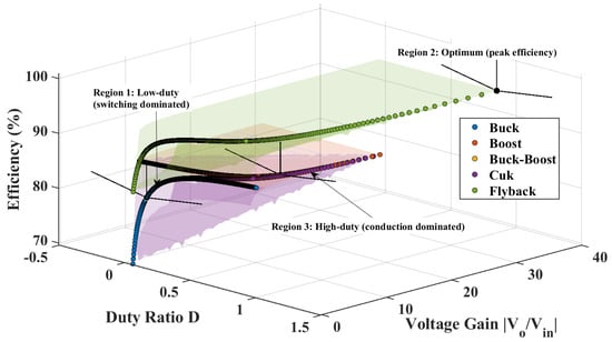
Figure 20.
Three-dimensional plot showing the effect of duty ratio on voltage gain and efficiency of PWM-based DC–DC converters.
- Region 1 (Low-duty/Switching-dominated): At small duty ratios, the switching frequency is relatively high and switching losses dominate. The converters operate with low current stress but exhibit moderate efficiency levels.
- Region 2 (Optimum region): In the mid-duty range (), the switching and conduction losses counterbalance each other, and the converter typically reaches its highest efficiency. For most non-isolated converters, this range is usually considered the most favorable operating zone.
- Region 3 (High-duty/Conduction-dominated): As the duty ratio continues to increase, the current passing through the components rises as well, and the extra resistive and diode losses gradually pull down the efficiency.
Comparing the converters further, boost and flyback units are capable of achieving higher voltage gains, but they often do so at the cost of efficiency because of increased conduction loss. The buck converter behaves almost the opposite—it delivers only step-down gain but is generally more efficient, which is why it is preferred for low-voltage applications. Buck–boost and Ćuk converters fall somewhere between the two, offering step-up and step-down capability with moderate efficiency, making them adaptable to a wider range of operating conditions.
4.2. Performance of Resonant-Isolated Converters
The analytical plots of gain and efficiency for isolated resonant converters are presented in Figure 21, where both parameters are expressed with respect to the normalized switching frequency . From these surfaces, three operating regions can clearly be observed:
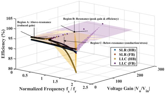
Figure 21.
3D plot showing how voltage gain and efficiency are affected with normalized switching frequency in resonant isolated converters.
- Region A (Above resonance): When is greater than unity, the converter behaves mainly in the inductive region. Although ZVS is still preserved, the voltage gain gradually drops and the efficiency also tends to fall because of the higher switching frequency involved.
- Region B (At resonance): Around , both gain and efficiency reach their maximum since the circulating current is at its minimum and complete ZVS is achieved. For most resonant converters, this is the most favorable operating point.
- Region C (Below resonance): When the switching frequency falls below the resonant value, the converter enters a capacitive region. The circulating current becomes high, leading to increased conduction losses and, consequently, a noticeable reduction in efficiency.
From the available topologies, the full-bridge LLC converter generally stands out with the highest voltage gain and efficiency, largely because of its strong soft-switching capability and better utilization of the transformer. In comparison, the half-bridge SLR converter offers a narrower bandwidth of high-efficiency operation, but it remains attractive due to the relative simplicity of its control scheme. These findings reinforce the typical trade-offs associated with resonant converters, where gain performance, efficiency and control complexity tend to vary depending on the structure selected.
4.3. Comparative Insights
In continuation of the topology selection discussion presented in Section 3, Table 5 summarizes additional functional and implementation-oriented capabilities of the considered converter families, including bidirectional power flow and potential V2G suitability. Table 5 further brings together key implementation- and deployment-level considerations that affect the practical selection of DC–DC converter topologies for EV charging applications. Instead of restating electrical performance metrics, the table focuses on attributes such as switching frequency range, magnetic component complexity, scalability to fast-charging operation, EMI mitigation effort, and suitability for bidirectional power flow. These factors offer additional perspective on system integration challenges and design trade-offs, thereby supporting topology selection based on application constraints, charging power level, and implementation complexity.
Table 5.
Implementation- and deployment-oriented comparison of DC–DC converter topologies for EV charging applications.
It is important to note that bidirectional power flow capability does not automatically imply full vehicle-to-grid (V2G) operation, which additionally requires grid-compliant control strategies, communication interfaces, and protection mechanisms beyond the scope of this comparative study.
The simulation parameters adopted in this study are intentionally unified and representative to facilitate relative comparison across different converter topologies. Detailed optimization related to switching frequency selection, magnetic component design, thermal behavior, parasitic effects, and control implementation is, therefore, outside the scope of this tutorial-style review.
The simulation results are consistent with the performance trends discussed in earlier sections and help clarify the practical suitability of different converter categories. Non-isolated converters continue to provide a balanced combination of efficiency, compactness, and control simplicity, which makes them appropriate for low- and medium-power onboard charging applications. In contrast, isolated resonant converters demonstrate clear advantages in fast-charging environments due to their soft-switching operation, improved efficiency trends, and inherent electrical isolation. Among the resonant topologies considered, LLC converters offer particularly favorable efficiency and bidirectional operation potential, while flyback and SLR configurations remain viable options when power requirements are moderate and compact implementation is a priority. Overall, these observations reinforce the comparative conclusions of Section 3 and offer practical guidance for selecting suitable DC–DC converter topologies across different EV charging power levels.
5. Conclusions
This study presented a comparative and application-oriented evaluation of isolated and non-isolated DC–DC converter topologies in the context of electric vehicle (EV) charging systems. Rather than proposing new converter structures or control strategies, the objective was to consolidate existing converter families within a unified framework that highlights their relative performance characteristics and practical suitability across different EV charging scenarios.
The comparative analysis shows that non-isolated PWM-based converters, including buck, boost, buck–boost, and Ćuk topologies, are well suited for low- to medium-power charging applications where simplicity, compact implementation, and cost efficiency are primary considerations. These converters offer favorable efficiency at modest power levels and are commonly adopted in onboard chargers, auxiliary DC buses, and intermediate voltage regulation stages. However, their scalability is limited at higher power levels due to increased switching losses, thermal stress, and the absence of galvanic isolation.
In contrast, isolated DC–DC converters provide enhanced safety, improved voltage adaptability, and better compliance with regulatory and electromagnetic compatibility requirements. Flyback converters offer a practical isolated solution at low power levels, while resonant isolated topologies, such as series-loaded resonant (SLR) and LLC converters, demonstrate clear advantages for medium- and high-power charging systems. Their ability to operate under soft-switching conditions results in reduced switching losses, lower device stress, and improved efficiency trends, making them particularly suitable for fast-charging and ultra-fast charging infrastructures.
Overall, the findings indicate that no single DC–DC converter topology is universally optimal for all EV charging applications. Instead, topology selection should be guided by charging power level, isolation requirements, efficiency and thermal constraints, control complexity, and cost considerations. By systematically correlating converter characteristics with practical EV charging use cases, this work provides a design-oriented reference that can assist researchers and engineers in making informed topology choices for contemporary and future EV charging systems.
Author Contributions
Conceptualization, P.K. and A.K.P.; methodology, P.K. and G.M.; software, P.K. and A.K.P.; validation, P.K. and A.K.P.; formal analysis, P.K.; investigation, P.K. and M.H.A.; resources, P.K. and A.K.P.; data curation, P.K.; writing—original draft preparation, P.K., P.A. and N.K.K.; writing—review and editing, P.K. and G.M.; visualization, P.K.; supervision, P.A. and N.K.K.; project administration, P.K., A.K.P. and M.H.A. All authors have read and agreed to the published version of the manuscript.
Funding
This research received no external funding.
Data Availability Statement
The original contributions presented in the study are included in the article; further inquiries can be directed to the corresponding author.
Conflicts of Interest
The authors declare no conflicts of interest.
References
- Chandra Mouli, G.R.; Van Duijsen, P.; Grazian, F.; Jamodkar, A.; Bauer, P.; Isabella, O. Sustainable E-bike charging station that enables AC, DC and wireless charging from solar energy. Energies 2020, 13, 3549. [Google Scholar] [CrossRef]
- Kumari, P.; Singh, A.K.; Kumar, N. Electric vehicle battery state-of-charge estimation based on optimized deep learning strategy with varying temperature at different C Rate. J. Eng. Res. 2023, 11, 158–163. [Google Scholar] [CrossRef]
- Dias, N.; Naik, A.J.; Shet, V.N. A Novel Tri-Mode Bidirectional DC–DC Converter for Enhancing Regenerative Braking Efficiency and Speed Control in Electric Vehicles. World Electr. Veh. J. 2024, 15, 12. [Google Scholar] [CrossRef]
- Will, S.; Luger-Bazinger, C.; Schmitt, M.; Zankl, C. Towards the future of sustainable mobility: Results from a European survey on (electric) powered-two wheelers. Sustainability 2021, 13, 7151. [Google Scholar] [CrossRef]
- Vaideeswaran, V.; Hariharan, S.; Jayadarshan, N.; Pragadheesan, K.; Praveen Balaji, S. Review on electric two wheeler chargers and international standards. In Proceedings of the 2021 Innovations in Power and Advanced Computing Technologies (i-PACT), Kuala Lumpur, Malaysia, 27–29 November 2021; pp. 1–5. [Google Scholar]
- Colgan, J.D. The international energy agency. In Challenges for the 21st Century; GPPi Energy Policy Paper; Global Public Policy Institute: Berlin, Germany, 2009; Volume 6. [Google Scholar]
- Chakraborty, S.; Vu, H.N.; Hasan, M.M.; Tran, D.D.; Baghdadi, M.E.; Hegazy, O. DC-DC converter topologies for electric vehicles, plug-in hybrid electric vehicles and fast charging stations: State of the art and future trends. Energies 2019, 12, 1569. [Google Scholar] [CrossRef]
- Sadeghi-Barzani, P.; Rajabi-Ghahnavieh, A.; Kazemi-Karegar, H. Optimal fast charging station placing and sizing. Appl. Energy 2014, 125, 289–299. [Google Scholar] [CrossRef]
- Liu, C.; Chau, K.; Wu, D.; Gao, S. Opportunities and challenges of vehicle-to-home, vehicle-to-vehicle, and vehicle-to-grid technologies. Proc. IEEE 2013, 101, 2409–2427. [Google Scholar] [CrossRef]
- Gopalasami, R.; Chokkalingam, B. A photovoltaic-powered modified multiport converter for an EV charger with bidirectional and grid connected capability assist PV2V, G2V, and V2G. World Electr. Veh. J. 2024, 15, 31. [Google Scholar] [CrossRef]
- Upputuri, R.P.; Subudhi, B. A comprehensive review and performance evaluation of bidirectional charger topologies for V2G/G2V operations in EV applications. IEEE Trans. Transp. Electrif. 2023, 10, 583–595. [Google Scholar] [CrossRef]
- Zhou, X.; Sheng, B.; Liu, W.; Chen, Y.; Wang, L.; Liu, Y.F.; Sen, P.C. A high-efficiency high-power-density on-board low-voltage dc–dc converter for electric vehicles application. IEEE Trans. Power Electron. 2021, 36, 12781–12794. [Google Scholar] [CrossRef]
- Islam, M.S.; Huang, X.; Wang, J. Wide-Bandgap Power Devices for High-Efficiency Electric Vehicle DC–DC Converters: A Comprehensive Review. IEEE Trans. Power Electron. 2022, 37, 8765–8784. [Google Scholar]
- He, P.; Khaligh, A. Design and Implementation of a High-Frequency LLC Resonant Converter for Electric Vehicle On-Board Chargers. IEEE Trans. Transp. Electrif. 2018, 4, 385–397. [Google Scholar]
- Zhang, Z.; Zhao, W.; Chen, Z. A High–Performance Bidirectional DC–DC Converter for V2G and Fast Charging Applications. IEEE Trans. Ind. Electron. 2023, 70, 5632–5644. [Google Scholar]
- Liu, D.; Deng, F.; Wang, Y.; Chen, Z. Improved Control Strategy for T-type Isolated DC/DC Converters. J. Power Electron. 2017, 17, 874–883. [Google Scholar]
- Chen, Y.T.; Tsai, M.H.; Liang, R.H. DC–DC converter with high voltage gain and reduced switch stress. IET Power Electron. 2014, 7, 2564–2571. [Google Scholar] [CrossRef]
- Wai, R.J.; Lin, C.Y.; Duan, R.Y.; Chang, Y.R. High-efficiency DC-DC converter with high voltage gain and reduced switch stress. IEEE Trans. Ind. Electron. 2007, 54, 354–364. [Google Scholar] [CrossRef]
- Singh, A.K.; Mandal, R.K.; Anand, R. Quasi-Resonant Switched-Capacitor-Based Seven-Level Inverter With Reduced Capacitor Spike Current. IEEE J. Emerg. Sel. Top. Power Electron. 2023, 11, 1953–1965. [Google Scholar] [CrossRef]
- Singh, A.K.; Mandal, R.K. A Novel 17-Level Reduced Component Single DC Switched-Capacitor-Based Inverter with Reduced Input Spike Current. IEEE J. Emerg. Sel. Top. Power Electron. 2022, 10, 6045–6056. [Google Scholar] [CrossRef]
- Kumar, P.; Ajmeri, M. Robust control of a single-ended primary inductor converter using adrc technique. Eng. Res. Express 2023, 6, 015010. [Google Scholar] [CrossRef]
- Kumar, P.; Ajmeri, M.; Singh, A.K.; Mandal, R.K. Novel high-gain boost converter with experimentally validated ADRC control technique for renewable energy applications. Electr. Eng. 2025, 107, 899–908. [Google Scholar] [CrossRef]
- Kumar, P.; Ajmeri, M.; Singh, A.K.; Mandal, R.K.; Saha, A.K. A Novel High-Gain Multi-Stage Switched-Capacitor-Based DC-DC Boost Converter with Closed-Loop Control. Energies 2024, 17, 5501. [Google Scholar] [CrossRef]
- Kumar, P.; Ajmeri, M. A non-isolated buck-boost converter based on SEPIC topology for renewable energy applications. Comput. Electr. Eng. 2025, 124, 110325. [Google Scholar] [CrossRef]
- Kumar, P.; Ajmeri, M. Maximum sensitivity constrained active disturbance rejection control based on reduced-order observer for DC–DC boost converter. Trans. Inst. Meas. Control. 2024, 01423312241300746. [Google Scholar] [CrossRef]
- Haque, M.R.; Das, S.; Uddin, M.R.; Leon, M.S.I.; Razzak, M.A. Performance evaluation of 1kw asynchronous and synchronous buck converter-based solar-powered battery charging system for electric vehicles. In Proceedings of the 2020 IEEE Region 10 Symposium (TENSYMP); IEEE: Piscataway, NJ, USA, 2020; pp. 770–773. [Google Scholar]
- Haque, M.R.; Razzak, M.A. A buck converter-based battery charging controller for electric vehicles using modified PI control system. In Proceedings of the 2021 IEEE International IOT, Electronics and Mechatronics Conference (IEMTRONICS); IEEE: Piscataway, NJ, USA, 2021; pp. 1–4. [Google Scholar]
- Yusivar, F.; Farabi, M.; Suryadiningrat, R.; Ananduta, W.; Syaifudin, Y. Buck-converter photovoltaic simulator. Int. J. Power Electron. Drive Syst. 2011, 1, 156. [Google Scholar] [CrossRef]
- Forouzesh, M.; Siwakoti, Y.P.; Gorji, S.A.; Blaabjerg, F.; Lehman, B. Step-Up DC–DC Converters: A Comprehensive Review of Voltage-Boosting Techniques, Topologies, and Applications. IEEE Trans. Power Electron. 2017, 32, 9143–9178. [Google Scholar] [CrossRef]
- Joseph, P.K.; Devaraj, E. Design of hybrid forward boost converter for renewable energy powered electric vehicle charging applications. IET Power Electron. 2019, 12, 2015–2021. [Google Scholar] [CrossRef]
- Kushwaha, R.; Singh, B. A power quality improved EV charger with bridgeless Cuk converter. IEEE Trans. Ind. Appl. 2019, 55, 5190–5203. [Google Scholar] [CrossRef]
- Pfender, M.E.; Julian, A.L. Simulating and Testing a DC-DC Half-Bridge SLR Converter; Naval Postgraduate School: Monterey, CA, USA, 2013. [Google Scholar]
- Tolstoy, G.; Ranstad, P.; Colmenares, J.; Giezendanner, F.; Nee, H.P. Dual control used in series-loaded resonant converter with SiC devices. In Proceedings of the 2015 9th International Conference on Power Electronics and ECCE Asia (ICPE-ECCE Asia); IEEE: Piscataway, NJ, USA, 2015; pp. 495–501. [Google Scholar]
- Guo, X.; Geng, J.; Liu, Z.; Xu, X.; Cao, W. A flyback converter-based hybrid balancing method for series-connected battery pack in electric vehicles. IEEE Trans. Veh. Technol. 2021, 70, 6626–6635. [Google Scholar] [CrossRef]
- Bhattacharya, T.; Giri, V.S.; Mathew, K.; Umanand, L. Multiphase bidirectional flyback converter topology for hybrid electric vehicles. IEEE Trans. Ind. Electron. 2008, 56, 78–84. [Google Scholar] [CrossRef]
- He, P.; Khaligh, A. Design of 1 kW bidirectional half-bridge CLLC converter for electric vehicle charging systems. In Proceedings of the 2016 IEEE International Conference on Power Electronics, Drives and Energy Systems (PEDES); IEEE: Piscataway, NJ, USA, 2016; pp. 1–6. [Google Scholar]
- Yildiran, N. Design Methodology and Implementation of Half-Bridge LLC Resonant Converter. In Proceedings of the 2020 International Conference on Electrical, Communication, and Computer Engineering (ICECCE); IEEE: Piscataway, NJ, USA, 2020; pp. 1–6. [Google Scholar]
- Shen, Y.; Zhao, W.; Chen, Z.; Cai, C. Full-bridge LLC resonant converter with series-parallel connected transformers for electric vehicle on-board charger. IEEE Access 2018, 6, 13490–13500. [Google Scholar] [CrossRef]
- Coelho, S.; Monteiro, V.; Afonso, J.L. Topological advances in isolated DC–DC converters: High-efficiency design for renewable energy integration. Sustainability 2025, 17, 2336. [Google Scholar] [CrossRef]
- Tong, Y.; Salhi, I.; Wang, Q.; Lu, G.; Wu, S. Bidirectional DC-DC Converter Topologies for Hybrid Energy Storage Systems in Electric Vehicles: A Comprehensive Review. Energies 2025, 18, 2312. [Google Scholar] [CrossRef]
- Afonso, J.L.; Tanta, M.; Pinto, J.G.O.; Monteiro, L.F.; Machado, L.; Sousa, T.J.; Monteiro, V. A review on power electronics technologies for power quality improvement. Energies 2021, 14, 8585. [Google Scholar] [CrossRef]


Disclaimer/Publisher’s Note: The statements, opinions and data contained in all publications are solely those of the individual author(s) and contributor(s) and not of MDPI and/or the editor(s). MDPI and/or the editor(s) disclaim responsibility for any injury to people or property resulting from any ideas, methods, instructions or products referred to in the content. |
© 2026 by the authors. Published by MDPI on behalf of the World Electric Vehicle Association. Licensee MDPI, Basel, Switzerland. This article is an open access article distributed under the terms and conditions of the Creative Commons Attribution (CC BY) license.