Highlights
What are the main findings?
- Duty cycle tunes effective substrate temperature/ion flux from 180 to 1040 °C.
- Deposition rate peaks at 30% duty (~208 μm/h) and decreases at higher duty.
- Hardness peaks at 50% duty (980 °C) and drops at 70% due to sp2-rich clustering.
- XPS shows increased Si–N and C=N bonding at higher duty.
What are the implications of the main findings?
- Effective substrate temperature is a practical indicator of coupled thermal and ion effects.
- Maximizing hardness requires promoting C=N bonding.
- High ion flux at low duty (denser plasma/bias control) may enable low-temperature hard a-SiCN.
Abstract
This study investigates the deposition of amorphous silicon carbon nitride (a-SiCN) films using a microwave sheath–voltage combination plasma (MVP) source under duty-cycle-controlled deposition conditions. Duty ratios of 10, 30, 50, and 70% resulted in substrate temperatures of 180, 600, 980, and 1040 °C, respectively. The deposition rate reached a maximum of approximately 208 μm/h at a duty ratio of 30%. The atomic ratios of C, N, and Si remained nearly constant for duty ratios from 30% to 70%. X-ray diffraction confirmed that all films were amorphous. Raman spectra revealed features characteristic of amorphous carbon (a-C) for duty ratios of 30% or higher, suggesting the incorporation of a-C-like structures into the a-SiCN matrix. The film hardness increased as the duty-cycle-controlled deposition conditions shifted from 10% to 50% (180 to 980 °C), reaching a maximum of 22.65 ± 6.78 GPa at a duty ratio of 50%, and then decreased at 70% (1040 °C). These variations in hardness are suggested to be associated with coupled changes in hydrogen incorporation, C–N bonding, and the evolution of sp2-rich carbon clustering (graphite-like short-range ordering) under elevated temperature and ion-bombardment conditions.
1. Introduction
Various ceramic coatings are applied to tools, dies, and mechanical components to reduce friction and enhance durability. Among these, amorphous silicon carbon nitride (a-SiCN) films are known for their considerable hardness and high thermal resistance [1].
Previous studies on a-SiCN films have employed various chemical vapor deposition (CVD) [2,3] and physical vapor deposition (PVD) [4,5,6] techniques. Films synthesized via these methods typically exhibit lower hardness due to the presence of hydrogen inclusions, particularly in films produced using CVD. Furthermore, the hardness of these films depends on their compositions [7,8,9,10]. Specifically, in CVD processes, altering the gas composition changes the hydrogen content, thereby affecting the properties of these films and thus complicating the control of their properties.
In our previous study, plasma CVD using the microwave sheath–voltage combination plasma (MVP) method enabled the synthesis of amorphous silicon carbon nitride (a-SiCN) films with hardness values up to 30 GPa, achieved together with ultra-high deposition rates exceeding 200 μm/h from a TMS–N2 gas mixture [11]. The MVP method generates a high-density plasma column sustained along a metal surface [12,13]. In that study, increasing the TMS concentration led to higher hardness and a higher deposition rate, accompanied by decreased nitrogen content and increased carbon content. The substrate temperature during deposition was typically in the range of 900–1000 °C, which is higher than that used in conventional plasma CVD processes for SiCN films. At such elevated temperatures, carbon networks often evolve toward increased sp2-bonded clustering and short-range graphitic ordering within an amorphous matrix, which generally reduces hardness. In contrast, hydrogen desorption at high temperature and/or under intense ion bombardment may increase hardness. However, given the short deposition time (60 s) and the high growth rate at elevated temperatures, it remains unclear whether hydrogen removal is as effective as during prolonged deposition or post-deposition heat treatment. Moreover, in the MVP process, further increases in substrate temperature are induced by ion bombardment from the plasma, suggesting that ion-irradiation effects should also be considered in addition to purely thermal effects. Changes in film composition may also influence hardness. Such high temperatures are reached within only several tens of seconds, likely driven by the high ion flux incident on the substrate, which is characteristic of the MVP process and may act synergistically with its high-rate deposition. Meanwhile, studies on microwave plasmas in SiH4–N2 reaction systems have reported that variations in precursor concentration can affect the electron density and the production rates of film-forming reactive species [14]. In addition, microwave nitrogen plasmas have been shown to undergo rapid evolution of discharge characteristics on microsecond timescales after ignition [15]. Because, in our previous MVP configuration, the microwave power is introduced in a pulsed manner, the process inherently involves repeated plasma on/off operation and rapid temporal changes in the near-surface plasma state. Under such conditions, simultaneously varying the precursor concentration would introduce additional, confounding variations in plasma chemistry, thereby obscuring the interpretation of structure–property relationships. Therefore, in the present work, we keep the TMS concentration constant and instead control the effective deposition conditions by duty-cycle operation, which enables systematic tuning of the effective substrate temperature and plasma–surface interaction intensity.
Consequently, this study focuses on the deposition of a-SiCN films from a TMS–N2 mixed gas using the MVP method at a constant TMS concentration. The substrate temperature is systematically controlled by adjusting the microwave duty cycle, and the effects of duty ratio (10–70%) on film growth, composition, bonding states, and hardness are investigated.
2. Materials and Methods
The SiCN films were deposited on Si wafers using an MVP apparatus. Details regarding the microwave introduce port are presented in a previous study [16]. The substrate temperature was measured using a radiation thermometer (FLHX-TNE0160, JAPANSENSOR Corp., Tokyo, Japan). The radiation thermometer was set with an emissivity of 0.7, corresponding to that of Si. The measurement spot size was approximately 2.5 mm in diameter, and the temperature was measured at the center of the substrate. Although the emissivity was expected to change during deposition due to film growth, calibration of the emissivity using the deposited films was not feasible with the present setup; therefore, this value was used throughout the experiments. In addition, because the instrument did not allow continuous recording of the temperature signal, only the maximum temperature during deposition was used as the representative substrate temperature. Table 1 presents the deposition conditions. Prior to deposition, the Si substrates underwent ultrasonic cleaning in an acetone bath, with the initial substrate temperature maintained below 140 °C at the commencement of the coating process. Before coating, sputter cleaning of the substrates was carried out using Ar–H2 plasma at a DC voltage of 500 V for 10 min. A mixture of TMS and N2 gases served as the reaction gases, with TMS concentrations fixed at 10%. The pressure, voltage, deposition time, microwave power, and frequency were consistently set to 100 Pa, −200 V, 60 s, 300 W, and 10 kHz, respectively. The duty ratio of the microwave pulse varied from 10% to 70% to control the substrate temperature, which rose rapidly from below 140 °C when the MVP was activated.

Table 1.
Deposition conditions.
The deposited films were examined using scanning electron microscopy (SEM; JEOL, JSM-7001F, Tokyo, Japan), and film thickness was determined from SEM cross-sectional images. Raman spectroscopy (JASCO Corp., NRS-5100, Tokyo, Japan) was performed at an excitation wavelength of 532 nm. The structure of the films was characterized using X-ray diffraction (XRD; Rigaku Corp., Smartlab, Tokyo, Japan), employing the 2θ method with an incident angle of 0.8°. The chemical bonds in the films were analyzed by X-ray photoelectron spectroscopy (XPS; PHI 5000 VersaProbe, ULVAC-PHI, Tokyo, Japan) using monochromated Al Kα radiation (hν = 1486.6 eV). Spectra were acquired with a pass energy of 29.350 eV and an energy step of 0.05 eV. Peak deconvolution was performed using COMPRO12 with a Shirley background subtraction and Voigt line shapes. Charge neutralization was corrected by referencing the C=C (C–C/C=C) component to 284.5 eV. Although Ar sputtering is often employed for surface cleaning, it was not applied in this study because Ar sputtering may induce nitrogen loss and/or promote Si-related bonding changes, which could complicate interpretation of the intrinsic bonding states of the as-deposited films.
The hardness of the films was estimated using a nanoindentation tester (ELIONIX Inc., ENT-1100a, Tokyo, Japan), with tests conducted using a Berkovich indenter constructed from single-crystalline diamond. The maximum load was set at 5 mN for 5 s, with equal loading and unloading times of 10 s each. Nanoindentation measurements were performed at nine locations on each sample. The reported hardness and Young’s modulus values are presented as mean ± standard deviation (n = 9). For elastic modulus evaluation, the indenter Young’s modulus and Poisson’s ratio were assumed to be 1140 GPa and 0.07, respectively, and the Poisson’s ratio of the film was assumed to be 0.17.
3. Results
In this study, adjusting the microwave duty cycle resulted in changes in the substrate temperature. When the duty cycle was set to 10%, 30%, 50%, and 70%, the corresponding substrate temperatures were approximately 180 °C, 600 °C, 980 °C, and 1040 °C, respectively. These results indicate that increasing the duty cycle led to a significant rise in substrate temperature due to enhanced plasma heating and ion bombardment.
Figure 1 presents surface and cross-sectional SEM images of films fabricated at various duty cycles. Surface SEM images at a duty cycle of 10% showed a smooth surface. At 30%, the surface morphology transitioned to a grainy structure, with grain sizes ranging from 0.4 to 0.8 μm, observed between duty cycles of 30% and 70%. Film thicknesses at duty cycles of 30%, 50%, and 70% decreased with increasing duty cycle, ranging from 3.5 to 1.5 μm.
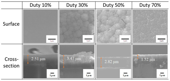
Figure 1.
Surface and cross-sectional SEM images of films fabricated at different duty ratios.
Figure 2 displays the deposition rates calculated from the film thicknesses. The deposition rate increased from a duty cycle of 10% to 30%, reaching a peak of approximately 208 μm/h at 30%. Beyond this duty cycle, the deposition rate declined to 91 μm/h at 70%.
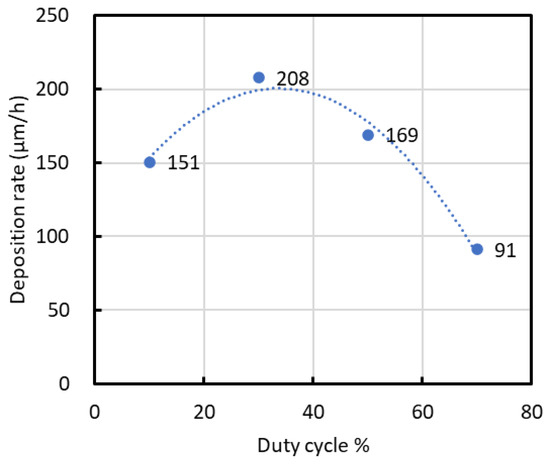
Figure 2.
Deposition rate calculated from film thickness.
Figure 3 outlines the composition of films fabricated at each duty cycle. Carbon was the predominant element, with its highest content at a duty cycle of 10% being 48 at.%. All films contained approximately 20 at.% silicon. Nitrogen content was the lowest at a 10% duty cycle, at 7 at.%, while films deposited at higher duty cycles maintained nitrogen contents of approximately 26 at.%. Oxygen, observed in all samples, was attributed to a natural oxide film formed on the surface upon exposure to the atmosphere after deposition.
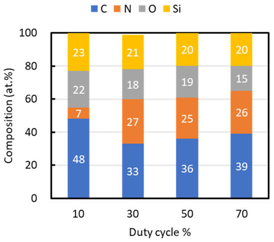
Figure 3.
Composition of films fabricated at different duty ratios.
From the XRD patterns of the films, none of the films showed discernible peaks, confirming their amorphous structure devoid of crystalline forms of SiCN, SiC, Si3N4, or carbon materials such as diamond or graphite. Figure 4 displays the Raman spectra of films fabricated at various duty cycles. No peaks were observed in the wavenumber range of 1000 to 2000 cm−1 at a duty cycle of 10%, indicating the absence of carbon-related structures such as SiC, diamond, graphite, or diamond-like carbon, which typically exhibit peaks in this range. However, at 10% duty cycle, two peaks appeared at 2900 and 2970 cm−1, corresponding to the C–H stretching modes [17], indicating a significant hydrogen content in the film. In contrast, films deposited at duty cycles of 30% to 70% exhibited spectral characteristics of amorphous carbon, with peaks centered around the G (1580 cm−1) and D (1350 cm−1) bands [18]. The background in the spectrum showed a strong slope due to fluorescence at a duty cycle of 30%, which was notably less pronounced at 50% and 70%.
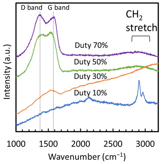
Figure 4.
Raman spectra of films fabricated at different duty ratios.
The spectra obtained at duty cycles of 30% to 70% were deconvoluted into two peaks, the D and G bands, to obtain the ID/IG ratio, G peak position, full width at half maximum (FWHM) of the G peak, and the slope m of the background. Additionally, the m/IG ratio was calculated from the slope m and IG. Figure 5 displays the results for (a) ID/IG ratio, (b) G peak position, (c) FWHM of the G peak, and (d) m/IG in the Raman spectra of films deposited at duty cycles of 30%, 50%, and 70%.
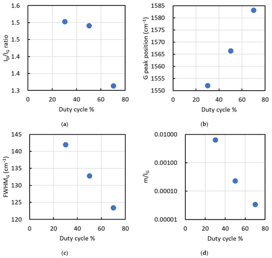
Figure 5.
Results for (a) ID/IG ratio, (b) G peak position, (c) FWHM of the G peak, and (d) m/IG in the Raman spectra of films deposited at duty cycles of 30%, 50%, and 70%.
The ID/IG ratio varied from 1.5 to 1.3, decreasing as the duty cycle increased, particularly between 50% and 70%. Conversely, the G peak position, FWHM of the G peak, and m/IG decreased with increasing duty cycle. The ID/IG ratio and G peak position are inversely correlated with the sp3/sp2 ratio of the carbon structure, where lower values indicate a higher sp3 content [18]. The FWHM of the G peak is indicative of film density, with larger values suggesting higher density [18].
In Si-doped hydrogenated amorphous carbon films, Raman parameters such as the ID/IG ratio, G peak position, and FWHM of the G peak decrease with increasing Si content [19]. Conversely, the G peak position of nitrogen-doped diamond-like carbon (DLC) shifts to higher wavenumbers as the nitrogen content increases [18]. In this study, the Si and N contents of films deposited at duty cycles ranging from 30% to 70% had little effect on the ID/IG ratio, G peak position, and FWHM of the G peak, as these elements remained nearly constant.
From these observations, the ID/IG ratio, G peak position, and FWHM of the G peak changed significantly between duty cycles of 50% and 70%. At 70% duty cycle, the lower ID/IG ratio and FWHM of the G peak, along with a higher G peak position, indicate graphitization and reduced film density due to the elevated deposition conditions. Graphitization here refers to an increase in sp2-bonded carbon clustering/short-range graphitic ordering within an amorphous matrix, not the formation of crystalline graphite detectable by XRD. Conversely, films deposited at a duty cycle of 30% exhibited a higher sp3 ratio and greater film density.
The m/IG ratio decreased with increasing duty cycle, correlating with hydrogen content, where lower values indicate reduced hydrogen incorporation [18]. Moreover, when the empirical relationship developed for a-C:H films [20] is used to convert the m/IG ratio into an apparent hydrogen content, the estimated values fall in the range of approximately 10–17 at.% across the studied duty cycles. However, because this relationship was derived for a-C:H, these values should be regarded as qualitative indicators rather than quantitative hydrogen contents for the present a-SiCN system. Reliable determination of the absolute hydrogen concentration would require a direct method such as ERDA. Nevertheless, the systematic decrease in m/IG with duty cycle suggests that hydrogen incorporation likely changes by on the order of several at.% under the present duty-cycle-controlled deposition conditions.
Figure 6 presents the XPS spectra [(a) Si 2p, (b) C 1s, and (c) N 1s] of films fabricated at different duty ratios, with spectral assignments based on literature data [21,22,23]. The Si 2p spectra [Figure 6a] showed peaks for Si–C (100.8 eV) and Si–N (101.9 eV). In the C 1s spectra [Figure 6b], peaks were observed for Si–C (283.7 eV), C=C (284.5 eV), and C=N (286.1 eV). The N 1s spectra [Figure 6c] displayed peaks for Si–N (397.4 eV) and C=N (398.3 eV).
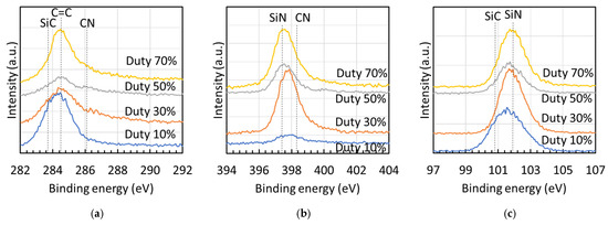
Figure 6.
XPS spectra [(a) Si 2p, (b) C 1s, and (c) N 1s] of deposits fabricated at different duty ratios, illustrating peak area ratios of Si 2p and C 1s spectra.
Figure 7 shows representative load–displacement profiles from the nanoindentation tests for each condition. The average indentation depths at duty ratios of 10, 30, 50, and 70% were 580, 170, 120, and 180 nm, respectively, corresponding to penetration depths of 23.2, 4.8, 4.2, and 12.0% of the film thickness. Substrate effects are commonly considered negligible when the indentation depth is limited to approximately one-tenth to one-eighth of the film thickness; however, for the 10% duty condition, the indentation depth was relatively large, suggesting that the measured mechanical properties may be influenced by the substrate. Figure 8 presents (a) hardness (H) and elastic modulus (E), and (b) the H/E and H3/E2 ratios of the films. Nanoindentation was performed at nine locations per sample, and the results are reported as mean ± standard deviation (n = 9). The hardness values were 1.03 ± 0.06, 12.56 ± 1.80, 22.65 ± 6.78, and 9.20 ± 1.91 GPa for duty ratios of 10%, 30%, 50%, and 70%, respectively. The corresponding Young’s modulus values were 10.14 ± 0.27, 106.63 ± 13.18, 227.57 ± 94.71, and 105.14 ± 12.93 GPa. Both hardness and elastic modulus increased linearly with increasing duty cycle up to 50%, after which they rapidly declined. The peak values for hardness and elastic modulus were observed at a duty cycle of 50%. A similar trend was noted for the H3/E2 ratio. However, the H/E ratio peaked at a duty cycle of 30%, reaching a value of 0.12. The elastic strain to failure (H/E) and the plastic deformation resistance factor (H3/E2) are commonly used to qualitatively assess a material’s resistance to failure [24,25,26]. Previous studies indicate that the H/E ratios for DLC, TiN, and TiAlN range from 0.07 to 0.11, 0.06, and 0.07, respectively, while their H3/E2 values range from 0.15 to 0.45, 0.14, and 0.18, respectively [24,27]. At a duty cycle of 50%, the film exhibited a high H3/E2 ratio, indicative of significant resistance to cracking, whereas at a 30% duty cycle, the film demonstrated a high elastic strain limit due to its high H/E ratio.
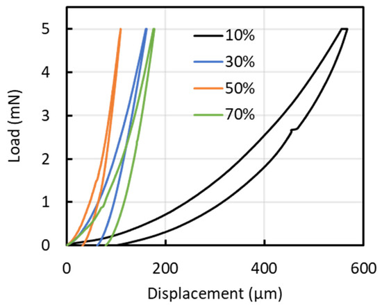
Figure 7.
Representative load–displacement profiles from the nanoindentation tests for each condition.
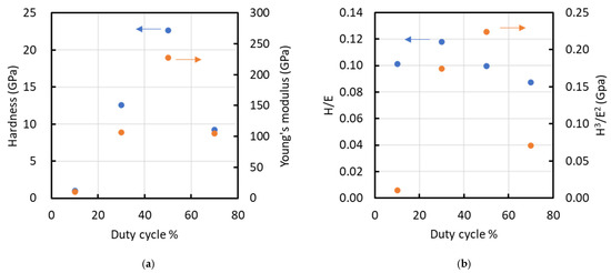
Figure 8.
Relationship between duty cycle and various parameters such as (a) hardness (left y-axis) and Young’s modulus (right y-axis), and (b) H/E (left y-axis) and H³/E² (right y-axis). Arrows indicate the corresponding y-axes.
4. Discussion
In this study, the microwave power was operated in a pulsed mode to generate a pulsed plasma, and the duty ratio was systematically varied. Because the duty ratio affects not only the substrate temperature but also duty-dependent plasma kinetics (e.g., ion flux/energy and radical-related processes), the results are interpreted in terms of effective deposition conditions, in which the measured substrate temperature serves as a practical indicator reflecting coupled thermal effects and plasma–surface interactions (ion bombardment). On this basis, we discuss how the effective deposition conditions govern hydrogen incorporation/desorption, bonding evolution (Si–N, C=N, CN-related bonds), and sp2-rich carbon clustering, thereby determining hardness.
In this study, the microwave power was operated in a pulsed mode, generating a pulsed plasma, and the duty ratio was adjusted to systematically vary the effective deposition conditions, including the substrate temperature. In plasma-enhanced chemical vapor deposition (plasma CVD), pulsed plasma allows plasma generation and gas dissociation to proceed during the on-time, while recombination processes and etching reactions dominate during the off-time. Therefore, by controlling the duty ratio, defined as the ratio of the on-time to the total pulse period, it is possible to regulate both the plasma state and the surface reactions occurring on the substrate.
Shanaghi et al. [28] reported that, even at a constant substrate temperature, controlling the duty ratio resulted in changes in film properties compared with those obtained under continuous plasma conditions. Similarly, Ebrahimi et al. [29] optimized the wear resistance of DLC films by controlling various deposition parameters, including the duty ratio, within a substrate temperature range of 60–150 °C. However, they also noted that it is difficult to completely decouple the effects of duty ratio and substrate temperature.
Likewise, Tanaka et al. [30] reported that, during DLC deposition using a microwave sheath–voltage combination plasma (MVP), variation in the duty ratio resulted in substrate temperatures ranging from 175 °C to 397 °C, and that the deposition rate normalized by the on-time increased with decreasing duty ratio. This behavior was attributed to the dominance of radical deposition during the off-time and the associated increase in hydrogen incorporation into the films.
In the present study, as shown in Figure 9, the deposition rate normalized by the on-time decreases with increasing duty ratio, suggesting that radical deposition during the off-time also occurs under the present conditions. However, in this study, the increase in substrate temperature induced by ion bombardment is as large as approximately 800 °C. This temperature variation is significantly larger than those reported in previous studies. Accordingly, while the individual contributions of duty ratio and temperature cannot be fully separated, the results highlight the dominant role of the combined effective deposition conditions in governing the deposition behavior and film properties.
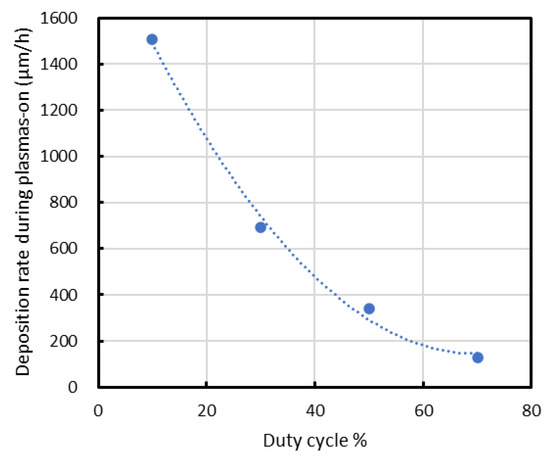
Figure 9.
Deposition rate normalized by the on-time decreases with increasing duty ratio.
From these considerations, the substrate temperature can be regarded as a combined indicator reflecting both the thermal effects that promote surface diffusion and chemical bonding and the flux of ions incident on the substrate, which are intrinsically linked to the duty cycle. Therefore, in the following section, the results are organized using the effective substrate temperature as a practical indicator that reflects both thermal effects and duty-cycle-dependent plasma–surface interactions (e.g., ion bombardment). On this basis, we discuss the apparent relationships between this effective temperature, the evolution of chemical bonding states, and the hardness of the films.
Figure 10 presents the deconvoluted peak–area ratios derived from the XPS spectra shown in Figure 6, including (a) Si 2p, (b) C 1s, and (c) N 1s, for films fabricated at different duty ratios. The predominant peak in the Si 2p spectra of all films was the Si–C bond. When the ion flux to the substrate increased, leading to a higher effective substrate temperature, the ratio of the Si–N bond in the Si 2p spectra monotonically increased. The C=N bond displayed its maximum ratio at 980 °C in both the C 1s and N 1s spectra. Conversely, the C=C bond ratio in the C 1s spectra rapidly decreased between 600 °C and 980 °C, with the predominant peak shifting from C=C to C=N at 980 °C. Thus, films grown under low ion-flux conditions, where the effective substrate temperature did not rise significantly, were primarily composed of Si–C and C=C bonds, while those grown under higher ion-flux conditions featured a mixture of Si–N, Si–C, C=N, and C=C bonds.
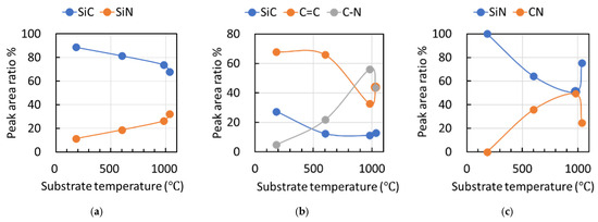
Figure 10.
Presentation of the deconvoluted peak–area ratios derived from the XPS spectra shown in Figure 6, including (a) Si 2p, (b) C 1s, and (c) N 1s, for films fabricated at effective substrate temperatures.
Based on the results shown in Figure 3, Figure 4, Figure 5 and Figure 10, it is evident that amorphous silicon carbon nitride films with different structures, compositions, and bonding states were formed using the MVP method at various effective substrate temperatures.
Specifically, under the low-ion-flux condition at an effective substrate temperature of 180 °C (duty ratio 10%), the deposited film was amorphous silicon carbon nitride with a high hydrogen content. In contrast, under the higher-ion-flux conditions at effective substrate temperatures above ~600 °C (duty ratios ≥ 30%), the hydrogen content decreased, and the combined effects of intense ion bombardment and elevated temperature promoted the incorporation of amorphous carbon-related structures within the films. From these results, it is evident that both the ion flux (plasma–surface interaction intensity) and the substrate temperature (thermal activation) influence the hydrogen incorporation, chemical bonding states, and carbon structure in the films. In addition to radical-driven deposition, increased ion incidence to the substrate under duty-cycle control contributes to the development of film hardness, which reaches a maximum under the condition corresponding to an effective substrate temperature of 980 °C (duty ratio 50%).
At a duty ratio of 10% (low ion flux), the effective substrate temperature rose only to ~180 °C, and the film incorporated hydrogen more readily than nitrogen. This suggests that surface reactions were not sufficiently activated at low temperature, leading to lower hardness due to the high hydrogen content. This interpretation is consistent with the Raman spectrum at a duty ratio of 10%, which exhibited C–H stretching features, indicating the presence of hydrogen-rich bonding configurations in the film. Hydrogen incorporation may reduce film density and promote polymer-like network structures, resulting in lower hardness. These hydrogen-related structural changes could be examined in more detail by analyzing N–H and C–H bonding states using techniques such as FT-IR spectroscopy, which would help clarify the role of hydrogen in determining the mechanical performance under low-temperature deposition conditions.
With increasing duty ratio (and hence increasing effective substrate temperature), hydrogen desorption from the films progressively proceeded. Concurrently, the formation of Si–N and C=N bonds increased, and the C=N bond fraction in the C 1s spectra reached a maximum at duty ratio 50% (effective substrate temperature of 980 °C). Consequently, the maximum hardness was achieved at a duty ratio of 50%. However, when the duty ratio was further increased to 70% and the effective substrate temperature exceeded 1000 °C, the hardness decreased due to enhanced sp2-rich carbon clustering accompanied by a reduction in the C=N bond fraction. This correlation suggests that hydrogen may suppress the formation of CN-related bonding; however, concurrent effects such as thermal rearrangement and the evolution of sp2-rich clustering should also be considered.
Under such high-ion-flux conditions with concomitant high effective temperatures (~1000 °C), CN bonding may become less stable, and partial nitrogen dissociation/desorption could promote the formation of sp2-bonded carbon clustering. In contrast, Si–N bonds are generally more stable at elevated temperatures and are expected to be less sensitive to ion-incidence–induced bond rearrangement. This may explain the monotonic increase in the Si–N bond contribution observed in the Si 2p spectra. As a result, although the overall elemental composition in Figure 3 shows no large change, the bonding configuration can still evolve substantially with temperature, leading to the observed changes in carbon structure and mechanical properties.
In addition, Figure 3 shows that oxygen is detected in all films (up to 22 at.%). Although this oxygen is likely attributable to a naturally formed surface oxide layer after exposure to air, previous studies have also reported the formation of oxide-containing networks (e.g., SiOCN-related bonding), suggesting that oxygen could contribute to Si–O network formation and thereby influence film properties. To clarify the role of oxygen, future work using depth profiling is required. However, Ar sputtering may induce preferential sputtering and chemical modifications, such as apparent changes in Si–C/Si–N bonding and nitrogen loss, which can complicate quantitative interpretation. Therefore, depth-resolved characterization using techniques such as ToF-SIMS will be valuable in future work to determine the oxygen depth distribution and to assess its influence on bonding configuration and mechanical performance.
Figure 11 plots the film hardness as a function of the CN-bond fraction estimated from the deconvoluted N 1s XPS spectra. Although only four data points are available and the scatter is non-negligible, the plot suggests a tentative trend in which higher hardness is associated with a higher CN-bond fraction. In addition, films deposited under conditions that favor higher hydrogen incorporation—as qualitatively indicated by Raman parameters (e.g., m/IG)—tend to show a lower CN-related bonding contribution. However, given the limited number of data points and the indirect nature of the hydrogen estimation, these observations should be regarded as qualitative and do not establish a statistically robust correlation.
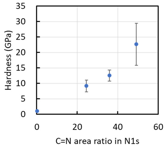
Figure 11.
Hardness of films as a function of the CN bond content determined from their N1s XPS spectra.
In addition, it is worth noting that in our previous MVP-based study [11], a higher hardness of approximately 30 GPa was achieved at a TMS concentration of 20% with a duty cycle of 50%. That work also reported an increasing trend in hardness with increasing TMS concentration. In the present study, the TMS concentration was fixed at 10%, which is lower than the condition that produced the maximum hardness in our previous work. Therefore, the lower peak hardness observed here (~22 GPa) is likely attributable, at least in part, to the reduced TMS concentration, which may limit the attainable bonding configuration (e.g., CN/C=N-related network formation) and/or densification required for achieving higher hardness under MVP deposition conditions.
To further enhance hardness, it is crucial to promote C=N bond formation while suppressing excessive sp2-rich carbon clustering. Increasing nitrogen incorporation is one possible route; however, controlling the resulting bonding configuration remains challenging. In practical applications, high-temperature deposition also restricts the choice of substrates (e.g., steels). Based on the present results, increasing the duty cycle likely enhances ion bombardment to the substrate, leading to a higher effective substrate temperature and promoting C=N bond formation, which together contribute to increased hardness. Therefore, if a deposition mode enabling high ion flux/ion energy at low duty cycle (i.e., low average thermal load) can be realized—e.g., by generating a higher-density plasma and/or applying additional substrate bias or sheath control—simultaneous low-temperature deposition and high hardness may be achievable by facilitating hydrogen removal and CN-bond formation without excessive heating.
5. Conclusions
In this study, amorphous silicon carbon nitride (a-SiCN) films were synthesized by microwave plasma-enhanced chemical vapor deposition using a microwave sheath–voltage combination plasma (MVP) source. The microwave duty ratio was varied from 10% to 70%, which increased the substrate temperature from approximately 180 °C to 1040 °C.
The duty-cycle-controlled deposition conditions—accompanied by coupled changes in substrate temperature and plasma–surface interaction intensity—strongly affected the deposition behavior, atomic composition, chemical bonding states, carbon structure, and mechanical properties of the films.
At a low duty ratio of 10% (low thermal load/low substrate temperature), the films showed substantial hydrogen incorporation and were dominated by CH- and Si–C-related bonding with a comparatively low nitrogen content. With increasing duty ratio, hydrogen incorporation decreased, carbon content was reduced, and the contributions of Si–N and C=N bonding increased. These trends are consistent with the Raman analysis showing a decrease in the ID/IG ratio, indicating progressive hydrogen desorption under more severe effective deposition conditions.
The hardness increased as the duty ratio was raised from 10% to 50%, reaching a maximum of ~22 GPa at 50% (≈980 °C). This increase coincided with an increased CN-bond contribution, suggesting that enhanced C=N bonding is associated with strengthening of the a-SiCN network under the present conditions. In contrast, at 70% (≈1040 °C), the hardness decreased to ~9 GPa, accompanied by the development of sp2-rich carbon clustering (graphite-like short-range ordering) and a reduced CN-bond fraction.
Overall, these results indicate that the effective substrate temperature—reflecting both thermal effects and duty-cycle-dependent plasma–surface interactions—can be used as a practical indicator to interpret hydrogen desorption, bonding evolution, and hardness changes in the investigated a-SiCN films. The findings underscore the importance of optimizing duty-cycle-controlled deposition conditions to promote CN-bond formation while suppressing excessive sp2 clustering.
Finally, based on the observed correlations, we propose that achieving high ion flux/energy at a low duty ratio (i.e., low average thermal load)—for example, by increasing plasma density and/or applying an additional substrate bias—may be a promising route for future work toward simultaneously low-temperature deposition and high hardness through enhanced hydrogen removal and CN-bond formation.
Author Contributions
Conceptualization, I.T.; methodology, I.T.; validation, I.T. and Y.H. (Yuki Hatae); formal analysis, I.T. and Y.H. (Yuki Hatae); investigation, I.T. and Y.H. (Yuki Hatae); resources, I.T.; data curation, I.T.; writing—original draft preparation, I.T. and Y.H. (Yuki Hatae); writing—review and editing, I.T.; visualization, I.T. and Y.H. (Yuki Hatae); supervision, Y.H. (Yasunori Harada); project administration, I.T.; funding acquisition, I.T. All authors have read and agreed to the published version of the manuscript.
Funding
This work was partially supported by the Japan Society for the Promotion of Science (JSPS) through KAKENHI (Grant Numbers 21K14440 and 24K08100), and by the Iketani Science and Technology Foundation, Japan.
Data Availability Statement
The original contributions presented in this study are included in the article material. Further inquiries can be directed to the corresponding author.
Conflicts of Interest
The authors declare no conflicts of interest.
References
- Mishra, S.K.; Verma, D.; Bysakh, S.; Pathak, L.C. Hard and soft multilayered SiCN nanocoatings with high hardness and toughness. J. Nanomater. 2013, 2013, 949416. [Google Scholar] [CrossRef]
- Zhang, D.H.; Gao, Y.; Wei, J.; Mo, Z.Q. Influence of silane partial pressure on the properties of amorphous SiCN films prepared by ECR-CVD. Thin Solid Films 2000, 377, 607–610. [Google Scholar] [CrossRef]
- Kozak, A.O.; Ivashchenko, V.I.; Porada, O.K.; Ivashchenko, L.A.; Tomila, T.V.; Manjara, V.S.; Klishevych, G.V. Structural, optoelectronic and mechanical properties of PECVD Si–C–N films: An effect of substrate bias. Mater. Sci. Semicond. Process. 2018, 88, 65–72. [Google Scholar] [CrossRef]
- Bhattacharyya, A.S.; Mishra, S.K.; Mukherjee, S. Correlation of structure and hardness of RF magnetron sputtered silicon carbonitride films. J. Vac. Sci. Technol. A 2010, 28, 505–509. [Google Scholar] [CrossRef]
- Gao, P.; Xu, J.; Piao, Y.; Ding, W.; Wang, D.; Deng, X.; Dong, C. Deposition of silicon carbon nitride thin films by microwave ECR plasma enhanced unbalance magnetron sputtering. Surf. Coat. Technol. 2007, 201, 5298–5301. [Google Scholar] [CrossRef]
- Zhou, F.; Yue, B.; Wang, X.; Wu, X.; Zhuge, L. Surface roughness, mechanical properties and bonding structure of silicon carbon nitride films grown by dual ion beam sputtering. J. Alloys Compd. 2010, 492, 269–276. [Google Scholar] [CrossRef]
- Probst, D.; Hoche, H.; Zhou, Y.; Hauser, R.; Stelzner, T.; Scheerer, T.; Broszeit, E.; Berger, C.; Riedel, R.; Stafast, H.; et al. Development of PE-CVD Si/C/N:H films for tribological and corrosive complex-load conditions. Surf. Coat. Technol. 2005, 200, 355–359. [Google Scholar] [CrossRef]
- Ma, S.; Xu, B.; Wu, G.; Wang, Y.; Ma, F.; Ma, D.; Xu, K.; Bell, T. Microstructure and mechanical properties of SiCN hard films deposited by an arc enhanced magnetic sputtering hybrid system. Surf. Coat. Technol. 2008, 202, 5379–5382. [Google Scholar] [CrossRef]
- Shi, Z.; Wang, Y.; Du, C.; Huang, N.; Wang, L.; Ning, C. The structure, surface topography and mechanical properties of Si–C–N films fabricated by RF and DC magnetron sputtering. Appl. Surf. Sci. 2011, 258, 1328–1336. [Google Scholar] [CrossRef]
- Ji, C.; Cai, X.; Zhou, Z.; Gao, B.; Liu, S. Effects of atomic ratio on the mechanical properties of amorphous silicon carbon nitride. Materials 2022, 15, 6865. [Google Scholar] [CrossRef]
- Tanaka, I.; Hatae, Y.; Harada, Y. The deposition of amorphous silicon carbon nitride films using high-density plasma CVD. In Proceedings of the International Tribology Conference (ITC), Fukuoka, Japan, 25–30 September 2023; pp. 28-PO–40. [Google Scholar]
- Xu, J.; Kousaka, H.; Umehara, N.; Diao, D. Plasma properties of a new surface-wave-sustained plasma source under the conditions of depositing DLC films. Surf. Coat. Technol. 2006, 201, 408–412. [Google Scholar] [CrossRef]
- Kousaka, H.; Umehara, N.; Ono, K.; Xu, J. Microwave-excited high-density plasma column sustained along metal rod at negative voltage. Jpn. J. Appl. Phys. 2005, 44, 1154–1157. [Google Scholar] [CrossRef]
- Cha, J.-H.; Seo, K.-S.; Kim, S.-W.; Lee, H.-J. Two-dimensional fluid simulation of inductively coupled N2/NH3/SiH4 discharge. J. Phys. D Appl. Phys. 2022, 55, 035203. [Google Scholar] [CrossRef]
- Saifutdinov, A.; Kustova, E. Simulation of filamentation dynamics of microwave discharge in nitrogen. Plasma Sources Sci. Technol. 2023, 32, 125010. [Google Scholar] [CrossRef]
- Tanaka, I.; Okubo, H.; Harada, Y. Diamond synthesis on Si by plasma chemical vapor deposition using microwave sheath-voltage combination plasma. Surf. Coat. Technol. 2021, 423, 127592. [Google Scholar] [CrossRef]
- Zou, J.W.; Schmidt, K.; Reichelt, K.; Dischler, B. The properties of a-C:H films deposited by plasma decomposition of C2H2. J. Appl. Phys. 1990, 67, 487–494. [Google Scholar] [CrossRef]
- Ferrari, A.C.; Robertson, J. Raman spectroscopy of amorphous, nanostructured, diamond-like carbon, and nanodiamond. Philos. Trans. R. Soc. A 2004, 362, 2477–2512. [Google Scholar] [CrossRef]
- Ong, S.E.; Zhang, S.; Du, H.; Sun, D. Relationship between bonding structure and mechanical properties of amorphous carbon containing silicon. Diam. Relat. Mater. 2007, 16, 1628–1635. [Google Scholar] [CrossRef]
- Choi, J.; Ishii, K.; Kato, T.; Kawaguchi, M. Evaluation and prediction of mechanical properties of DLC films by Raman spectroscopy (Part 1)—DLC films prepared by bipolar PBII&D with a source gas of toluene. J. Jpn. Soc. Tribol. 2013, 58, 596–602. [Google Scholar]
- Ivashchenko, V.I.; Porada, O.K.; Ivashchenko, L.A.; Timofeeva, I.I.; Sinel’Nichenko, O.K.; Butenko, O.O.; Ushakov, M.V.; Ushakova, L.A. Characteristics of thin plasmachemical silicon carbon nitride films deposited using hexamethyldisilane. Powder Metall. Met. Ceram. 2009, 48, 66–72. [Google Scholar] [CrossRef]
- Mitu, B.; Dinescu, G.; Budianu, E.; Ferrari, A.; Balucani, M.; Lamedica, G.; Dauscher, A.; Dinescu, M. Formation of intermediate SiCN interlayer during deposition of CNx on a-Si:H or a-SiC:H thin films. Appl. Surf. Sci. 2001, 184, 96–100. [Google Scholar] [CrossRef]
- Chen, C.W.; Huang, C.C.; Lin, Y.Y.; Chen, L.C.; Chen, K.H. The affinity of Si–N and Si–C bonding in amorphous silicon carbon nitride (a-SiCN) thin film. Diam. Relat. Mater. 2005, 14, 1126–1130. [Google Scholar] [CrossRef]
- Bartosik, M.; Rumeau, C.; Hahn, R.; Zhang, Z.L.; Mayrhofer, P.H. Fracture toughness and structural evolution in the TiAlN system upon annealing. Sci. Rep. 2017, 7, 16476. [Google Scholar] [CrossRef] [PubMed]
- Leyland, A.; Matthews, A. On the significance of the H/E ratio in wear control: A nanocomposite coating approach to optimised tribological behaviour. Wear 2000, 246, 1–11. [Google Scholar] [CrossRef]
- Musil, J.; Jirout, M. Toughness of hard nanostructured ceramic thin films. Surf. Coat. Technol. 2007, 201, 5148–5152. [Google Scholar] [CrossRef]
- Panwar, O.S.; Tripathi, R.K.; Chockalingam, S. Improved nanomechanical properties of hydrogenated tetrahedral amorphous carbon films measured with ultra-low indentation load. Mater. Express 2015, 5, 410–418. [Google Scholar] [CrossRef]
- Shanaghi, A.; Sabour Rouhaghdam, A.R.; Ahangarani, S.; Chu, P.K.; Shahrabi Farahani, T. Effects of duty cycle on microstructure and corrosion behavior of TiC coatings prepared by DC pulsed plasma CVD. Appl. Surf. Sci. 2012, 258, 3051–3057. [Google Scholar] [CrossRef]
- Ebrahimi, M.; Mahboubi, F.; Naimi-Jamal, M.R. Optimization of pulsed DC PACVD parameters: Toward reducing wear rate of the DLC films. Appl. Surf. Sci. 2016, 389, 521–531. [Google Scholar] [CrossRef]
- Tanaka, I.; Ikeda, T.; Nakano, T.; Kousaka, H.; Furuki, T. Effect of humidity on the friction properties of a-C:H and a-C:H:Si films deposited by PECVD employing microwave sheath–voltage combination plasma. Jpn. J. Appl. Phys. 2019, 58, SAAC06. [Google Scholar] [CrossRef]


Disclaimer/Publisher’s Note: The statements, opinions and data contained in all publications are solely those of the individual author(s) and contributor(s) and not of MDPI and/or the editor(s). MDPI and/or the editor(s) disclaim responsibility for any injury to people or property resulting from any ideas, methods, instructions or products referred to in the content. |
© 2026 by the authors. Licensee MDPI, Basel, Switzerland. This article is an open access article distributed under the terms and conditions of the Creative Commons Attribution (CC BY) license.