Letter

Electrochromic Performance of V2O5 Thin Films Grown by Spray Pyrolysis

1
Center of Materials Technology and Photonics, School of Engineering, Hellenic Mediterranean University, 71410 Heraklion, Greece
2
Department of Physics, University of Patras, 26500 Patras, Greece
3
Department of Chemistry, University of Crete, 70013 Heraklion, Greece
4
National Institute for Research and Development in Microtechnologies—IMT Bucharest, 126A, Erou Iancu 8 Nicolae Street, 077190 Bucharest, Romania
5
Department of Electrical and Computer Engineering, School of Engineering, Hellenic Mediterranean University, 71410 Heraklion, Greece
*
Authors to whom correspondence should be addressed.
Materials 2020, 13(17), 3859; https://doi.org/10.3390/ma13173859
Submission received: 5 August 2020 / Revised: 26 August 2020 / Accepted: 29 August 2020 / Published: 1 September 2020
(This article belongs to the Special Issue Advances in Chemical Vapor Deposition)

Abstract

:
A new approach regarding the development of nanostructured V2O5 electrochromic thin films at low temperature (250 °C), using air-carrier spray deposition and ammonium metavanadate in water as precursor is presented. The obtained V2O5 films were characterized by X-ray diffraction, scanning electron microscopy and Raman spectroscopy, while their electrochromic response was studied using UV-vis absorption spectroscopy and cyclic voltammetry. The study showed that this simple, cost effective, suitable for large area deposition method can lead to V2O5 films with large active surface for electrochromic applications.

1. Introduction

Currently, many efforts are going on worldwide to develop new electrochromic materials for energy and environmental applications. V2O5 compounds keep attracting much attention because of their structural flexibility and chemical/physical properties, which are suitable for catalytic and electrochemical applications [1,2,3]. The layered structure with orthorhombic symmetry of α-V2O5 can be well adapted to the reversible incorporation of guest Li+ ions. As a result, its films have been recognized as the most attractive material for applications in electrochromic devices and in lithium batteries [3,4,5,6,7,8,9,10,11]. The valence state of V atoms is known to be extremely sensitive to the chemical environment, a behavior that can lead to a variety of structures containing different building units and exhibiting different physical properties. In particular, the structure and the morphology of vanadium oxide films are intimately related to the deposition method and the operating conditions. Moreover, since the direct growth of crystalline V2O5 films is very difficult except in the cases of some sub-stoichiometric oxides, annealing of the as-prepared films might be required in order to improve properties and functionality. Over the years, many techniques were involved for the deposition of V2O5 thin films for electrochromic applications, including electrodeposition, sputtering, sol-gel, hydrothermal growth and doctor-blade [12,13,14,15,16]. Some trials have been also reported on the use of spray pyrolysis for the deposition of large surfaces electrochromic V2O5 films, most of them using relatively high temperatures (>500 °C) vanadium chloride (i.e., moisture sensitive and toxic), vanadium nitride (i.e., irritant) as precursors [17,18,19,20].
The present letter concerns preliminary results on a new approach for developing nanostructured V2O5 thin films for electrochromic applications. In particular, air-carrier spray deposition at quite low temperature has been employed with ammonium metavanadate dissolved in water, which is a rather simple and low-cost precursor.

2. Materials and Methods

2.1. Materials

Ammonium metavanadate, ACS reagent, ≥99.0% (NH4VO3) was purchased from Sigma-Aldrich (St. Louis, MO, USA) and distilled water was used as a solvent for the precursor’s preparation. Lithium perchlorate, ACS reagent, ≥95.0% (LiCLO4) from Sigma-Aldrich was used as electrolyte and propylene carbonate, anhydrous, 99.7% from Sigma-Aldrich was the electrolyte’s solvent. Finally, fluorine-doped tin Oxide (FTO–SnO2:F) coated glass was the substrate.

2.2. Preparation of V2O5 Samples

A custom-made spray pyrolysis technique was utilized for the preparation of the samples. The deposition was carried out at a distance of 30 cm between the spray gun and the substrate, which was kept at a temperature of 250 °C. The precursor solution was prepared by dissolving the required amount of ammonium metavanadate (NH4VO3) in distilled water. Two concentrations were used, 0.01 M and 0.02 M. Since the optical difference between the colored and the bleached states of the as deposited samples was very low as well as their electrochromic performance was quite poor, thermal annealing was carried out for 2 h at 400 °C in oxygen atmosphere. More details regarding the sample names and the growth parameters can be found in Table 1. The respective thickness was measured to be about a micron.

2.3. Structural and Morphological Characterization

X-ray diffraction (XRD), scanning electron microscopy (SEM) and Raman Spectroscopy were used to analyze the structure and the morphology of the deposited V2O5 films. For the XRD measurements, a 9kW SmartLab X-ray Diffraction System (Rigaku, Tokyo, Japan) was employed, with rotating anode that employs Cu Kα1 radiation (λ = 1.5406 Å) in parallel-beam mode. To reveal the crystalline structure of the layer, the grazing incidence technique was used, the incidence angle was kept at 0.5°, while the detector was moved from 5 to 95°. SEM characterization was performed using a Nova NanoSEM 630 (FEI Company, Hillsborough, OR, USA), field emission scanning electron microscope for the annealed samples so that a better resolution and insight on their fine surface structuring can be obtained. All samples were characterized in high vacuum mode without any coating. Raman spectroscopy was performed at room temperature using a WiTec Raman spectrometer (Alpha-SNOM 300 S, WiTec GmbH, Ulm, Germany) using 532 nm excitation, from a diode-pumped solid-state laser with a maximum power of 145 mW. The incident laser beam with a spot-size of about 1.0 µm was focused onto the sample with a 100× long working distance microscope objective. The Raman spectra were collected with an exposure time of 20 s accumulation and the scattered light was collected by the same objective in back-scattering geometry using a 600 grooves/mm grating. The spectrometer scanning data collection and processing were carried out using the WiTec Project Five software (Version, WiTec GmbH, Ulm, Germany).

2.4. Electrochemical Characterization

Electrochemical experiments were performed using a PGSTAT302N Autolab (Metrohm AG, Herisau, Switzerland) potentiostat/galvanostat in a three-electrode cell setup, the working electrode with the V2O5 layer on the FTO substrate, the Pt counter electrode and the reference electrode (Ag/AgCl) utilizing 1M, LiClO4 in propylene carbonate as electrolyte [21].

2.5. Optical Characterization

The optical properties of the samples were evaluated by UV-Vis transmittance spectra recorded with a UV-2401PC spectrophotometer (Shimadzu Corporation, Kyoto, Japan,), at a wavelength range of 200 nm to 1000 nm.

3. Results and Discussion

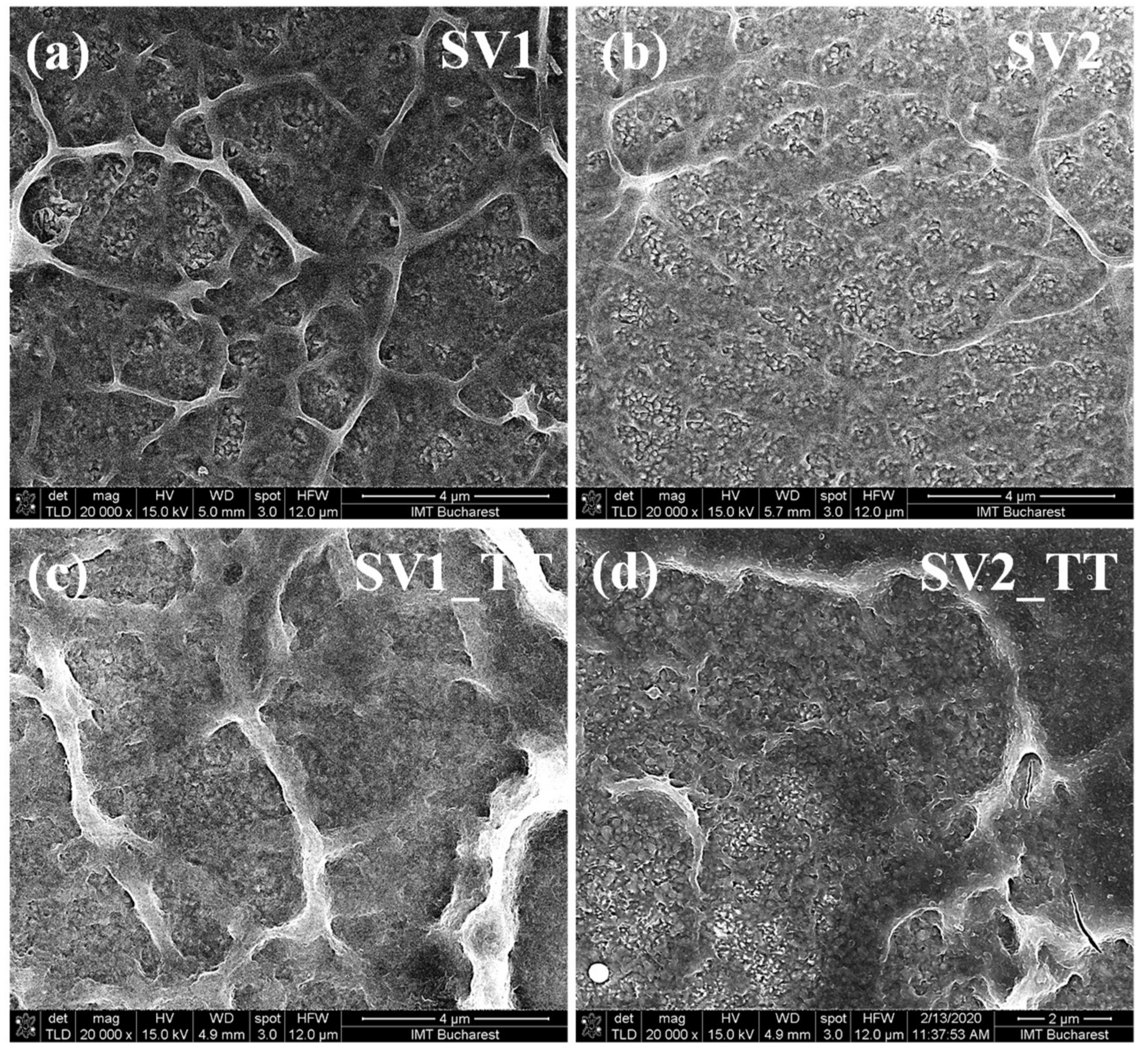
3.1. Morphological Characterization

As shown in Figure 1a,b, SEM characterization revealed the formation of mixed nanostructured granular and wall-like structures films, homogeneously distributed over the film surface.
Moreover, as can be observed, the films present a very large active surface when compared with usual flat granular structured films. Annealing of the films for 2 h at 400 °C in an oxygen atmosphere was found to lead to a decrease of the number of film surface features, as can be seen in Figure 1c,d. This kind of structuring has not been reported before when using other growth techniques and it seems to be directly related to the growth technique used in our work. The particular surface structuring and morphology makes these films suitable for applications that require a high surface to volume ratio.

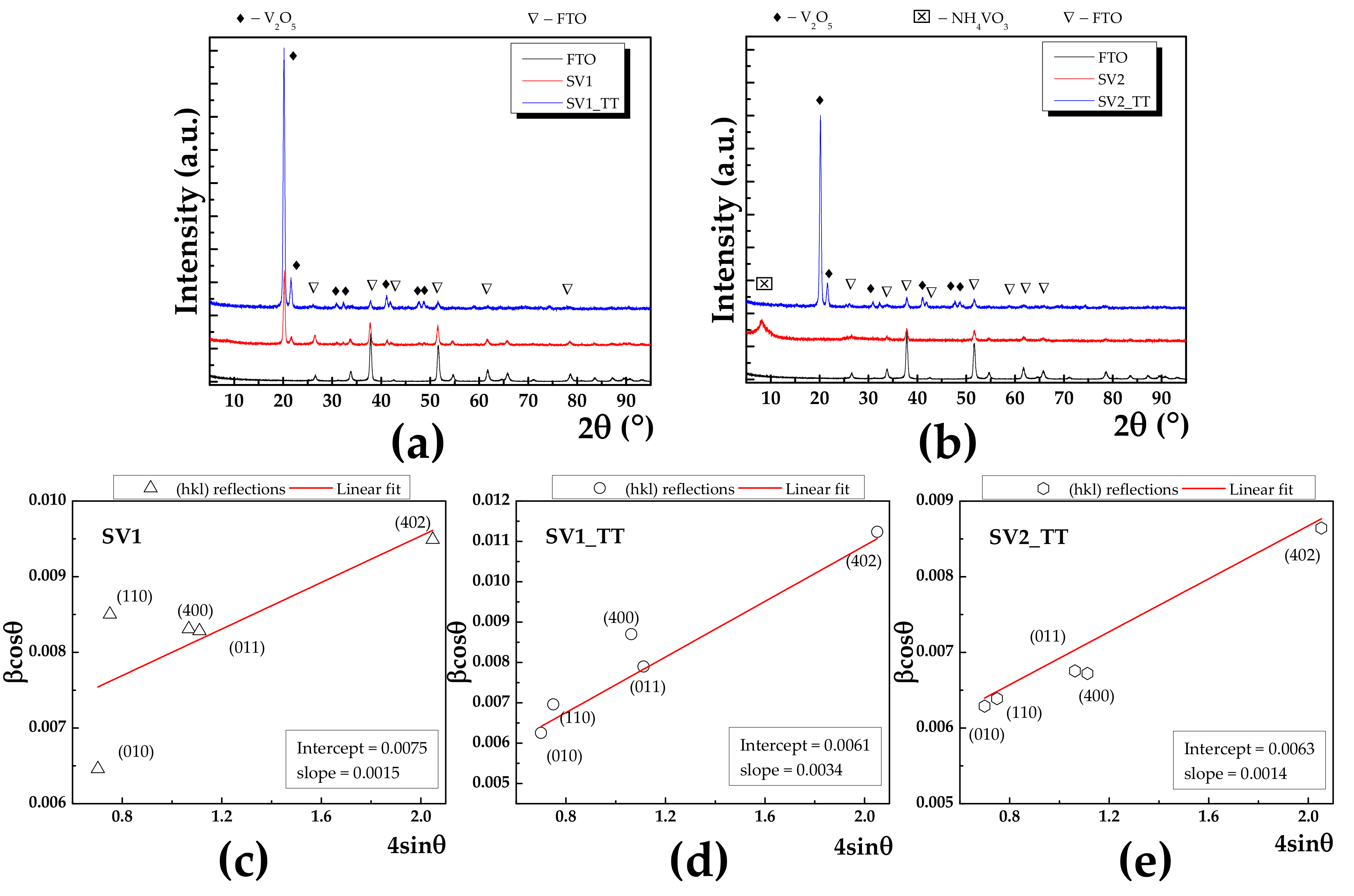
3.2. X-ray Diffraction Analysis

Grazing incidence X-ray diffraction (GIXRD) was used to reveal the crystalline structure of the investigated samples. Since GIXRD requires small incident angles for the incoming X-rays, the diffraction is surface sensitive, the wave penetration being limited, and this approach is used for the study surfaces and layers. Figure 2a shows the GIXRD patterns of SV1 and SV2 before (red line) and after annealing (blue line).
In addition, the corresponding GIXRD pattern of the FTO substrate was also added (black line). The peak indexing was made using International Center for Diffraction Database (ICDD) database. In the case of SV1, the presence of the V2O5 phase was identified, with orthorhombic lattice having parameters a = 11.7 , b = 4.40 and c = 3.45 , while α = β = γ = 90°, which belongs to the 47:Pmmm space group. To gain a thoroughly view of the crystalline features of our materials, we employed Williamson-Hall method, which allowed us to separate the strain and size effects from the Bragg peak. The formalism behind this method can be found in [22]. Figure 2c–e present the Williamson-Hall plots (red line) for SV1, SV1_TT and SV2_TT with corresponding intercept and slope values as inset, which are related to the mean crystallite size and lattice strain, respectively. As a result, the mean crystallite size was increasing from 18.4 to 22.7 nm. For the respective as deposited SV2 sample, the XRD pattern exhibited only a broad peak at 8.07°, which can be attributed to the non-reacted precursor NH4VO3 since it cannot be matched with any vanadium oxide phase. After annealing, the occurrence of V2O5 was visible and the respective mean crystallite size calculated to be 22.1 nm. At the same time, after the annealing process, the lattice strain ε increases from 0.15% (e.g., SV1) to 0.34% (e.g., SV1_TT), which indicates a slight expansion of the interplanar distance. The XRD results indicate that annealing can result in two main effects.
Firstly, the crystallinity is enhanced, which leads to a smaller dislocation density, whose occurrence is due to the boundaries of the adjacent mosaic blocks [23]. Simultaneously, the decreasing of dislocation density is accompanied by a slight expansion of the lattice strain. Secondly, the full conversion from NH4VO3 to V2O5 phase can take place.

3.3. Raman Analysis

Since the structure of α-V2O5 (orthorhombic) belongs to the Pmmn space group [24,25], the V2O5 layers are formed from packing of edge shared VO5 square pyramids linked in the ‘ΧΥ’ plane. Group theoretical analysis predicts twenty-one Raman active modes for V2O5 at Γ point, 7Ag + 7B2g + 3B1g + 4B3g [26,27]. In our case we observed five Raman modes for the annealed films as shown in Figure 3, which match with the reported data for V2O5.
In particular, the Raman peaks we observed were at 138, 280, 522, 691 and 994 cm−1, confirming the presence of α-V2O5 phase [26], as was already identified with XRD. The 5 observed Raman peaks can be assigned as follows:
(a)
The highest frequency peak at 994 cm−1 appears to be due to the stretching vibrational mode of V–OI bond along Z direction.
(b)
Displacement of OIII atoms in Y and X directions generates Raman modes at 691 cm−1 (V–OIII–V antiphase stretching mode) and 522 cm−1 (d4 stretching vibration), respectively.
(c)
Mode 280 cm−1 can be attributed to oscillation of OI atoms along Y axis.
(d)
The low frequency mode at 138 cm−1 corresponds to Y displacement of the whole chain involving shear and rotations of the ladder like V–OIII bonds. The high intensity of 138 cm−1 peak indicates the long range order of V–O layers in the XY plane.
Considering the annealing effect on the film structuring, the most affected modes by the temperature were found to be the V+2=O stretching bands situated at 138 cm−1 which has a slight deviation to the left and the V+3=O situated at 522 cm−1 which increases in Raman intensity. The other V2O5 vibration modes (V+3=O stretching modes situated at 691 cm−1 and V+5=O stretching modes situated at 994 cm−1) were not affected by the compressive stress introduced by temperature [28]. Supplementary peaks associated to nonreacted metavanadate precursor, were detected at 871 cm−1 in the SV2 current study.

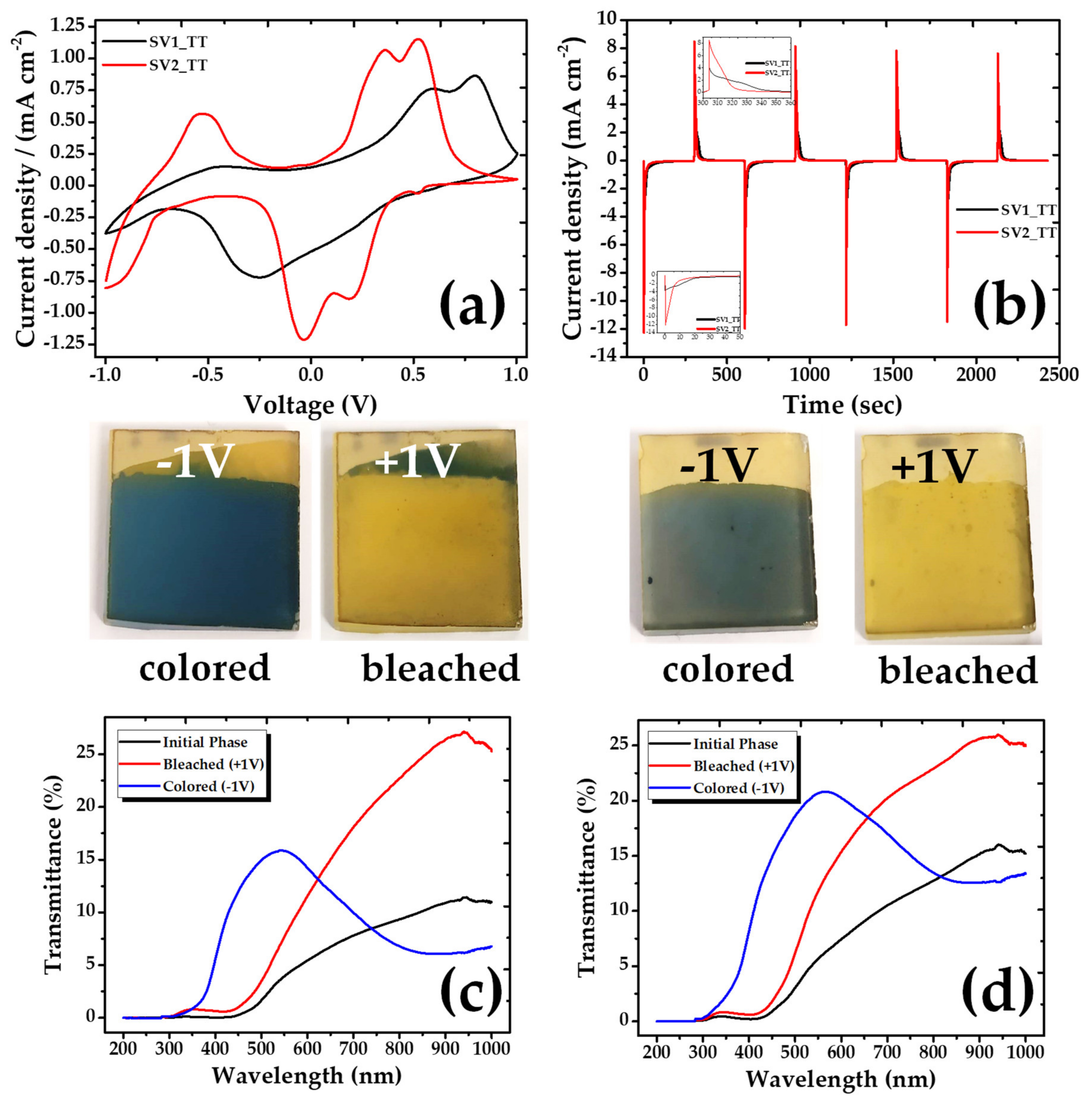
3.4. Electrochemical Characterization

The electrochemical performance of the samples was studied in a three-electrode cell, by cycling the potential between −1 V and +1 V at a scan rate of 10 mV s−1 and using 1M, LiClO4 in propylene carbonate as electrolyte (Figure 4a).
In parallel, their electrochromic performance was studied with UV-Vis absorption spectroscopy. A minimal optical difference between colored and bleached states of the as deposited samples along with poor electrochromic properties were indicated. In particular, the color varied between light gray/yellow (−1 V) and light yellow (+1 V). In order to improve the structure of the V2O5 films and their subsequent performance, the samples were annealed by heating them in an oven at a temperature of 400 °C for 2 h in an oxygen atmosphere. After annealing, the color states changed and improved dramatically, being blue for the SV1 sample and a darker gray for the respective SV2, as compared to the original colors before the annealing process. Comparing the bleached states, the annealed samples have stronger yellow tint than the samples before the annealing. The color changes of the annealed samples are presented in Figure 4.
The SV2_TT coating indicates three cathodic peaks at −0.926 V/−0.010 V/+0.230 V and three anodic peaks at −0.634 V/+0.328 V/+0.485 V, which are attributed to Li+ intercalation and deintercalation accompanying gain and loss of an e. The current density of the particular sample is the highest indicating an enhanced electrochemical activity. On the other hand, the curve of SV1_TT is different showing two anodic and one cathodic peak (Figure 4a). This discrepancy may be related to the expansion of the interplanar distance of SV2_TT, which allows accommodating a greater number of Li ions.
Chronoamperometry measurements were used to evaluate the time evolution of the coloring/bleaching processes (Figure 4b). When a negative voltage (−1.0 V) was applied, the color of the V2O5 coating changed from yellow to blue (SV1_TT sample) or dark grey (SV2_TT sample). With the opposite applied voltage (+1.0 V), the film returned to its initial state, becoming yellow again. From the I–t measurements, the time responses for coloration of the SV1_TT and SV2_TT samples were found to be 34.8 s and 9.8 s, respectively, the respective times for bleaching being 34.2 s and 15.7 s. As can be observed, SV2_TT has a much faster response. The charge densities of these samples, calculated by integrating the current density, were found to be −73.3/−71.01 and 70.7/70.9 mC cm−2 for the SV1_TT and SV2_TT samples, respectively.
The transmittance measurements performed in the annealed samples are also shown in Figure 4c, d. In these graphs, we can observe how the transmittance spectra change between the colored and the bleached state according to the applied voltages in the samples. More specifically, it is obvious that above 650 nm, the color difference is increasing, a behavior indicating that the electrochromic performance of our samples is maximized at the near infrared spectral region.
Finally, the coloration efficiency (CE) factor, defined as the change in optical density (ΔOD) per unit of charge density (Q), was calculated according to the following Equation (1):
C E ( λ ) = Δ O D ( λ ) Q
where ΔOD is the optical density, showing the change in the transmission between the bleached and colored states of the film, that is, Equation (2):
Δ O D ( λ ) = ln T b T c
where, Tb and Tc are the transmittances at bleached and colored state, respectively. Q is the charge density and λ denotes certain wavelengths, which, for our calculations, were taken at 700 and 900 nm. The CE for our films was calculated to be 8.1 and 2.4 cm−2 C−1 for SV1_TT and SV2_TT respectively at 700 nm, increasing up to 20 and 10 cm−2 C−1 at 900 nm. Although the coloration efficiency is higher for the SV1_TT sample, the experiments showed that this is decaying faster than the SV2_TT one, which is presenting better crystalline properties. Since these are preliminary result, further efforts are currently under way in order to increase both the coloration efficiency and the stability of the films.

4. Conclusions

Electrochromic nanostructured V2O5 thin films were prepared at low temperature (250 °C) using air-carrier spray deposition, starting from ammonium metavanadate precursor in water. The obtained V2O5 films were characterized by X-ray diffraction, scanning electron microscopy and Raman spectroscopy, while their electrochromic behavior was studied using UV-vis absorption spectroscopy and cyclic voltammetry. This preliminary study showed that this simple, cost effective, suitable for large area deposition method can lead to novel surface structuring of V2O5 films with electrochromic performance. Further studies for growth optimization and improvements of film properties and stability would be performed.

Author Contributions

Conceptualization, K.E., S.C. and M.S.; methodology, V.T., M.S. and D.V.; validation, K.M., K.E. and M.S.; formal analysis, K.M., V.T. and M.S.; investigation, C.R., O.T., C.P. and K.M.; data curation, K.M., V.T., M.S. and D.V.; writing—original draft preparation K.M., C.R., C.P. and M.S.; writing—review and editing K.M., M.S. and K.E.; supervision, K.E., S.C. and M.S.; project administration, K.E.; funding acquisition, K.M. and K.E. All authors have read and agreed to the published version of the manuscript.

Funding

This research is co-financed by Greece and the European Union (European Social Fund—ESF) through the Operational Program “Human Resources Development, Education and Lifelong Learning” in the context of the project “Strengthening Human Resources Research Potential via Doctorate Research—2nd Cycle” (MIS-5000432), implemented by the State Scholarships Foundation (ΙΚΥ).

Acknowledgments

M.S. involvement was partially supported by the Romanian Ministry of Research and Innovation through Institutional Performance—Projects for Excellence Financing in RDI, Contract no. 13 PFE/16.10.2018.

Conflicts of Interest

The authors declare no conflict of interest.

References

  1. Weckhuysen, B.M.; Keller, D.E. Chemistry, Spectroscopy and the Role of Supported Vanadium Oxides in Heterogeneous Catalysis. Catal. Today 2003, 78, 25–46. [Google Scholar] [CrossRef] [Green Version]
  2. Chernova, N.A.; Roppolo, M.; Dillon, A.C.; Whittingham, M.S. Layered Vanadium and Molybdenum Oxides: Batteries and Electrochromics. J. Mater. Chem. 2009, 19, 2526–2552. [Google Scholar] [CrossRef]
  3. Delmas, C.; Cognac-Auradou, H.; Cocciantelli, J.M.; Ménétrier, M.; Doumerc, J.P. The LixV2O5 System: An Overview of the Structure Modifications Induced by the Lithium Intercalation. Solid State Ion. 1994, 69, 257–264. [Google Scholar] [CrossRef]
  4. Whittingham, M.S. Lithium Batteries and Cathode Materials. Chem. Rev. 2004, 104, 4271–4302. [Google Scholar] [CrossRef]
  5. Whittingham, M.S.; Savinell, R.F.; Zawodzinski, T. Introduction: Batteries and Fuel Cells. Chem. Rev. 2004, 104, 4243–4244. [Google Scholar] [CrossRef] [Green Version]
  6. Murphy, D.W.; Christian, P.A.; DiSalvo, F.J.; Waszczak, J.V. Lithium Incorporation by Vanadium Pentoxide. Inorg. Chem. 1979, 18, 2800–2803. [Google Scholar] [CrossRef]
  7. Whittingham, M.S. The Role of Ternary Phases in Cathode Reactions. J. Electrochem. Soc. 1976, 123, 315. [Google Scholar] [CrossRef]
  8. Wiesener, K.; Schneider, W.; Ilić, D.; Steger, E.; Hallmeier, K.H.; Brackmann, E. Vanadium Oxides in Electrodes for Rechargeable Lithium Cells. J. Power Sources 1987, 20, 157–164. [Google Scholar] [CrossRef]
  9. Mukherjee, A.; Ardakani, H.A.; Yi, T.; Cabana, J.; Shahbazian-Yassar, R.; Klie, R.F. Direct Characterization of the Li Intercalation Mechanism into α-V2O5 Nanowires Using in-Situ Transmission Electron Microscopy. Appl. Phys. Lett. 2017, 110, 213903. [Google Scholar] [CrossRef]
  10. Li, H.; He, P.; Wang, Y.; Hosono, E.; Zhou, H. High-Surface Vanadium Oxides with Large Capacities for Lithium-Ion Batteries: From Hydrated Aerogel to Nanocrystalline VO2(B), V6O13 and V2O5. J. Mater. Chem. 2011, 21, 10999–11009. [Google Scholar] [CrossRef]
  11. Singh, B.; Gupta, M.K.; Mishra, S.K.; Mittal, R.; Sastry, P.U.; Rols, S.; Chaplot, S.L. Anomalous Lattice Behavior of Vanadium Pentaoxide (V2O5): X-ray Diffraction, Inelastic Neutron Scattering and Ab Initio Lattice Dynamics. Phys. Chem. Chem. Phys. 2017, 19, 17967–17984. [Google Scholar] [CrossRef] [PubMed] [Green Version]
  12. Beke, S. A Review of the Growth of V2O5 Films from 1885 to 2010. Thin Solid Films 2011, 519, 1761–1771. [Google Scholar] [CrossRef]
  13. Granqvist, C.G.; Arvizu, M.A.; Bayrak Pehlivan, I.; Qu, H.-Y.; Wen, R.-T.; Niklasson, G.A. Electrochromic materials and devices for energy efficiency and human comfort in buildings: A critical review. Electrochim. Acta 2018, 259, 1170–1182. [Google Scholar] [CrossRef] [Green Version]
  14. Panagopoulou, M.; Vernardou, D.; Koudoumas, E.; Tsoukalas, D.; Raptis, Y.S. Oxygen and temperature effects on the electrochemical and electrochromic properties of rf-sputtered V2O5 thin films. Electrochim. Acta 2017, 232, 54–63. [Google Scholar] [CrossRef]
  15. Mjejri, I.; Manceriu, L.M.; Gaudonc, M.; Rougier, A.; Sediri, F. Nano-vanadium pentoxide films for electrochromic displays. Solid State Ion 2016, 292, 8–14. [Google Scholar] [CrossRef]
  16. Chu, J.; Kong, Z.; Lu, D.; Zhang, W.; Wang, X.; Yu, Y.; Li, S.; Wang, X.; Xiong, S.; Ma, J. Hydrothermal synthesis of vanadium oxide nanorods and their electrochromic performance. Mater. Lett. 2016, 166, 179–182. [Google Scholar] [CrossRef]
  17. Varadaraajan, V.; Satishkumar, B.C.; Nanda, J.; Mohanty, P. Direct Synthesis of Nanostructured V2O5 Films Using Solution Plasma Spray Approach for Lithium Battery Applications. J. Power Sources 2011, 196, 10704–10711. [Google Scholar] [CrossRef]
  18. Mrigal, A.; Addou, M.; El Jouad, M.; Hssein, M.; Khannyra, S. Electrochemical Stability and Large Optical Modulation of the V2O5 Thin Films Made by Spray Pyrolysis. Sens. Lett. 2018, 16, 204–210. [Google Scholar] [CrossRef]
  19. Irani, R.; Rozati, S.M.; Beke, S. Structural and Optical Properties of Nanostructural V2O5 Thin Films Deposited by Spray Pyrolysis Technique: Effect of the Substrate Temperature. Mater. Chem. Phys. 2013, 139, 489–493. [Google Scholar] [CrossRef]
  20. Wei, Y.; Li, M.; Zheng, J.; Xu, C. Structural Characterization and Electrical and Optical Properties of V2O5 Films Prepared via Ultrasonic Spraying. Thin Solid Films 2013, 534, 446–451. [Google Scholar] [CrossRef]
  21. Vernardou, D.; Apostolopoulou, M.; Louloudakis, D.; Katsarakis, N.; Koudoumas, E. Hydrothermally grown β-V2O5 electrode at 95 °C. J. Colloid Interface Sci. 2014, 424, 1–6. [Google Scholar] [CrossRef] [PubMed]
  22. Williamson, G.K.; Hall, W.H. X-ray line broadening from filled aluminium and wolfram. Acta Metall. 1953, 1, 22–31. [Google Scholar] [CrossRef]
  23. Williamson, G.K.; Smallman, R.E. III. Dislocation Densities in Some Annealed and Cold-Worked Metals from Measurements on the X-ray Debye-Scherrer Spectrum. Philos. Mag. J. Theor. Exp. Appl. Phys. 1956, 1, 34–46. [Google Scholar] [CrossRef]
  24. Enjalbert, R.; Galy, J. A Refinement of the Structure of V2O5. Acta Crystallogr. C 1986, 42, 1467–1469. [Google Scholar] [CrossRef]
  25. Bachmann, H.G.; Ahmed, F.R.; Barnes, W.H. The Crystal Structure of Vanadium Pentoxide. Z. Krist.-Cryst. Mater. 1961, 115, 110–131. [Google Scholar] [CrossRef]
  26. Abello, L.; Husson, E.; Repelin, Y.; Lucazeau, G. Vibrational Spectra and Valence Force Field of Crystalline V2O5. Spectrochim. Acta Part Mol. Spectrosc. 1983, 39, 641–651. [Google Scholar] [CrossRef]
  27. Baddour-Hadjean, R.; Pereira-Ramos, J.P.; Navone, C.; Smirnov, M. Raman Microspectrometry Study of Electrochemical Lithium Intercalation into Sputtered Crystalline V2O5 Thin Films. Chem. Mater. 2008, 20, 1916–1923. [Google Scholar] [CrossRef]
  28. Abd-Alghafour, N.M.; Ahmed, N.M.; Hassan, Z. Fabrication and Characterization of V2O5 Nanorods Based Metal–Semiconductor–Metal Photodetector. Sens. Actuators Phys. 2016, 250, 250–257. [Google Scholar] [CrossRef]
Figure 1. (a) SEM image of SV1 sample, (b) SEM image of SV2 sample, (c) SEM image of SV1_TT sample, (d) SEM image of SV2_TT sample.
Materials 13 03859 g001
Figure 2. GIXRD patterns for (a) SV1 before and after annealing, (b) SV2 before and after annealing with red and blue line, respectively. In addition, GIXRD pattern corresponding to FTO was added (black line). (ce) Williamson-Hall plots for SV1, SV1_TT and SV2, respectively with corresponding values for intercept and slope as inset.
Materials 13 03859 g002
Figure 3. Raman spectra overlapped over optical microscopy images (100× magnification) of SV1 (20 mL, 0.02 M) and SV2 (20 mL, 0.01 M) samples, (a,c) before annealing, (b,d) after annealing.
Materials 13 03859 g003
Figure 4. (a) Cyclic voltammograms after annealing, (b) Chronoamperometry after annealing, (c,d) UV-Vis transmittance comparison of the initial, bleached and colored state of the V2O5 coatings, (c) SV1_TT, (d) SV2_TT.
Materials 13 03859 g004
Table 1. Growth parameters of V2O5 thin films.
Sample NameSubstratePrecursor Volume (mL)Temperature
(°C)
Concentration
(M)
Annealing
SV1FTO202500.02No
SV2FTO202500.01No
SV1_TTFTO202500.02400 °C for 2 h
SV2_TTFTO202500.01400 °C for 2 h

