Abstract
This paper proposes a novel, dual-output, hybrid-clamped, quasi-five-level inverter (DO-HC-FLI) topology, capable of providing two independent AC voltage outputs with adjustable frequency and amplitude. Derived from a dual-output, active, neutral-point-clamped, three-level inverter, the proposed topology introduces three additional switches per phase to create dynamic switching paths. This expands the available range of DC-side voltage outputs and significantly improves the utilization rate of the DC–link voltage. Additionally, by adopting an asymmetric DC–link voltage configuration, the output line voltage levels of the conventional four-level inverter are increased to a number comparable to that of a five-level inverter. The front-end stage employs a hybrid series-parallel architecture, integrating dual Buck circuits with DC power sources. This configuration supplies the subsequent inverter stage with DC voltage levels at an optimal asymmetric ratio. In conjunction with a dual-output space vector pulse width modulation (SVPWM) strategy, the proposed system can collaboratively optimize the output voltage level characteristics of the inverter stage. Furthermore, a comprehensive analysis and comparison with other multilevel inverters are presented to demonstrate the superiority of the proposed topology. Finally, simulations and experiments are conducted to validate the effectiveness and feasibility of the proposed topology and modulation strategy.
1. Introduction
Driven by the global energy transition towards cleaner and low-carbon sources, the integration of renewable energy generation (such as photovoltaic (PV) and wind power) and the high penetration of distributed energy resources have become increasingly imperative. This trend imposes stricter requirements on power electronic inverters in terms of multilevel output capability, waveform quality, and multi-port control flexibility. Multilevel inverters have been widely adopted in medium- and high-voltage applications [1], such as motor drives [2,3] and grid-connected PV systems [4,5,6], owing to their distinct advantages, including excellent harmonic performance, low switching stress, reduced electromagnetic interference (EMI), and superior system efficiency [7,8].
As the foundational architecture of multilevel inverter technology, the three-level topology is the most widely applied. Currently, the mainstream three-level inverter topologies include the diode-clamped (neutral-point-clamped, NPC) inverter [9,10], the T-type inverter [11], the cascaded H-bridge (HB) [12,13], and the flying capacitor (FC) variant [14,15]. Furthermore, by employing advanced modulation strategies (e.g., SVPWM, VSVPWM), these inverters can optimize switching sequences, lower device switching frequency, and enhance overall efficiency [16]. Moreover, their inherent structural compactness renders them highly suitable for high-power-density designs.
Currently, although large-capacity inverters are technologically mature and widely deployed, they are typically restricted to a single operating mode—either grid-tied or standalone load supply. In complex scenarios requiring simultaneous grid connection and local load support, conventional single-port architectures suffer from hardware duplication and increased costs. Consequently, research attention is shifting towards integrated solutions, particularly dual-output inverters. These topologies enable simultaneous power delivery to both the grid and local loads via a single unit, effectively reducing the switch count and enhancing system power density.
Existing dual-output topologies can be broadly categorized into vertically stacked (series-type), parallel-configured, and switched-capacitor (SC)-based structures, each with inherent structural limitations.
The quasi-five-level inverter in [17] and the dual-output NPC in [18] represent the series-type approach, where output ports share the DC–link voltage vertically. Although [17] achieves a compact structure with reduced switch count, its vertically stacked configuration creates a strong coupling between the upper and lower ports. This forces the adoption of a time-sharing modulation strategy, leading to a significant penalty in DC–link voltage utilization. Similarly, while [18] reduces voltage stress on individual components, it is fundamentally constrained by the series architecture: the maximum modulation index for each port is rigorously capped at 0.5. This theoretical limit severely restricts their application in scenarios requiring the full-range independent operation of dual loads. Another category involves switched-capacitor (SC)-based topologies, which utilize the charging and discharging cycles of flying capacitors to synthesize multilevel outputs. As highlighted in a recent comprehensive review [19,20,21], while SC topologies can effectively reduce the number of DC sources, they inherently suffer from high inrush currents during the capacitor parallel charging states. This phenomenon imposes significant current stress on the switching devices, necessitating oversized components and reducing system reliability.
To break the modulation index barrier, the dual-output ANPC topology in [22] shifts to a parallel configuration. By structurally decoupling the two output groups, it successfully allows both AC outputs to reach the maximum modulation index, regardless of frequency differences. However, this architectural improvement comes at the cost of waveform quality. Being a three-level topology, it inherently produces line voltages with significantly higher harmonic content compared to five-level structures. Furthermore, the reliance on a split DC–link introduces complex neutral-point balancing challenges.
Consequently, a critical gap remains in the literature: there is a lack of a unified topology that simultaneously achieves full DC–link utilization (decoupling), high-resolution output (multilevel quality), and structural simplicity. The proposed topology is specifically designed to bridge this gap. Unlike [17,18], it adopts a specific switch-multiplexing architecture that eliminates the 0.5 modulation index limit. Unlike [19], it synthesizes a nine-level line voltage (pseudo-five-level performance) rather than a three-level one, significantly improving THD without the excessive component count of full dual-five-level inverters. This places the proposed solution in a unique position that balances control flexibility, waveform quality, and hardware cost.
In light of the escalating complexity of grid and load demands, architectural innovation in inverters has become imperative. To address the hardware redundancy and functional limitations of traditional single-port inverters, while simultaneously resolving the critical bottlenecks inherent in existing dual-output topologies—specifically restricted modulation indices and low DC–link voltage utilization—this paper proposes a novel dual-output hybrid-clamped quasi-five-level inverter (DO-HC-FLI). The main contributions of this paper are summarized as follows:
- (1)
- A novel dual-output hybrid-clamped topology is proposed. By utilizing a hybrid clamping structure that introduces intermediate voltage levels (specifically 0.25 Vdc and 0.75 Vdc), the proposed topology not only realizes high-performance dual-output operation but also eliminates the rigid sequential constraints of traditional architectures. This structural flexibility enables the selection of optimal switching paths within a single cycle, thereby significantly enhancing waveform quality.
- (2)
- In conjunction with the proposed modulation strategy, the configuration achieves full control decoupling between the two ports. This addresses the inherent flaw of traditional time-sharing schemes, where dynamic variations in voltage amplitude or phase at one port inevitably compress the available modulation space of the other, forcing a performance trade-off under complex asymmetric loading conditions (e.g., mixed heavy/light or high/low voltage loads). Consequently, the proposed approach overcomes the limitation of low DC–link voltage utilization, ensuring that the modulation index ranges of both outputs remain unconstrained and mutually non-interfering.
- (3)
- An optimized line voltage synthesis method is realized by strategically aligning phase voltage levels and utilizing their differential superposition to track sinusoidal reference trajectories. This establishes an efficient mapping mechanism where a simplified phase structure yields a nine-level line voltage output comparable to conventional five-level inverters. Consequently, the output waveform achieves a high degree of sinusoidal approximation, maximizing waveform quality and significantly reducing harmonic distortion.
In essence, this topology distinguishes itself from existing solutions by effectively bridging the gap between hardware simplicity and performance. It replicates the superior spectral quality of traditional five-level inverters using significantly fewer switches, and critically, it eliminates the voltage utilization constraints of conventional dual-output designs, thereby maximizing DC–link usage.
2. Topology and Working Principle of DO-HC-FLI
2.1. Topology of DO-HC-FLI
The structure of the proposed dual-output, hybrid-clamped, quasi-five-level inverter is illustrated in Figure 1.
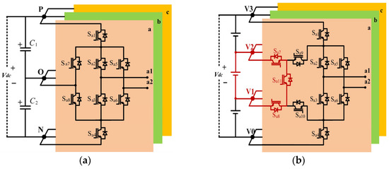
Figure 1.
Topology structure of inverter: (a) topology of dual-output, active, neutral-point-clamped, three-level inverter; (b) topology of dual-output, hybrid-clamped, quasi-five-level inverter.
The three bridge arms of the proposed inverter topology share an identical structure, with each phase comprising 11 switches, denoted as Sx1–Sx11 (where x represents the phase index from the set {a, b, c}). Taking phase a as an example, the external switches Sa1 and Sa4 are responsible for introducing the two outermost DC voltage levels to the internal output branches. Switches Sa2 and Sa3 constitute the first output branch, leading to the first output port a1; meanwhile, switches Sa5 and Sa6 form the second output branch, which is arranged in parallel with the first, leading to the second output port a2. Regarding the clamping mechanism, the upper clamping switches Sa7 and Sa9 introduce the 0.75 Vdc level, while the lower clamping switches Sa8 and Sa10 introduce the 0.25 Vdc level. Crucially, switch Sa11 acts as a selective link for the intermediate levels. By coordinating the conduction states of the output bridges (Sa2/Sa3 and Sa5/Sa6), it allows the two output ports to independently select and generate the desired voltage levels.
In contrast to conventional five-level inverters, the proposed topology significantly reduces the switch count while offering dual-output capability, allowing the upper and lower ports to operate independently.
2.2. Working Principle
Taking phase a as an example, the four phase voltage levels available at the circuit’s output terminals are denoted as V3, V2, V1, and V0.
When one output terminal delivers the V3 level, the conduction of switches Sa7, Sa10, and Sa11 enables the V2 level to be output to another terminal via the lower bridge arm. When one output terminal produces V0, switches Sa8, Sa9, and Sa11 conduct, allowing the V1 voltage level to be output to another terminal via the upper bridge arm. From these switch states, it can be observed that this topology provides non-unique output paths for the intermediate voltage level, thereby enabling the independent control of each set of output terminals, enhancing the modulation index, and increasing control flexibility. All valid switch states are illustrated in Figure 2. Due to effective switch multiplexing, the switch states of the upper and lower ports are completely symmetrical. Therefore, eight independent switch states are detailed, and all valid switch states are presented in Table 1.
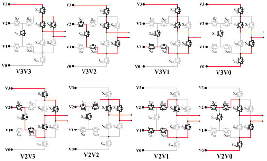
Figure 2.
Effective working states of DO-HC-FLI.

Table 1.
Effective operational status of the topological structure.
While the switching logic defines the available output paths, the specific voltage values assigned to these levels depend on the DC–link configuration. The operation of a multilevel inverter does not solely rely on a specific DC-side voltage distribution ratio. In principle, as long as the DC-side provides unequal voltage levels, a multilevel step wave can be synthesized through various switch combinations. In this context, the set of phase voltage levels (0, 0.25 Vdc, 0.75 Vdc, Vdc) adopted in this work represents an optimal solution derived from specific optimization criteria, rather than a unique feasible solution for system operation.
The gap between the chosen phase levels (0.75 Vdc–0.25 Vdc) is exactly 0.5 Vdc. This differential property allows the system to synthesize the “missing” intermediate level 0.5 Vdc in the line voltage output naturally. By selecting this specific asymmetric ratio, the resulting line-to-line voltage levels (VAB = VA − VB) are expanded to 0, 0.25 Vdc, 0.5 Vdc, 0.75 Vdc, and Vdc. This distribution ensures that the voltage steps are densely distributed in regions of rapid sinusoidal change (e.g., zero-crossing points), thereby maximizing the sampling resolution where it matters most. Consequently, this approach generates a refined nine-level staircase waveform with significantly lower harmonic content, achieving an output performance comparable to that of a standard five-level inverter.
It is worth noting that, while the output voltage levels are logically asymmetric, the underlying DC–link structure remains physically symmetric. Specifically, level V3 is generated by superimposing the voltage of VC1 onto the base potential E2. Numerically, the physical voltages across the two capacitors VC1 and VC2 are identical. Consequently, the negative impact on voltage balancing typically associated with asymmetric structures—where a high-voltage capacitor undergoes more frequent charge/discharge cycles than a low-voltage one—does not exist in this topology. The virtual vector VS1, constructed via time-averaging, ensures that the switching sequence adheres to the single-step switching principle, maintaining state continuity during critical sector transitions. By refining the granularity of the voltage synthesis in these irregular sub-sectors, the virtual vector minimizes the deviation between the reference and applied vectors, thereby reducing current ripple and improving THD performance.
To stabilize the DC–link voltage of the preceding stage, this paper employs the DC-side power supply section depicted in Figure 3, which comprises two DC power sources and two Buck chopper circuits. The first Buck converter, Buck-1, consists of switch T1, inductor L1, diode D1, and capacitor C1, and is configured as a reverse-mode Buck converter. The second Buck converter comprises switch T2, inductor L2, diode D2, and capacitor C2, and operates as a forward-mode Buck chopper circuit. The operation of two Buck converters enables the front-end DC–link to supply four distinct DC voltage levels (V3, V2, V1, V0) to the subsequent three-phase inverter circuit.
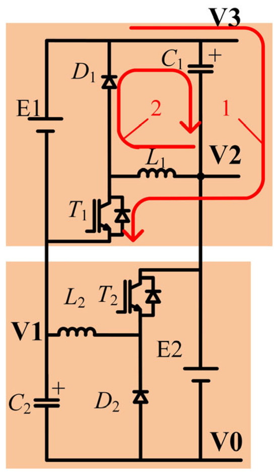
Figure 3.
Working principle of Buck-1.
The operating principle is illustrated using the first Buck converter, Buck-1, as an example, as shown in Figure 3. When the DC-side voltage V3 falls below the required voltage, since V3 is equal to the voltage of the DC power supply, E2, plus the voltage across capacitor C1 (i.e., V3 = E2 + VC1), to increase the value of V3, it is necessary to increase the voltage across capacitor C1, VC1. Consequently, the first Buck converter, Buck-1, operates. The operation of the Buck-1 converter is as follows: When switch T1 is closed, inductor L1 stores energy. The current path is from the positive terminal of DC source E1, through capacitor C1, inductor L1, and switch T1, to the negative terminal of DC source E1, as illustrated by loop 1 in Figure 3. Conversely, when switch T1 is open, due to the inability of the voltage across inductor L1 to change instantaneously, inductor L1 discharges, thereby charging capacitor C1. In this state, the current flows from inductor L1, through diode D1, to capacitor C1, as illustrated by loop 2 in Figure 3.
When the DC-side voltage V1 falls below the required level, since V1 is equivalent to the voltage across capacitor C2 (i.e., V1 = VC2) and simultaneously serves as the output voltage of the second Buck converter, Buck-2, an increase in V1 necessitates raising the voltage across capacitor C2 (VC2). The second Buck converter, Buck-2, then activates. Its operational principle mirrors that of the first Buck converter and will not be reiterated. The DC-side power provision stage of the preceding section is capable of supplying four stable DC voltage levels to the subsequent three-phase inverter topology.
2.3. Voltage and Current Stresses on the Power Switch
By analyzing the effective switching states, the blocking voltage stress across each non-conducting switch is derived.
The voltage stress distribution for the non-conducting switches in phase a is detailed as follows:
Outer switches (Sa1, Sa4): The stress varies among 0.25 Vdc, 0.375 Vdc, 0.5 Vdc, and 0.75 Vdc. Notably, 56% of the operating states correspond to the lowest stress level of 0.25 Vdc.
Hybrid clamping switches (Sa7, Sa8): These switches withstand discrete levels of 0, 0.25 Vdc, and 0.5 Vdc, with 67% of the states clamping at 0.5 Vdc.
Central switch (Sa11): This component is subjected to a fixed peak stress limit of 0.5 Vdc.
Clamping switches (Sa9, Sa10): The stress levels include 0.25 Vdc, 0.375 Vdc, 0.5 Vdc, and 0.75 Vdc, with 44% of instances at 0.25 Vdc.
Inner switches (Sa2, Sa3, Sa5, and Sa6): These switches experience the broadest range of stress, covering 0.25 Vdc, 0.375 Vdc, 0.5 Vdc, 0.75 Vdc, and Vdc.
To obtain a comprehensive assessment of the switch’s actual operating conditions, it is necessary to look beyond peak voltage and consider both the magnitude of the voltage stress and the duration of each operating state. Therefore, this paper adopts the time-average voltage stress (TAVS) as a key metric. A lower time-average voltage stress signifies that the switch experiences reduced voltage across the majority of its switching states, which in turn can mitigate switching losses (particularly turn-off losses). The hybrid clamping switches ensure that the switching states of this topology are complete and symmetrically distributed, making it highly suitable for calculating the time-average voltage stress. This metric quantifies the time-weighted operating voltage of the switch, thus enabling a more accurate assessment of the overall voltage stress level.
Calculations reveal that the time-averaged voltage stress on Sa1 and Sa4 is 0.403 Vdc, on Sa2, Sa3, Sa5, and Sa6 is 0.547 Vdc, on Sa7 and Sa8 is 0.4375 Vdc, and on Sa9 and Sa10 is 0.484 Vdc. Sa11 remains in the ON state for most of the time, experiencing 0.5 Vdc for only a very short duration.
In three-level NPC inverters, switching devices typically withstand voltage stress of 0.5 Vdc or higher. For five-level, diode-clamped inverters, the peak voltage across switching devices often reaches 0.5 Vdc or more, with the average voltage stress potentially approaching 0.5–0.6 Vdc. Therefore, the TAVS across all switching devices in the proposed topology is significantly lower than the typical levels found in conventional five-level topologies. This reduced voltage stress allows for the consideration of power devices with slightly lower voltage ratings or superior on-resistance, while still satisfying safety margins, which helps to reduce system costs and decrease heat sink size.
The current flowing through the switching devices is a critical factor in determining inverter losses, junction temperature, and efficiency, which in turn dictates the overall performance of the power electronic equipment. Therefore, it is necessary to investigate the current carried by the switching devices within the topology.
Due to the inherent symmetry of the topological structure, the analysis of current paths is confined to the switching devices in the upper half. For a detailed illustration, the switching devices of the phase a bridge arm are selected. Let the current flowing out from the upper output terminal be i1 and the current flowing out from the lower output terminal be i2, with the outward direction defined as positive. By formulating Kirchhoff’s Current Law (KCL) equations within the circuit, the currents flowing through each switching device can be derived, as presented in Table 2.
Table 2.
Instantaneous current of the switch tube corresponding to different switch states.
2.4. Comparative Analysis and Scalability Discussion
The proposed topology is benchmarked against existing dual-output converters in Table 3, focusing on component count, voltage levels, and modulation flexibility.
Table 3.
Comparison between the previous topologies and the proposed topology.
It can be observed that, similar to the conventional independent NPC five-level inverter, the proposed structure supports unrestricted dual outputs and generates 9-level line voltages. However, by leveraging switch multiplexing, it achieves this with a reduced number of switches. Furthermore, compared to other switch-sharing counterparts, this topology successfully realizes mutually independent modulation ranges for both output ports while ensuring high output quality.
3. Modulation Strategy and Loss Analysis
Following the analysis of the topology and operating principles of the DO-HC-FLC presented in the previous chapter, this chapter focuses on its core modulation strategy and system losses. In existing research, time-sharing modulation has been commonly employed in dual-output topologies; however, it presents significant challenges in multi-port multilevel inverters, including limited degrees of freedom, degraded waveform quality, and uneven thermal distribution. Leveraging the unique hybrid clamping mechanism of the quasi-five-level topology, this chapter proposes a fully decoupled dual-output SVPWM strategy. This strategy achieves independent control of the dual-output ports in terms of frequency, amplitude, and modulation index by reconfiguring the clamping paths.
Furthermore, to comprehensively evaluate the efficiency performance of the proposed system, a detailed analysis of power loss characteristics is presented. Based on the calculated loss distribution, the overall system efficiency is further investigated across a wide range of modulation indices.
3.1. Analysis of Modulation Strategy
Given the asymmetric DC source configuration and the dual-output characteristics of this topology, traditional standard SVPWM algorithms are not directly applicable. Consequently, this chapter establishes a hierarchical modulation framework, the overall control block diagram of which is illustrated in Figure 4. The core concept of this strategy is to decompose the complex dual-output modulation task into two independent single-output modulation processes, which are then synthesized through a subsequent logic decision stage. As shown in the figure, the control flow consists of three main phases:
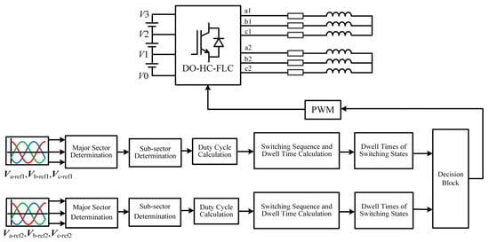
Figure 4.
Implementation flowchart of dual-output SVPWM.
Major Sector Determination is first performed for the two sets of reference voltages (Vref1 and Vref2). This is followed by precise Sub-sector Determination within the asymmetric vector space to address the mapping challenges caused by the non-uniform voltage-level distribution. Upon determining the sub-sector, the Duty Cycle Calculation is executed. Subsequently, the Switching Sequence and Dwell Time Calculations are performed. Adhering to the principle of minimum switching transitions, the algorithm arranges the switching states and determines their dwell times for each basic voltage vector to ensure efficient operation. The switching states generated from both parallel channels are ultimately input into the Decision Block. This module is responsible for managing the coupling relationship between the two channels and synthesizing the final PWM driving signals, ensuring that the inverter can drive both loads (Load 1 and Load 2) simultaneously and independently. The subsequent sections will provide a detailed analysis of the implementation principles and logic design for the Major Sector Determination, Sub-sector Determination algorithms, Dwell Time Calculations under asymmetric conditions, and the Decision Block, respectively.
Assume that the three-phase reference voltage for the n-th output group is:
In the equation, Vm, ωn, and φn denote the amplitude, angular frequency, and initial phase of the three-phase reference voltage, respectively. Thus, the reference voltage vector Vrefn for the n-th output group is given by:
Let V1, V2, and V3 be the three fundamental vectors involved in synthesizing the reference vector Vr. Their respective active durations are T1, T2, and T3, and the sampling period is Ts. Substituting these into the volt–second balance equation yields:
The space vector diagram for the first major sector under the SVPWM modulation scheme is illustrated in Figure 5a. Considering the reference vector Vrefn located within the fourth sub-sector of the first major sector, as illustrated in Figure 5b.
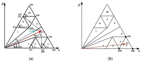
Figure 5.
Sub-sector distribution and synthesis principle: (a) sub-sector division of Sector I; (b) vector synthesis in the fourth sub-sector of Sector I.
Referring to the position of Vref in Figure 5a, the partition of minor sectors is determined by the angles formed by connecting Vref to specific points. Consequently, the identification logic relies on the angular orientation of the lines linking Vref to these key nodes. The mathematical definitions of these parameters are as follows:
The angle between the reference voltage vector Vr and the α-axis is θ, the angle with vector V210 is R1, and the angle with vector V321 is R2. Vr connects to (2(V2 − V1)/3, 0) with an angle of γ1 to the α-axis; to (2 V2/3, 0) with an angle of γ2 to the α-axis; to (V2/3, √3 V2/3) with an angle of γ3 to the π/3 direction; and to ((V2 − V1)/3, √3(V2 − V1)/3) with an angle of γ4 to the π/3 direction.
Initially, based on the angles of R1 and R2, the reference vector is located within one of the constituent sub-sectors (labeled 1, 5, 6, or 7) that comprise the 60° sector. R1 and R2 are calculated as follows:
The specific sub-sector among 2, 3, and 4 is identified using the angles γ1 and γ2, whereas the location among sub-sectors 8, 9, and 10 is derived from γ3 and γ4. γ1, γ2, γ3, and γ4 are calculated as follows:
After identifying the sector of Vrefn, the vectors V200, V300, and V310 are selected for synthesis based on the nearest three-vector principle. Applying the volt–second balance principle allows for the calculation of the dwell times and duty cycles of each basic vector, thereby determining the specific switching sequence. The calculation equations are as follows:
The corresponding action times T1, T2, and T3 for the three fundamental vectors are obtained. The three fundamental vectors contributing to the synthesis in region I4 are V200, V300, and V310, with their respective action times being:
The switching sequence of SVPWM is not unique. To prevent voltage transient issues, the switching sequence adopted in this paper is presented in Table 4 (switching sequence for the A1 major sector). Once the switching sequence and the active times of the synthesized vectors are determined, the active times for each switch can be obtained. By combining the vector active times with the vector states, a symmetrical five-segment SVPWM waveform can be derived, as shown in Figure 6.
Table 4.
Vector order of the first sub-sector in Sector I.
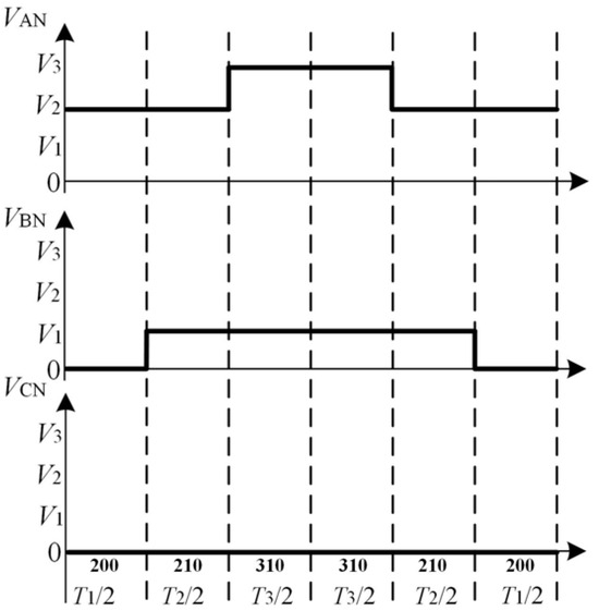
Figure 6.
The switching time of the inverter.
The final pulse-width modulation pulses are then derived based on the active time of each switch during its respective switching state. As depicted in the figure, Sectors I, III, and V share an identical calculation method, while Sectors II, IV, and VI are calculated identically (and symmetrically to Sector I). This characteristic effectively reduces the complexity of the space vector pulse width modulation algorithm.
Figure 7a and Figure 7b respectively present the space vector distribution diagrams for the first major sector of the quasi-five-level inverter and the conventional five-level inverter. Due to the differing DC–link voltage values of the quasi-five-level inverter, this characteristic offers a significant advantage for its sector division scheme: its first major sector only requires partitioning into a smaller number of sub-sectors with simpler structures.
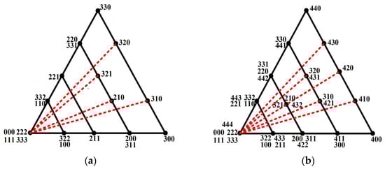
Figure 7.
Space voltage vector distribution diagram: (a) vector distribution in the first major sector of the quasi-five-level inverter; (b) vector distribution in the first major sector of the five-level inverter.
The space vector distribution for each major sector of the quasi-five-level inverter is shown in Figure 8. Each three-phase voltage level state of the two output groups corresponds to a space vector. The space vector diagram for each output group is divided into six major sectors, defined as An to Fn, respectively, where n ∈ {1, 2} represents the first and second output groups. Following the simplification of active vectors, each major sector can be divided into 10 sub-sectors.
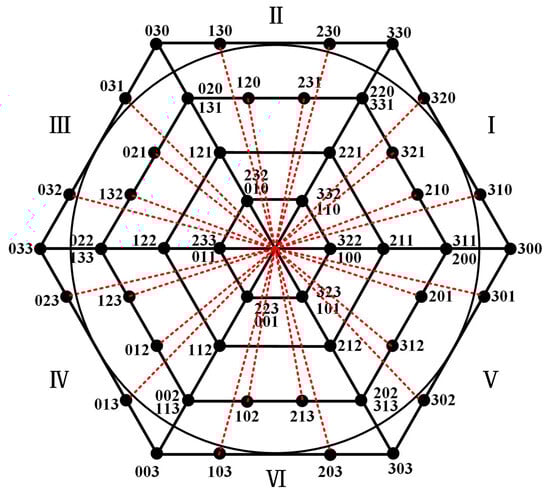
Figure 8.
Quasi-five-level voltage space vector distribution diagram.
To address the discontinuities inherent in the unique level structure, virtual vectors are introduced in the fifth and sixth sub-sectors to optimize the switching transient performance during sector transitions. By constructing the virtual vector VS1 = 5(V221 + V211)/6, spatial vector modulation is performed using differentiated basic vector combinations based on the specific positions within the fifth and sixth sub-sectors. Specifically, within the lower half of the fifth sub-sector, the vector required for voltage synthesis is V210, VS1(V211, V221), V222. In the upper half of the same sector, synthesis is performed using vectors V210, V310, and V320. This modulation strategy ensures that all voltage vectors can be effectively and continuously synthesized throughout the entire vector space, particularly in critical sector transition region. This achieves seamless coverage and smooth switching across all sub-sectors.
From an implementation perspective, the active synthesis of virtual vectors using existing switching states, rather than increasing the system burden, effectively reduces both control complexity and sensor requirements. This is because the method relies entirely on a software-based time-averaging algorithm that achieves precise waveform construction without the need for any additional hardware balancing circuits or an increased number of sensing components. Simultaneously, this synthesis logic is based on deterministic algebraic operations, avoiding the complex redundant state optimization or computations common in conventional methods, thereby significantly simplifying the implementation of the control system. The deployment of the virtual vector fundamentally optimizes the commutation trajectory. By inserting this intermediate state, the modulation enforces a strict nearest-level transition principle. This effectively mitigates long-distance vector jumps (e.g., sudden transitions across 0.5 Vdc) and constrains the voltage step magnitude of each commutation to the minimum unit (0.25 Vdc). Such a mechanism not only prevents uncontrolled transients caused by simultaneous multi-device transitions but also significantly reduces the voltage stress (dv/dt) across the switches during commutation. Consequently, this leads to a direct reduction in the cumulative switching energy dissipation (Eon/Eoff) and an improvement in electromagnetic interference (EMI) performance.
The vector distributions of other major sectors are similar to that of A1. Given the four output voltage level states: V3, V2, V1, and V0, and after simplification, there are 52 fundamental output voltage space vectors, as detailed in Table 5.
Table 5.
Output voltage space vector of dual-output hybrid-clamped quasi-five-level inverter. (X = 2V3/3, Y = 2V2/3, Z = X − Y = 2V1/3, W = Y − Z, k = ejπ/3).
3.2. Inverter Loss Analysis
During operation, power device losses are primarily categorized into three types: conduction loss, off-state loss, and switching loss. Specifically, due to the small leakage current of the switching device in its off-state, off-state losses are typically considered negligible in engineering calculations. This paper proceeds to analyze the calculation methods for the conduction loss and switching loss of the switching device.
Given that the initial saturation voltage drop and on-resistance of the switching device vary approximately linearly with temperature, the initial saturation voltage drop v0,T and on-resistance rT of the switching device are expressed as:
where v0,T_25 °C and rT_25 °C are the initial saturated voltage drop and on resistance of the switch at junction temperature of 25 °C, respectively; Kv0,T and Kr,T are the temperature correction coefficients of the initial saturation voltage drop and on resistance, respectively; Tj,T is the junction temperature of the switch tube. Therefore, the conduction loss Pcond,T of the switch tube is calculated as
where IT is the instantaneous current value flowing through the switch tube.
The switching loss of the switch tube is composed of on loss and off loss, and the calculation formula is
where Asw,T, Bsw,T, Csw,T are the quadratic fitting curve coefficients of the switching loss of the switch tube with respect to the current; Uce is the actual withstand voltage of the switch tube; Ubase is the test voltage; T is the actual temperature of the switch tube; Tbase is the test temperature; Dsw,T, ksw,T are the voltage correction factor and temperature correction factor of switching loss of switch tube, respectively.
In a switching cycle, the average switching loss of the switch is
where fsw is the switching frequency. The loss of anti-parallel diode in the process of turning on is very small and can be ignored.
The thermal model of DO-HC-FLI was established when f1 = 50 Hz, f2 = 100 Hz, m1 = 0.95, m2 = 0.95, fs = 10 kHz, Vdc = 48 V, R1,2 = 10 Ω, L1,2 = 10 mH. Figure 9 shows the total loss distribution of each switching device of phase a under four commutation modes.
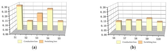
Figure 9.
Switch loss distribution: (a) S1–S5 loss distribution; (b) S6–S10 loss distribution.
4. Simulation Results and Analysis
4.1. Output Waveform Analysis
To verify the feasibility of the dual-output, hybrid-clamped, quasi-five-level inverter, a simulation model will be established in the Matlab (R2021a)/Simulink environment. The simulation parameters are as follows: the DC power supply voltage is 450 V, the capacitance of capacitors C1 and C2 is 75F, and the resistive–inductive (RL) load is configured with R = 10 Ω and L = 10 mH. By adjusting the two Buck step-down circuits at the front end, the four output levels can be controlled as follows: V3 = 600 V, V2 = 450 V, V1 = 150 V, V0 = 0.
The proposed inverter is tested in both same-frequency and different-frequency modes. Furthermore, to verify the independence of the two AC output ports under load variations, two identical sets of three-phase loads are connected in parallel to one port. At t = 0.1 s, one set of loads is disconnected, and the three-phase output currents of the other port are observed to check for any cross-interference.
The experimental line voltage waveforms Vab1 and Vab2 for Mode a operation are depicted in Figure 10a,b. Both output sets exhibit a clear nine-level staircase structure, with voltage levels at ±600 V, ±450 V, ±300 V, ±150 V, and 0 V. The measured fundamental amplitude for both groups is 599 V, which closely matches the theoretical value of 597.6 V. Further spectral analysis is presented in the FFT results shown in Figure 10c,d. The measured total harmonic distortion (THD) is 20.37%. Crucially, the spectral distribution demonstrates that low-order harmonics (e.g., 5th and 7th orders) are effectively suppressed, verifying the efficacy of the proposed modulation strategy. Instead, the harmonic energy is predominantly concentrated in high-frequency bands near the switching frequency. This characteristic is highly advantageous for practical applications, as these high-frequency components are easily attenuated by the inductive nature of the load.
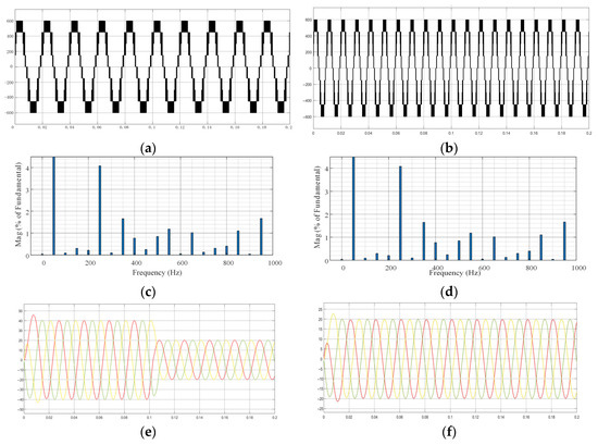
Figure 10.
Simulation waveforms with f1 = f2 = 50 Hz and m1 = m2 = 1.15: (a) line voltage Vab1; (b) line voltage Vab2; (c) harmonic spectrum of Vab1; (d) harmonic spectrum of Vab2; (e) three-phase current iabc1; (f) three-phase current iabc2.
When these voltages are applied to the load, balanced three-phase sinusoidal currents are obtained, as illustrated in Figure 10e,f. To evaluate the dynamic performance, a sudden load change test was conducted. It can be observed that the output current amplitude responds instantly to the step change. The current decreases immediately to approximately half of its initial value with a smooth transition, exhibiting no noticeable overshoot or oscillation, while the other port remains unaffected. This stable and rapid transient behavior validates the excellent dynamic response capability of the controller.
The simulation waveforms of the two output line voltages, Vab1 and Vab2, are shown in Figure 11a,b for mode a operation. As the modulation index decreases, the line voltage in Figure 10b changes to seven levels. In each basic cycle, the duration of the ±600 V levels decreases, while the duration of the ±450 V, ±300 V, and ±150 V levels increases. Figure 11c,d display the FFT analysis results for the two output line voltages.
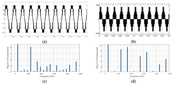
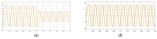
Figure 11.
Simulation waveforms with f f1 = f2 = 50 Hz, m1 = 1.15, m2 = 0.566: (a) line voltage Vab1; (b) line voltage Vab2; (c) harmonic spectrum of Vab1; (d) harmonic spectrum of Vab2; (e) three-phase current iabc1; (f) three-phase current iabc2.
In mode c, the two sets of outputs are in different frequency modes. Figure 12a,b present the measured waveforms of the two output line voltages, Vab1 and Vab2. It can be seen that the output line voltages of both groups can still maintain nine levels and can operate at maximum modulation. The FFT results for line voltages Vab1 and Vab2 are shown in Figure 12c,d. It can be seen that the fundamental wave amplitudes of the two sets of output line voltages are 601.2 V and 599.2 V, respectively, while the theoretical value is 597.6 V. The output voltage amplitudes closely match the theoretical values. Most harmonic components in Vab1 and Vab2 appear around the switching frequency and its integer multiples. Figure 12e,f confirm that the load currents remain highly sinusoidal throughout the dynamic process.
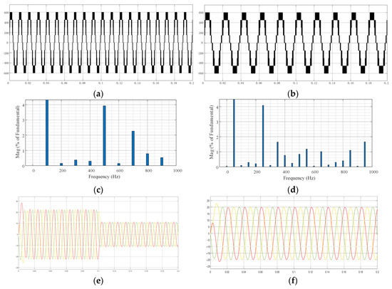
Figure 12.
Simulation waveforms with f1 = 100 Hz, f2 = 50 Hz, m1 = m2 = 1.15: (a) line voltage Vab1; (b) line voltage Vab2; (c) harmonic spectrum of Vab1; (d) harmonic spectrum of Vab2; (e) three-phase current iabc1; (f) three-phase current iabc2.
In mode d, the simulation waveforms of the output line voltages Vab1 and Vab2 are shown in Figure 13a,b. Figure 13c,d analyze the FFT of two sets of output line voltages. The experimental waveforms show that the first set of outputs has seven levels, and as the modulation index decreases, the fundamental amplitude decreases, while the second set of outputs still has nine levels. As shown in Figure 13e,f, the dynamic response to the load step remains effective even at an output frequency of 100 Hz, while maintaining a symmetrical sinusoidal waveform.
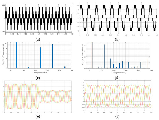
Figure 13.
Simulation waveforms with f1 = 100 Hz, f2 = 50 Hz, m1 = 0.566, m2 = 1.15: (a) line voltage Vab1; (b) line voltage Vab2; (c) harmonic spectrum of Vab1; (d) harmonic spectrum of Vab2; (e) three-phase current iabc1; (f) three-phase current iabc2.
4.2. Harmonic Performance and Efficiency Analysis
Total harmonic distortion (THD) is quantified as the root mean square (RMS) magnitude of the harmonic components divided by the RMS magnitude of the fundamental component in the inverter’s output waveform.
where V1 is the RMS value of the fundamental component, and Vn is the RMS value of the nth harmonic component (n = 1, 2, …).
To simultaneously account for the effects of both low-order harmonics and harmonics near the switching frequency, the maximum frequency for THD calculation is set to the Nyquist frequency (2500 kHz), with an output frequency of 50 Hz. Since changes in one set of outputs do not affect the THD value of the other set, the modulation index of the other set is fixed at 0.8 during THD measurement. The relationship between the two sets of output currents and the output line voltage THD values as a function of modulation indices m1 and m2 (m1, m2 ∊ [0, 1]) is shown in Figure 14. The figure reveals that, as modulation increases, the THD of the output line voltage gradually decreases. When modulation exceeds 0.5, the THD stabilizes around 25%, significantly lower than that of the ANPC.
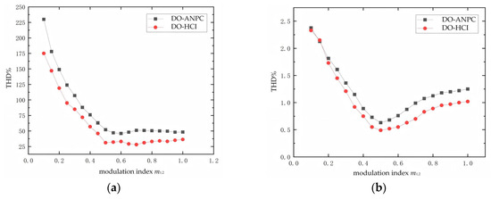
Figure 14.
Comparison of THD test results: (a) total harmonic distortion of the output current; (b) total harmonic distortion of the output line voltage.
While this value is slightly higher than that of fully populated five-level inverters, it represents a highly favorable trade-off for space-constrained and cost-sensitive applications. Unlike conventional topologies that require massive hardware redundancy to achieve minimal THD, the proposed structure utilizes a minimal component count to realize dual-port independent control and nine-level voltage synthesis. This unique feature makes it exceptionally suitable for compact dual-drive systems (e.g., dual-motor electric vehicles or conveyor belts), where reducing system volume and weight is prioritized over achieving marginally lower voltage THD. Furthermore, the spectral distribution confirms the design’s practicality: the harmonics are primarily concentrated at high frequencies. When applied to inductive loads, these high-order harmonics are naturally filtered, resulting in a high-quality sinusoidal current. Thus, the topology successfully bridges the gap between the simplicity of three-level inverters and the performance of multilevel inverters, offering an optimal solution for scenarios demanding high power density.
To further evaluate the power conversion capability of the proposed topology, the system efficiency under different modulation indices is investigated. Figure 15 illustrates the efficiency curve where both ports operate symmetrically with the same modulation index. As observed, the efficiency exhibits a positive correlation with the modulation index. In the low-modulation region (m < 0.4), the efficiency is relatively low. This is primarily because the effective output voltage and power are small, while the constant losses account for a significant proportion of the total energy. In the high modulation region (m > 0.8), the efficiency improves significantly and stabilizes. Since the output power increases quadratically with the voltage, the growth in effective output power dominates over the increase in conduction and switching losses. Consequently, the inverter achieves its optimal performance in the linear modulation range near unity, reaching a peak efficiency of 97.2% at the rated output power of 32.6 kW.
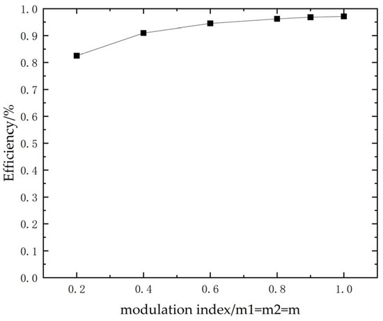
Figure 15.
Simulated efficiency and total output power versus modulation index under symmetrical operation (m1 = m2).
5. Experimental Results
To validate the effectiveness of the proposed topology and modulation scheme, an experimental prototype of the DO-HC-FLI was built, as shown in Figure 16. The prototype includes a controller board, driver circuits, a main circuit, and two sets of three-phase loads. The control functions are jointly implemented by an FPGA-based PWM driving signal generation unit. The FPGA used is an Altera Cyclone IV series EP4CE115F23I7N, and the power devices are model IPW60R060P7.
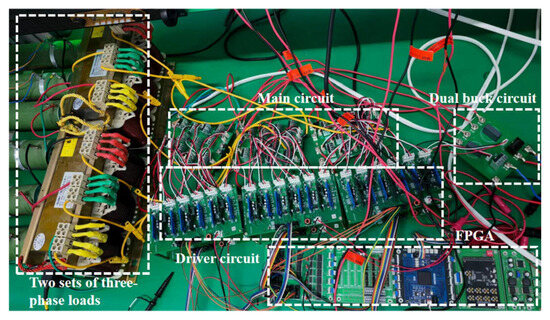
Figure 16.
Experimental platform.
In order to validate the independent control capability and the high DC voltage utilization of the proposed topology, the experimental verification was performed under asymmetrical conditions (i.e., distinct frequencies and amplitudes). This setup presents a more rigorous test than the symmetrical scenario, thereby confirming that the two outputs function independently without mutual coupling. The parameters of the experimental platform are shown in Table 6.
Table 6.
System parameters and testing parameters.
To verify the uniqueness of the topology, experimental parameters were set with different modulation indices for the upper and lower output ports and at different frequencies. Figure 17 shows the three DC voltage levels V3, V2, and V1 output by the Buck converters. Figure 18a,b show, respectively, the line voltage waveforms between phases a1 and b1, and between phases a2 and b2, at reference voltage frequencies of 50 Hz and 100 Hz.
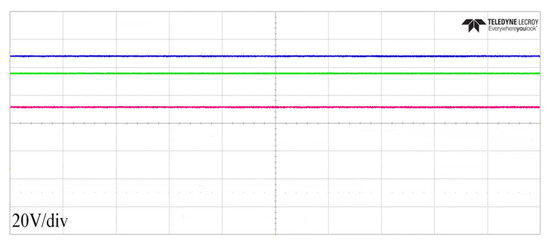
Figure 17.
Four DC levels output by the front end.
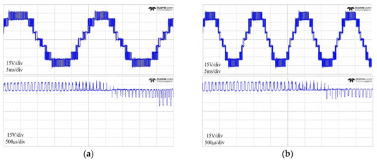
Figure 18.
Line voltage waveforms: (a) upper output port; (b) lower output port.
As illustrated in Figure 18a,b, the proposed inverter generates a clear nine-level staircase line voltage waveform. The distinct voltage levels demonstrate the correct synthesis of the voltage vectors. Crucially, despite the distinct modulation indices and frequencies applied to the upper and lower ports, the voltage waveforms remain stable and undistorted. This experimental result strongly corroborates the decoupling capability of the proposed topology, verifying that the operation of one port does not impose interference on the other, even under asymmetrical conditions.
Furthermore, it can be observed from Figure 19a,b that, after simple filtering of the DO-HC-FLI output, good sinusoidal output voltage and current can be obtained. This is attributed to the multilevel characteristic of the DO-HC-FLI, which significantly reduces the voltage stress (dv/dt) and the harmonic content compared to traditional inverters. The smooth current waveforms further indicate the high tracking accuracy of the control strategy and the low current distortion.
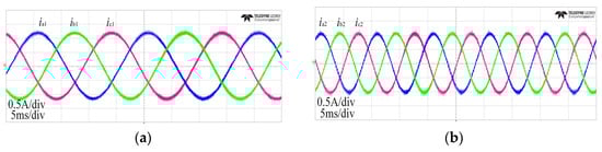
Figure 19.
Three-phase output current waveforms: (a) upper output; (b) lower output.
Figure 20a,b present the FFT analysis of the line voltages Vab1 and Vab2. It is evident that the low-order harmonics are effectively suppressed, and the harmonic energy is primarily distributed around the switching frequency and its multiples. This high-frequency distribution implies that the harmonics can be easily filtered out by small-sized passive components. Consequently, the measured total harmonic distortion (THD) is maintained at a low level, which satisfies the standard requirements and verifies the effectiveness of the proposed modulation scheme.
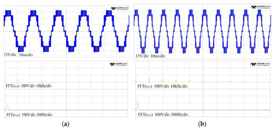
Figure 20.
Experimental FFT spectrum of line voltage: (a) upper output Vab1; (b) lower output Vab2.
6. Conclusions
In this paper, a novel dual-output hybrid-clamped quasi-five-level inverter topology is proposed to address the limitations of existing dual-output architectures, specifically the constraints on modulation indices and low DC–link voltage utilization. By integrating a hybrid clamping mechanism with an optimized control strategy, the proposed topology successfully combines the advantages of multi-port integration and high-quality multilevel waveform output. The specific conclusions are drawn as follows:
- (1)
- Innovative topology structure and flexibility: The topology of the proposed inverter allows for adjacent voltage level outputs at the dual ports. This design not only realizes a quasi-five-level output with reduced component redundancy but also eliminates the rigid sequential constraints found in traditional vertically stacked topologies. The structural flexibility allows for the selection of optimal switching paths within a single cycle, establishing a solid foundation for high-performance power conversion.
- (2)
- Decoupled control and enhanced voltage utilization: A coordinated modulation strategy is developed to effectively decouple the control of the two output ports. Unlike traditional time-sharing schemes where the operation of one port restricts the other, the proposed method ensures that the modulation index ranges of both outputs remain unconstrained and mutually non-interfering. This breakthrough significantly improves DC–link voltage utilization, allowing the system to adapt to complex asymmetric loading conditions and diverse frequency requirements without performance degradation.
- (3)
- Superior waveform quality via line voltage synthesis: Through the strategic alignment of phase voltage levels and their differential superposition, the proposed topology achieves a nine-level line voltage output. This optimized synthesis method enables the inverter to track sinusoidal reference trajectories with high precision using a simplified phase structure. Consequently, the output waveform exhibits a high degree of sinusoidal approximation with significantly reduced total harmonic distortion (THD), making it highly suitable for grid-connected renewable energy systems and sensitive motor drive applications.
Future work will investigate active balancing circuits or advanced redundant-state selection algorithms to address this stability issue. In parallel with voltage control, although the current spectral performance is satisfactory, implementing advanced control strategies, such as Model Predictive Control (MPC), could further optimize THD and dynamic response beyond the capabilities of the current SVPWM scheme. From a reliability perspective, given the reduced component count, the impact of a single switch failure on the dual-output functionality warrants detailed investigation. By leveraging structural integration and control decoupling, the proposed topology achieves exceptional power density in dual-motor electric vehicle (EV) powertrains and cost-effective multi-functional integration in microgrid applications. Furthermore, through a modular cascaded configuration, it possesses the scalability to smoothly transition toward medium-voltage and high-power scenarios. Ultimately, these targeted advancements will bridge the gap between theoretical innovation and industrial deployment, establishing the proposed topology as a competitive solution for next-generation power conversion systems.
Author Contributions
Conceptualization, R.W.; Methodology, R.W.; Software, J.W.; Validation, J.W.; Resources, R.W.; Writing—original draft, J.W.; Visualization, Y.Y.; Supervision, Y.Y.; Funding acquisition, Y.Y. All authors have read and agreed to the published version of the manuscript.
Funding
This research received no external funding.
Data Availability Statement
The original contributions presented in this study are included in the article. Further inquiries can be directed to the corresponding author.
Conflicts of Interest
The authors declare no conflict of interest.
Abbreviations
| DO-HC-FLI | dual-output, hybrid-clamped, quasi-five-level inverter |
| NPC | neutral-point-clamped |
| ANPC | active neutral-point-clamped |
| SVPWM | space vector pulse width modulation |
| VSVPWM | virtual space vector pulse width modulation |
| PV | photovoltaic |
| EMI | electromagnetic interference |
| HB | H-bridge |
| FC | flying capacitor |
| MVS | maximum voltage stress |
| TAVS | time-average voltage stress |
| THD | total harmonic distortion |
| RMS | root mean square |
| SC | switched capacitor |
| RL | resistive–inductive |
| MPC | Model Predictive Control |
| EV | electric vehicle |
References
- Wang, Y.; Li, N.; Zhao, Z.; Liang, J.; Zeng, G. A new type of multilevel inverter and its modular analysis. Trans. China Electrotech. Soc. 2022, 37, 4676–4687. [Google Scholar] [CrossRef]
- Yang, X.; Chang, J.; Wang, X. T-type inverter feed-through open-winding permanent magnet synchronous motor SVM strategy. Power Electron. 2022, 56, 57–60. [Google Scholar]
- Dyanamina, G.; Kakodia, S.K. Adaptive neuro fuzzy inference system based decoupled control for neutral point clamped multilevel inverter fed induction motor drive. Chin. J. Electr. Eng. 2021, 7, 70–82. [Google Scholar]
- Srivastava, A.; Seshadrinath, J. A new nine-level highly efficient boost inverter for transformerless grid-connected PV application. IEEE J. Emerg. Sel. Top. Power Electron. 2023, 11, 2730–2741. [Google Scholar] [CrossRef]
- Zhao, T.; Chen, D. A power adaptive control strategy for further extending the operation range of single-phase cascaded H-bridge multilevel PV inverter. IEEE Trans. Ind. Electron. 2022, 69, 1509–1520. [Google Scholar] [CrossRef]
- Peddapati, S.; Prasadarao, K.V.S. A new fault-tolerant multilevel inverter structure with reduced device count and low total standing voltage. IEEE Trans. Power Electron. 2022, 37, 8333–8344. [Google Scholar] [CrossRef]
- Wang, L.; Han, X.; Li, Z.; Yang, L. A novel flying-capacitor Zeta multilevel inverter. Trans. China Electrotech. Soc. 2022, 37, 254–265. [Google Scholar] [CrossRef]
- Ye, M.; Yu, S.; Liu, W.; Chen, Y.; Shao, Y. Linear power balance strategy for asymmetric cascaded H-bridge nine-level inverter. Trans. China Electrotech. Soc. 2024, 39, 4495–4507. [Google Scholar] [CrossRef]
- Zhang, H.; Wu, Y.; Li, H.; Yin, S.; Jin, S.; Lin, S.; Jiang, T.; Cheng, Y. Design and evaluation of a 1200-V/200-A SiC three-level NPC power module. IEEE Trans. Ind. Appl. 2023, 59, 6412–6426. [Google Scholar] [CrossRef]
- Haruna, J.; Matano, Y.; Funato, H. Efficiency improvement for diode-clamped linear amplifier using unequally divided voltage power supply. IEEE Trans. Ind. Appl. 2021, 57, 2666–2672. [Google Scholar] [CrossRef]
- Guo, F.; Ma, Z.; Diao, F.; Zhao, Y.; Wheeler, P. Hybrid virtual coordinate-driven CBPWM strategy of three-level T-type NPC converters for electric aircraft propulsion applications. IEEE Trans. Ind. Electron. 2024, 71, 2309–2319. [Google Scholar] [CrossRef]
- Prasad, T.; Pattnaik, S. Simulation for fault forbearance operation for three-phase three-level H-bridge multilevel inverter by space vector modulation technique. In Proceedings of the 2020 First International Conference on Power, Control and Computing Technologies (ICPC2T), Raipur, India, 3–5 January 2020; IEEE: New York, NY, USA, 2020; pp. 385–389. [Google Scholar]
- Babaei, E.; Laali, S.; Alilu, S. Cascaded multilevel inverter with series connection of novel H-bridge basic units. IEEE Trans. Ind. Electron. 2014, 61, 6664–6671. [Google Scholar] [CrossRef]
- Ning, J.; Ben, H.; Li, J.; Wang, X.; Meng, T. A small-sized high-precision digital closed-loop modulation method for dead-time compensation for flying capacitor three-level inverters. IEEE Trans. Power Electron. 2024, 39, 3968–3973. [Google Scholar]
- Song, L.; Duan, S.; Wang, T.; Liu, X. A simplified flying capacitor voltage control strategy for hybrid clamped three-level boost converter in photovoltaic system. IEEE Trans. Ind. Electron. 2022, 69, 8004–8014. [Google Scholar]
- Gao, Z.; Wang, L.; Zhou, Z.; Geng, C.; Wu, X. Research on bipolar carrier pulse width modulation strategy for low modulation ratio regions in three-level inverters. Chin. J. Electr. Eng. 2023, 43, 7254–7268. [Google Scholar] [CrossRef]
- Qiu, X.; Hu, Q.; Qiu, C. A dual-output quasi-five-level inverter and its VSVPWM algorithm. Control Eng. China 2024, 31, 2080–2088. [Google Scholar] [CrossRef]
- Wang, R.; Ai, L.; Liu, C. A novel three-phase dual-output neutral-point-clamped three-level inverter. IEEE Trans. Power Electron. 2021, 36, 7576–7586. [Google Scholar] [CrossRef]
- Wang, Y.; Yuan, Y.; Li, G.; Ye, Y.; Wang, K.; Liang, J. A T-type switched-capacitor multilevel inverter with low voltage stress and self-balancing. IEEE Trans. Circuits Syst. I Regul. Pap. 2021, 68, 2257–2270. [Google Scholar] [CrossRef]
- Lee, S.S.; Bak, Y.; Kim, S.M.; Lee, K.B. New family of boost switched-capacitor seven-level inverters (BSC7LI). IEEE Trans. Power Electron. 2019, 34, 10471–10479. [Google Scholar] [CrossRef]
- Lee, S.S. Single-stage switched-capacitor module (S3CM) topology for cascaded multilevel inverter. IEEE Trans. Power Electron. 2018, 33, 8204–8207. [Google Scholar]
- Wang, X.; Xie, Y.; Wang, R. A three-phase dual-output active neutral clamping three-level inverter. Trans. China Electrotech. Soc. 2024, 39, 5786–5799+5854. [Google Scholar] [CrossRef]
- Rodriguez, J.; Lai, J.-S.; Fang, Z. Multilevel inverters: A survey of topologies, controls, and applications. IEEE Trans. Ind. Electron. 2002, 49, 724–738. [Google Scholar] [CrossRef]


Disclaimer/Publisher’s Note: The statements, opinions and data contained in all publications are solely those of the individual author(s) and contributor(s) and not of MDPI and/or the editor(s). MDPI and/or the editor(s) disclaim responsibility for any injury to people or property resulting from any ideas, methods, instructions or products referred to in the content. |
© 2026 by the authors. Licensee MDPI, Basel, Switzerland. This article is an open access article distributed under the terms and conditions of the Creative Commons Attribution (CC BY) license.