Abstract
This paper investigates a dual-active-bridge (DAB) converter topology based on a voltage-doubler rectifier and series resonant network. By integrating phasor-domain analysis with time-domain modeling, a comprehensive mathematical model of the output voltage and instantaneous inductor current is established. The voltage gain expression is further refined by accounting for the effects of dead-time and power switch output capacitance. Based on this model, a multi-objective global optimization is performed, aiming to minimize reactive power, RMS current, and switch conduction losses, while simultaneously satisfying zero-voltage switching (ZVS) conditions and voltage gain requirements. Leveraging the optimization results, an extended phase-shift control strategy incorporating phase-shift feedforward and frequency closed-loop regulation is proposed. Experimental results demonstrate that the proposed topology achieves high efficiency across the entire operating range, with a peak efficiency of 96.92%. The results validate the effectiveness and engineering practicability of both the topology and the control scheme.
1. Introduction
With the rapid development of photovoltaic and energy storage systems, high-efficiency and high-power-density power electronic converters have become key enablers for efficient energy conversion and flexible power management [1,2]. The series-resonant dual-active-bridge (SRDAB) converter, as an evolution of the conventional dual-active-bridge (DAB) topology [3,4], offers significant advantages such as inherent soft-switching capability, bidirectional power flow, and galvanic isolation [5]. These features make it highly promising for applications in solid-state transformers, renewable energy storage systems, bidirectional electric vehicle charging, and micro-inverters [6,7,8,9]. Compared to the traditional DAB, the SRDAB incorporates a series resonant tank, which extends the soft-switching range [10], reduces voltage stress, suppresses current harmonics, and thereby enhances both power density and overall efficiency—making it a focal point of recent research in both academia and industry.
In this paper, we focus on an SRDAB topology employing a voltage-doubler rectifier on the secondary side. This configuration reduces the number of power switches on the transformer secondary, thereby lowering conduction losses and further improving power density, which is particularly advantageous for low-to-medium power applications.
Despite extensive studies on SRDAB converters, critical challenges remain unresolved, especially for topologies with voltage-doubler rectification. First, the widely adopted fundamental harmonic approximation (FHA) method simplifies modeling but neglects higher-order harmonics, leading to significant inaccuracies when the switching frequency deviates from resonance [11,12,13,14]. Second, existing optimization strategies often target only reactive power or RMS current minimization [15,16,17], yet they fail to simultaneously consider zero-voltage switching (ZVS) constraints and conduction losses, resulting in suboptimal efficiency across wide input/output ranges. Third, practical non-ideal factors such as dead time and switch output capacitance () introduce phase delays that degrade model accuracy and control performance, but they are rarely incorporated into analytical models. Finally, some advanced control schemes involve complex analytical expressions that hinder real-time implementation on embedded platforms like microcontrollers or DSPs [18].
Therefore, there exists a clear need for a comprehensive modeling and control framework, due to: (i) lack of high-fidelity models accounting for dead time and Coss-induced phase shifts; (ii) absence of a unified optimization objective balancing ZVS, conduction loss, and reactive power under wide operating conditions; and (iii) limited practicality of existing control strategies for digital implementation. To address these gaps, this paper proposes a phasor-time domain hybrid modeling approach for the voltage-doubler-based SRDAB converter, enabling accurate analysis beyond the limitations of FHA [19]. The voltage gain model is refined by incorporating the effects of dead time and , significantly improving accuracy across the entire operating range [20]. Furthermore, a novel multi-objective optimization is performed to minimize the root-mean-square (RMS) value of the switching instantaneous current, defined as , which simultaneously reduces conduction losses, reactive power, and ensures ZVS feasibility. Based on the optimization results, an extended phase-shift (EPS) control strategy with phase-shift feedforward and frequency closed-loop regulation is developed, facilitating real-time implementation on low-cost digital controllers. Experimental validation on a 3 kW prototype demonstrates a peak efficiency of 96.92%, verifying the effectiveness and engineering practicability of the proposed methodology.
2. Operating Principle of the Voltage-Doubler-Based SRDAB Converter
2.1. Topology Description
This section analyzes the operation of the voltage-doubler-based series-resonant dual-active-bridge (SRDAB) converter under forward power transfer, as illustrated in Figure 1. The main circuit consists of an input H-bridge, a high-frequency transformer , a resonant inductor , and a voltage-doubler rectifier. Assuming ideal switching with the duty ratio 50% for all power switches (neglecting dead time), the transformer turns ratio is defined as :1.
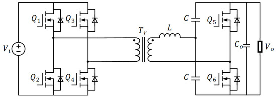
Figure 1.
Topology of the voltage-doubler-based SRDAB converter.
When the output filter capacitor is sufficiently large, the output voltage can be considered constant within one control cycle and is equivalent to a DC source. By referring the secondary-side voltage to the primary side, the equivalent circuit of the SRDAB converter is obtained, as shown in Figure 2. Due to the symmetry of the voltage-doubler structure, the effective transformer turns ratio is half that of a conventional SRDAB. In the high-frequency resonant path, two resonant capacitors C are connected in parallel on the secondary side. When referred to the primary side, the total resonant capacitance is , and the total resonant inductance is .
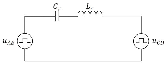
Figure 2.
Equivalent circuit of the voltage-doubler-based SRDAB converter.
Figure 3 illustrates the key waveforms under extended phase-shift (EPS) control. and denote the input and output DC voltages, respectively. and are the AC voltages across the primary and secondary bridge arms, is the resonant inductor current, is the switching frequency, and is the resonant frequency. The inner phase shift is denoted as , and the outer phase shift as .The normalized phase-shift ratios are defined as and . Under forward power flow, the ranges of and are and .
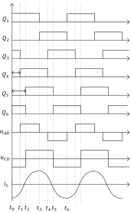
Figure 3.
Key waveforms of the voltage-doubler-based SRDAB under forward power flow.
2.2. Phasor-Time Domain Hybrid Modeling
In the equivalent circuit, the primary voltage can be decomposed into the sum of two square waves, each with amplitude , and phase angles of 0 and , respectively. The secondary voltage has an amplitude of . Using Fourier series expansion:
where . According to the superposition principle, instantaneous and average values of voltage, current, and power can be obtained by summing harmonic components. The phasor representation of the n-th harmonic is:
The n-th harmonic phasor of the inductor current is:
The complex power is given by:
where and are the active and reactive power of the n-th harmonic. The total output active power and reactive power are:
Let the characteristic impedance be and the frequency ratio . Neglecting losses, the output power is fully delivered to the load resistor , i.e., . Thus, the output voltage is:
To facilitate the subsequent numerical solution, the series can be summed up to obtain the time-domain expression of as follows:
The time-domain expression of the inductor current is obtained via inverse phasor transformation:
At key switching instants , , substituting into Equation (10) and summing the series yields the instantaneous inductor current:
The RMS value of the inductor current is:
where and are the RMS value and the maximum value of the n-th harmonic component of the inductor current.
3. Output Voltage Gain Correction Considering Dead Time and Parasitic Parameters
In practical applications, dead time is introduced to prevent shoot-through faults in power switches. However, this results in an effective duty cycle of the AC bridge voltages that is less than 50%, leading to inaccuracies in the voltage gain and current expressions derived under ideal square-wave assumptions.
Although a full time-domain segmentation of the - resonant process [21] could offer higher modeling precision, such an approach imposes significant computational overhead. Instead, we approximate the net impact of , the charge during dead time, as an equivalent reduction in active duty cycles, which is compensated via feedforward. Any residual deviation is effectively regulated by the closed-loop frequency controller, ensuring robust ZVS without requiring cycle-by-cycle harmonic analysis. Therefore, the output capacitance of power devices interacts with the inductor current during the dead time, generating a voltage variation . When the dead time is relatively large compared to , this voltage variation can sustain the bridge output level, causing a phase delay that effectively alters the phase-shift angle. Therefore, phase-shift compensation is necessary to improve model accuracy.
Taking the secondary-side driving signals as an example, as shown in Figure 4a, at time , if , the current charges , maintaining the negative voltage level during the dead time and resulting in a phase delay of . Similarly, at , if , the positive level is sustained, also introducing a delay of . Consequently, the effective outer phase shift becomes . In contrast, as shown in Figure 4b, when and , the current direction during dead time does not support voltage hold, resulting in no phase delay, and thus no compensation is required.
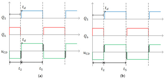
Figure 4.
Phase delay and voltage hold effect due to output-side dead time: (a) and . (b) and .
By analyzing the direction of inductor current at key switching instants and its impact on phase delay, a phase-shift compensation mechanism is established. Table 1 summarizes the phase delays and corresponding compensated output voltage expressions under forward power flow (where and ).

Table 1.
Phase delay and output voltage expressions after phase-shift compensation.
With the proposed compensation strategy, a more accurate prediction of the output voltage is achieved, laying the foundation for high-efficiency control design.
4. Efficiency Optimization Under Soft-Switching Conditions
4.1. Reactive Power and RMS Current Minimization
To achieve zero-voltage switching (ZVS) for power switches, the output capacitance must be fully discharged before the gate signal is applied, which requires the inductor current to be negative at turn-on, i.e., . Thus, ZVS feasibility can be evaluated using Equations (13) and (15):
Due to the complexity of the time-domain model of the voltage-doubler-based SRDAB, an analytical optimal solution is difficult to derive under Karush–Kuhn–Tucker (KKT) conditions. This paper adopts a numerical optimization approach: given fixed hardware parameters, the objective function is minimized subject to constraints such as ZVS conditions and output voltage regulation. The optimization results are then plotted and curve-fitted for practical implementation. The proposed method is applicable over wide input and output ranges. The following parameters are used for illustration: transformer turns ratio 1:4, resonant inductance µH, equivalent resonant capacitance µF, input voltage range 42–58 V, regulated output voltage (after dead-time compensation) V, and dead time ns.
First, reactive power minimization (as Equation (6)) is performed, and the results are shown in Figure 5. It can be observed that the inner phase-shift ratio is consistently zero, indicating that single-phase-shift control is sufficient for optimal performance. Moreover, the outer phase shift varies slightly across different load levels, which facilitates a unified control strategy from light to heavy loads.
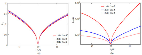
Figure 5.
Reactive power minimization results: (a) Variation in outer phase-shift ratio with . (b) Variation in switching frequency with .
Second, RMS current minimization (based on Equation (12)) is conducted, with the results shown in Figure 6. The analysis shows that remains zero, again validating the effectiveness of SPS control. However, varies significantly with load power, necessitating output current feedforward in closed-loop control to enhance the dynamic response.
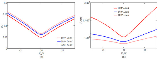
Figure 6.
RMS current minimization results: (a) Variation in outer phase-shift ratio with . (b) Variation in switching frequency with .
4.2. Minimization of RMS Switching Instantaneous Current
Although ensures ZVS for switch , a large current magnitude at turn-on leads to increased cross-conduction losses and significant reactive circulating current, degrading overall efficiency. To address this trade-off, this paper proposes a novel optimization objective: minimization of the root-mean-square (RMS) of the switching instantaneous current, defined as:
This metric comprehensively evaluates current stress at the three critical switching instants, aiming to balance ZVS feasibility with conduction loss minimization. The optimization results are presented in Figure 7. Key observations include:
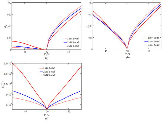
Figure 7.
RMS switching instantaneous current minimization results: (a) Variation in inner phase-shift ratio with . (b) Variation in outer phase-shift ratio with . (c) Variation in switching frequency with .
- At V, , and , the system operates near resonance in an open-loop manner, resembling an LLC resonant converter, achieving peak efficiency;
- When V, is close to zero, resulting in SPS-like behavior;
- When V, , equivalent to primary-side internal phase-shift control, similar to a phase-shift full-bridge (PSFB) converter.
4.3. Closed-Loop Control Design and Implementation
When and are fixed, the output voltage is a monotonically decreasing function of the switching frequency , as indicated by Equation (10). As shown in Figure 7, load power has a noticeable impact on and , requiring output current feedforward in closed-loop control for improved accuracy. Based on the above optimization, a closed-loop control scheme is proposed, as illustrated in Figure 8. The components are defined as follows:
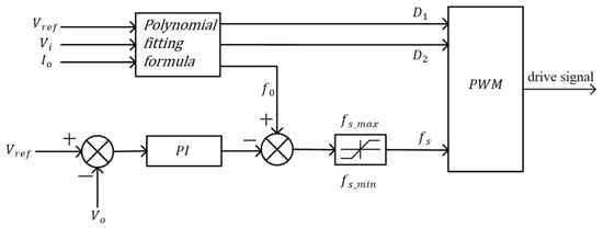
Figure 8.
Closed-loop control block diagram.
- : reference output voltage;
- : sampled output current;
- : phase-shift ratios and base frequency calculated online from fitted optimization curves;
- : minimum and maximum allowable switching frequencies.
The polynomial fitting formula is obtained by performing polynomial fitting on the optimized results of Figure 7 using Mathcad.The feedforward frequency command , derived from the fitting formula, is continuously updated based on real-time measurements of input voltage and output current . This adaptive feedforward mechanism plays a pivotal role in maintaining system robustness:
- During load transients, it proactively shifts the operating point to the new optimal frequency, minimizing the magnitude and duration of resonant current excursions;
- More importantly, it ensures ZVS for all power switches—even under worst-case step-load conditions.
Without this feedforward action, the feedback loop alone would respond too slowly to prevent temporary entry into the capacitive region, risking hard switching and potentially destructive spikes on the MOSFETs. The PI-based feedback loop thus operates as a fine-tuning element, correcting only minor modeling mismatches or disturbances, while the bulk of the dynamic response is handled by the physics-informed feedforward path.
5. Experimental Validation
5.1. Prototype Setup
To validate the proposed mathematical model, optimization methods, and control strategy, a 3 kW experimental prototype was built, as shown in Figure 9.
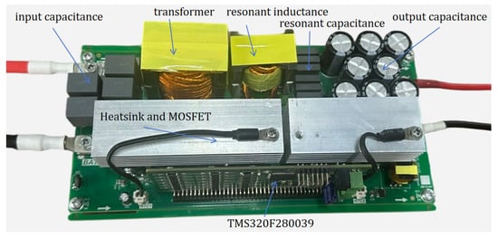
Figure 9.
Experimental prototype of the SRDAB converter.
The main circuit parameters are listed in Table 2.
Table 2.
Key parameters of the experimental prototype.
5.2. Soft-Switching Performance and Efficiency Evaluation
Figure 10 shows the gate-to-source voltage and resonant inductor current waveforms under 500 W and 2000 W output power, with V, at input voltages of 46 V and 54 V, respectively. It can be observed that: At turn-on of and , ; At turn-on of , ; indicating that all power switches achieve zero-voltage switching (ZVS). These results confirm that the proposed optimization-based control ensures reliable ZVS across wide input voltage and load ranges.
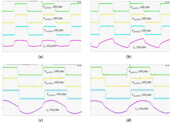
Figure 10.
Waveforms under different loads and different input voltages: (a) 500 W load and V. (b) 500 W load and V. (c) 1 kW load and V (d) 1 kW load and V.
To evaluate the accuracy of the proposed phasor-time domain hybrid model, it is compared with the conventional first-harmonic approximation (FHA) method. The phase-shift ratios and frequencies optimized using the corrected model are applied to the FHA-based model. The predicted, simulated, and measured output voltages are plotted in Figure 11. For each , the optimal , , and values are computed using the proposed model to achieve = = 400 V. These parameters are then applied to the experimental prototype, PSIM simulation, and FHA model. The resulting values are compared against the target 400 V to assess model accuracy and practical feasibility. It is evident that the corrected phasor-time model matches closely with both simulation and experimental results and exhibits significant deviation, especially under low-input or high-load conditions. This demonstrates the superior accuracy of the proposed model under non-ideal operating scenarios.

Figure 11.
Comparison of output voltage prediction accuracy among FHA, phasor-time domain hybrid model, simulation, and experiment.
Figure 12 presents the efficiency comparison among the three optimization strategies under 1 kW output power while varying from 42 V to 58 V. The results show that when V, the efficiencies of all three methods are similar; when V, the RMS switching instantaneous current minimization method achieves significantly higher efficiency; when V, its efficiency exceeds the other two by approximately 4%. These results validate the superiority of the proposed optimization objective in enhancing overall converter efficiency, particularly under high-input-voltage conditions.
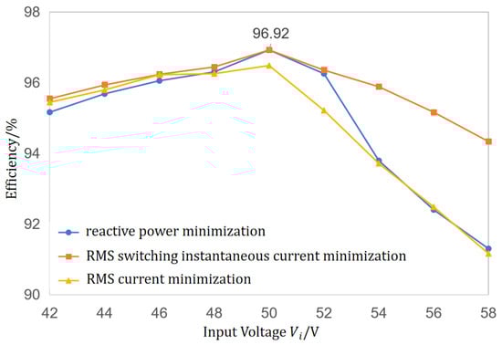
Figure 12.
The dynamic response process.
5.3. Dynamic Performance Validation
While steady-state efficiency is a key metric, the practical viability of the proposed control strategy hinges on its ability to maintain regulation, soft-switching, and device safety during transient events. To this end, comprehensive dynamic tests were conducted on the 3 kW prototype under both load-step and line-step conditions. The control architecture—featuring real-time feedforward of , , and based on measured and , augmented by a voltage-mode PI feedback loop—was rigorously evaluated.
The system was subjected to a full-load transient sequence ( = 45 V): 0 kW → 1 kW → 3 kW → 1 kW, with all key waveforms captured simultaneously using a digital oscilloscope. As shown in Figure 13, At time , the load steps from 0 kW to 1 kW, causing the output current to rise abruptly to 2.5 A. This results in a small undershoot in the output voltage of approximately 5% (20 V), which recovers to within ±1% of the 400 V reference in less than 100 ms. Subsequently, at time , the power demand increases further from 1 kW to the rated 3 kW. The output voltage exhibits the same undershoot of 5% (20 V) and settles back to the regulation band (±1%) in under 300 ms. Throughout both transients, the input voltage remains stable, confirming that the observed dynamics are solely due to load variation. Finally, at time , when the load steps down from 3 kW to 1 kW, the system demonstrates excellent damping with negligible overshoot and no oscillation, highlighting the robustness of the closed-loop controller.
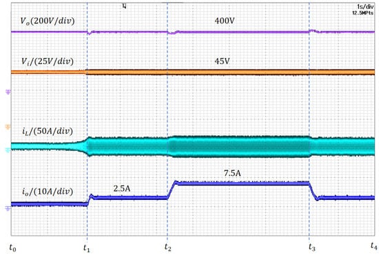
Figure 13.
Load transient response: 0 kW → 1 kW → 3 kW → 1 kW step at = 45 V.
Figure 14 shows the system response to a ±20% input voltage step (: 45 V → 55 V) at full load (3 kW). The output voltage deviation is limited to <3.5%, and the recovery time is under 150 ms. The resonant inductor current responds immediately to the increased input energy, exhibiting a small transient spike before stabilizing at its new operating level. Notably, the output current remains constant at 7.5 A throughout the transition, confirming precise power regulation and effective rejection of input disturbances.
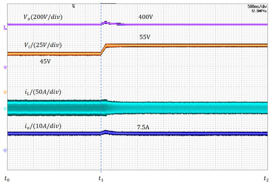
Figure 14.
Line transient response: step from 45 V to 55 V at 3 kW load.
6. Conclusions
This paper has proposed a phasor-time domain hybrid model for the voltage-doubler-based series-resonant dual-active-bridge converter under extended phase-shift control. The model incorporates the effects of dead time and power switch output capacitance on the output voltage gain, significantly improving modeling accuracy across wide input voltage and load ranges.Based on this model, three optimization objectives—reactive power, RMS current, and the proposed RMS of switching instantaneous current—are investigated under constraints of zero-voltage switching (ZVS) and regulated output voltage. A frequency-variable phase-shift control algorithm is then developed accordingly. The proposed modeling and control strategies are experimentally validated on a 3 kW prototype. The experimental results demonstrate that:
- 1.
- The proposed phasor-time domain model achieves high accuracy in predicting output voltage gain and ZVS conditions, closely matching both simulation and measurement data;
- 2.
- The RMS switching instantaneous current minimization strategy achieves higher overall efficiency compared to reactive power minimization and RMS current minimization, with up to 4% efficiency improvement under high-input-voltage conditions;
- 3.
- The proposed optimization and control method ensures reliable ZVS across wide voltage gain and load ranges, fully leveraging the soft-switching advantages of resonant DAB converters.
- 4.
- The real-time feedforward implementation enables fast and stable dynamic response under both load and line transients. Experimental waveforms show that the output voltage recovers from large steps (e.g., 1 kW → 3 kW) within less than 300 ms, with minimal overshoot/undershoot, and maintains regulation during ±20% input voltage variations, confirming the practical viability of the model-driven control approach.
Author Contributions
Conceptualization, Y.Z.; Methodology, Y.Z.; Software, Y.Z.; Validation, Y.Z.; Investigation, Y.Z.; Resources, J.L. (Jianhua Lei); Data curation, J.L. (Jingdou Liu); Writing—original draft, Y.Z.; Writing—review & editing, J.L. (Jianhua Lei) and L.J.; Visualization, J.L. (Jingdou Liu); Project administration, Y.Z. and J.L. (Jianhua Lei); Funding acquisition, J.L. (Jianhua Lei) and L.J. All authors have read and agreed to the published version of the manuscript.
Funding
This research was supported by the Shenzhen Science and Technology Program under Grant Number KJZD20230923112959001.
Data Availability Statement
The original contributions presented in this study are included in the article. Further inquiries can be directed to the corresponding author.
Conflicts of Interest
Author Yongbo Zhang and Jianhua Lei were employed by the company Institute of Renewable Energy, Shenzhen Poweroak Newener Co., Ltd. The remaining authors declare that the research was conducted in the absence of any commercial or financial relationships that could be construed as a potential conflict of interest.
References
- Li, Z.X.; Fan, G.Q.; Zhao, C.; Zhang, H.; Wang, P.; Li, Y. Research Review of Power Electronic Transformer Technologies. Proc. CSEE 2018, 38, 1274–1289. [Google Scholar] [CrossRef]
- Wang, Y.; Zheng, Z.; Li, Y. Review of Topology and Control Application of Medium and High Voltage Power Electronic Transformer. Adv. Technol. Electr. Eng. Energy 2017, 36, 1–10. [Google Scholar] [CrossRef]
- Shen, K.; Tong, P.; Hang, L.; Li, G.; Zhu, M.; Dai, R. Soft Switching Modulation Strategy of Dual Active Bridge Converters Applied in Renewable Energy Systems. Autom. Electr. Power Syst. 2019, 43, 154–159. [Google Scholar] [CrossRef]
- Zhao, B.; An, F.; Song, Q.; Yu, Z.; Zeng, R. Development and Application of DC Transformer Based on Dual-Active-Bridge. Proc. CSEE 2021, 41, 288–298. [Google Scholar] [CrossRef]
- Shao, S.; Chen, H.; Wu, X.; Zhang, J.; Sheng, K. Circulating Current and ZVS-On of a Dual Active Bridge DC-DC Converter: A Review. IEEE Access 2019, 7, 50561–50572. [Google Scholar] [CrossRef]
- Liu, H.; Mao, C.; Lu, J. Energy Storage System of Electronic Power Transformer and Its Optimal Control. Trans. China Electrotech. Soc. 2010, 25, 54–60. [Google Scholar]
- Xue, X.; Liu, Z.; Li, W.; Su, H. Design of a Single-Stage Dual Active Bridge Micro-Inverter with Wide Load Adaptability Based on Loss Optimization. IEEE Trans. Power Electron 2025, 40, 7919–7935. [Google Scholar] [CrossRef]
- Wu, H.; Sun, K.; Li, Y.; Xing, Y. Fixed-Frequency PWM-Controlled Bidirectional Current-Fed Soft-Switching Series-Resonant Converter for Energy Storage Applications. IEEE Trans. Ind. Electron. 2017, 64, 6190–6201. [Google Scholar] [CrossRef]
- Hao, C.; Lei, J.; Ma, H.; Guo, Z.; Qin, G. Phase-Shift Variable-Frequency Control Strategy of a Single-Stage Micro Inverter Based on Dual Active Bridge Topology. In Proceedings of the 2024 IEEE 12th International Conference on Smart Energy Grid Engineering (SEGE), Oshawa, ON, Canada, 18–20 August 2024; pp. 20–24. [Google Scholar] [CrossRef]
- Han, W.; Corradini, L. General Closed-Form ZVS Analysis of Dual-Bridge Series Resonant DC-DC Converters. IEEE Trans. Power Electron 2019, 34, 9289–9302. [Google Scholar] [CrossRef]
- Zhao, F.; Gan, Y.; Chen, X.; Wang, Y. Design of Dual Active Bridge Series Resonant Converter Based on Frequency Domain Analysis and Closed-Loop Control. High Volt. Eng. 2022, 48, 4557–4567. [Google Scholar] [CrossRef]
- Xiao, C.; Zhao, S. Minimum RMS Current Scheme of DAB Converter Based on Frequency Domain Analysis. Power Electron 2024, 58, 36–39. [Google Scholar] [CrossRef]
- Wu, J.; Cheng, Y.; Yan, X.; Sun, X. Power Loss of Series Resonant Three-Phase Dual Active Bridge Converter. Acta Energiae Solaris Sin. 2022, 43, 149–156. [Google Scholar] [CrossRef]
- Yaqoob, M.; Loo, K.H.; Lai, Y.M. A Four-Degrees-of-Freedom Modulation Strategy for Dual-Active-Bridge Series-Resonant Converter Designed for Total Loss Minimization. IEEE Trans. Power Electron. 2019, 34, 1065–1081. [Google Scholar] [CrossRef]
- Yang, B.; Ge, Q.; Zhao, L.; Zhou, Z. The Backflow Power Optimization of Dual Bridge Series Resonant DC/DC Converter. Proc. CSEE 2019, 39, 6990–6999. [Google Scholar] [CrossRef]
- Wu, J.; Li, Y.; Zhang, Z.; Wen, P.; Sun, X. Analysis on Soft-Switching Characteristics of Series Resonant Dual-Active-Bridge Converter. Acta Energiae Solaris Sin. 2017, 38, 3005–3011. [Google Scholar]
- Fan, E.; Li, Y.; Ge, Q. Feedforward Control Strategy of Dual Active Bridge Series Resonant Converter Based on Optimized Phase Shift. Trans. China Electrotech. Soc. 2025, 40, 5324–5333. [Google Scholar] [CrossRef]
- Gao, Y.; Zhou, Z.; Zhang, X.; Ma, H. Minimum Backflow Current Control of Under-Resonant Dual Bridge Series Resonant Converter. Trans. China Electrotech. Soc. 2024, 39, 4480–4494. [Google Scholar] [CrossRef]
- Wang, Q.; Sun, H.; Wang, C.; Wang, L. Optimal Control Strategy of DAB Converter Based on Frequency Domain Analysis. Power Electron. 2024, 58, 40–43. [Google Scholar] [CrossRef]
- Hu, Y.; Li, Z.; Zhao, C.; Luo, L.; Li, Y. Mechanism Analysis and Suppression of Oscillation in Dead Time of Series Resonant Dual Active Bridge Based on MOSFET. Trans. China Electrotech. Soc. 2022, 37, 2549–2558. [Google Scholar] [CrossRef]
- Xiao, Z.; He, Z.; Guan, R.; Luo, A. Piecewise-Approximated Time Domain Analysis of LLC Resonant Converter Considering Parasitic Capacitors and Deadtime. IEEE Trans. Power Electron. 2023, 38, 578–592. [Google Scholar] [CrossRef]
Disclaimer/Publisher’s Note: The statements, opinions and data contained in all publications are solely those of the individual author(s) and contributor(s) and not of MDPI and/or the editor(s). MDPI and/or the editor(s) disclaim responsibility for any injury to people or property resulting from any ideas, methods, instructions or products referred to in the content. |
© 2025 by the authors. Licensee MDPI, Basel, Switzerland. This article is an open access article distributed under the terms and conditions of the Creative Commons Attribution (CC BY) license (https://creativecommons.org/licenses/by/4.0/).