Abstract
Current manufacturing trends in 3D integration are resulting in a notorious increase in power density, and the use of conventional cooling methods may not be sufficient for cooling future 3D ICs with several chip dies. Moreover, with very thin chip dies, implementing alternative cooling methods based on etching microchannels in every chip die may not be technologically feasible. In this study, we suggest implementing microchannels only in the top, unthinned layer of silicon. In this case, the crucial parameter influencing cooling efficiency is the thermal conductance between vertically stacked chip dies. Therefore, an extensive numerical study is conducted, which quantifies the thermal performance of such single-layer microchannel heat exchangers as a function of inter-die thermal conductance, in addition to other chip parameters. Several important conclusions are presented based on these analyses. In particular, for various 3D stacks, this study allows the determination of the concrete threshold values of inter-die thermal conductance relative to which thermal performance degradation starts to become significant.
1. Introduction
To account for the need for ever-increasing processing power, chip manufacturers must constantly introduce new technological innovations. In particular, 3D integration [,] was proposed as one of the major breakthroughs that would allow Moore’s law to persist, placing an increasing amount of transistors into processing chips and resulting in higher computational power. At first, 3D-integrated chips were merely an idea suggested by scientists and researchers; however, recently, major semiconductor companies adopted the use of these chips in their products. Firstly, 2.5D integrated devices [] were considered; however, only in recent years has true 3D integration technology been fully adopted by chip manufacturers. The idea of 3D-integrated semiconductor devices, although scientifically and technologically complex and ambitious, is quite simple in principle. Instead of adding more transistors by increasing the chip’s footprint, another layer of silicon is added on top of the base layer, and vertical interconnections are used to facilitate communication between them.
The first 3D-stacked chips were DRAM memories [,], and it was only relatively recently that AMD revealed its use of V-cache—vertically stacked cache memory []—and Intel unveiled its Foveros technology for 3D integration []. It is only a matter of time before the processing cores are also stacked via several layers, although there are still several issues to be resolved: in particular, increasing the density of through-silicon vias (TSVs) [,] (which serve as interconnects between chip layers) and developing technology for the accurate bonding of chip layers [].
1.1. AMD’s 3D Processor Design with V-Cache
In this section, we present AMD’s Zen processors with first- and second-generation V-cache []. The first processor on the market that featured 3D cache technology, called first-generation V-cache, was AMD Ryzen 7 5800X3D, released in April 2022. Then, in November 2024, AMD unveiled Ryzen 7 9800X3D, which used second-generation V-cache. The layer stacking used in these two V-cache generations differ quite significantly, which reveals different approaches to handling interconnection complexity and thermal issues. It shows that even large companies and their researchers are actively looking for the optimal solution to stack two or more chip layers together.
Let us now briefly describe the technological steps undertaken in both Zen processor designs shown in Figure 1. During the manufacture of first-generation V-cache, the core die and V-cache die are thinned first; then, hybrid bonding [,,] is used to place V-cache on top of the core die. Hybrid bonding is a solderless bonding method that allows for an interconnect density of around 10,000 bonds per square millimeter, which is substantially higher than what is possible using microbumps []. The two dies are bonded face-to-back. Since the V-cache area is smaller, two “dummy” silicon blocks are oxide-bonded to the structure to fill the remaining area on top of the core die. To ensure structural stability, a thicker structural silicon layer is placed on top of V-cache die again using standard oxide bonding.
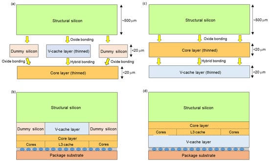
Figure 1.
Simplified bonding process for first-generation (a) and second-generation (c) V-cache technology (not to scale). Final design of the Zen processor with the V-cache layer on top of the core layer (b) and with the core layer on top of the V-cache layer (d) (not to scale).
The manufacturing process of the second V-cache generation is different: First, both the core die and V-cache are thinned and connected together—face-to-back again—but, this time, the core die is on top. In this generation, the V-cache area is the same as the core die area; thus, no “dummy” silicon blocks are used. Next, similarly to the previous approach, a thick layer of structural silicon is oxide-bonded on top of the stack.
Both designs have their advantages and issues, e.g., the first design is better in terms of routing complexity, as the connections between the PCB and the core die (including the entire power delivery network) do not have to be routed through the V-cache die. However, the first design suffers from worse cooling properties, as the power generated in the core die has to pass through two oxide bonding layers instead of one, increasing the thermal resistance of this heat flow path and therefore exacerbating the chip’s temperature issues. It can therefore be presumed that even AMD engineers are not entirely sure which approach is better; thus, they opted to test two different designs and evaluate their processing power and thermal performance in practice. Moreover, the answer to the question of whether it is advantageous to place the core die on top of the stack may change in the future if more dies are added to the 3D stack. This decision will also heavily depend on the value of the inter-die thermal conductance, i.e., on thermal conductivity and the thickness of the interface between chip dies.
1.2. Microchannel Heat Exchanger as Future Solution for Cooling 3D Processors
The increase in power density due to 3D stacking pushes conventional cooling solutions to their limits. Therefore, microchannel cooling [,], which offers substantially lower chip thermal resistance, was proposed as a potential solution. Previous studies have explored material and topology optimization strategies for conventional microchannel heat sinks []. In contrast, the present study focuses on embedded microchannels etched directly in silicon. The fluid absorbs heat from the chip, which is then removed to the outside due to the flow of the fluid. The entire heat transfer mechanism is described in detail by the authors of []. Most importantly, microchannel cooling typically offers an order of magnitude higher cooling efficiency with respect to forced air convection.
The other important advantage of microchannel-based cooling is its potential scalability: Most researchers considered implementing microchannels in all the dies of a 3D chip [,]. Consequently, since, for every additional die, both the total dissipated power and cooling efficiency would increase, it would guarantee that the peak chip temperature could stay theoretically constant even if more dies are added. However, we would like to challenge this view and show that placing microchannels in every die of the chip, while of course offering many advantages, might not be sound from a technological perspective. The reason is that the most important goal for chip manufacturers is to provide dense and fast interconnections between chip dies [], which means that the TSV density needs to be very high. This, in turns, means that the TSV diameter has to be as small as possible. Since the manufacture of TSVs is currently limited by their aspect ratio [], achieving small-diameter TSVs means that they also need to be as short as possible, and therefore, the chip dies should also be as thin as possible. For example, in AMD’s Zen processor, the thickness of the core dies is below 20 µm. Thus, it may be simply unrealistic to manufacture sufficiently large microchannels in such thin dies, considering also that the large areas of these dies will have to be reserved for implementing TSVs. Recall that microchannel cooling performance quickly decreases if the wetted area decreases, and this effect cannot really be compensated by only increasing the fluid velocity because the pressure drop would become prohibitive []. Consequently, even if it was technologically possible to etch small microchannels in sub-20 µm dies, their cooling performance might not be sufficient for cooling future 3D-stacked chips.
1.3. Inter-Die Thermal Conductance in 3D ICs
One of the most crucial parameters that determines the thermal performance of 3D ICs is the inter-die’s thermal conductance. Its importance is even greater in the case of single-layer cooling systems, such as the one analyzed in this study, because the heat generated in the chip’s lower dies has to pass through all upper dies to reach the heat exchanger. Therefore, the lower the conductance, the higher the temperatures reached in the chip—especially in the bottommost die.
In this study, inter-die thermal conductance refers to the effective vertical conductance through the back end of line (BEOL) of the lower die and the bonding interface up to the active silicon of the upper die (Figure 2). In the case of Zen processors, the hybrid bonding manufacturing process ensures that the resulting bond will be very thin; thus, its conductance will be high. Consequently, the BEOL layer’s thermal conductance will be the dominant factor in the total inter-die thermal conductance. The problem is that the BEOL’s layer conductance is very difficult to estimate. Even knowing the layer’s thickness and the exact properties of the materials used may not be enough to precisely calculate the resulting thermal conductance. The reason is that this layer is composed not only of a dielectric but also of many metal interconnections. Additionally, the simplest approach of calculating the effective thermal conductivity only based on the dielectric/metal ratio can result in a vastly overestimated value, as most metal interconnections are horizontal, and vertical interconnections usually do not span across the entire layer. It is also worth mentioning that, in future 3D ICs, BEOL conductance may be artificially increased by implementing dedicated thermal vias [,,], which render it even more difficult to realistically estimate its value. Taking the above into consideration, we decided to use the value of inter-die thermal conductance as the most important variable parameter in this study, i.e., most results are calculated as a function of variable inter-die thermal conductance.
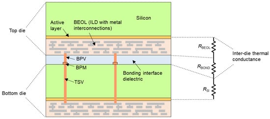
Figure 2.
Illustration of the inter-die thermal conductance parameter used in this study (not to scale). TSV: Through-silicon via; BPM: bond pad metal; BPV: bond pad via; ILD: inter-layer dielectric. RBEOL, RBOND, and RSI denote the thermal resistances of the BEOL layer, bonding interface, and silicon layer, respectively.
1.4. Motivation
In this study, we propose a single-layer microchannel heat exchanger as a potential solution for cooling future 3D ICs. The main idea is that microchannels are present only in the topmost, thicker layer of silicon, which allows them to be larger, with heights up to hundreds of micrometers. The reason why the topmost die can be left unthinned (unlike other dies) is that there are no TSVs that need to be etched through this die. Let us consider, for example, both Zen processor designs shown in Figure 1: A structural silicon die is implemented on top to ensure the mechanical stability of the structure. It would be perfectly possible to etch large microchannels in this die before bonding it to the chip, creating an efficient microchannel heat sink. However, since this solution is not scalable and microchannels are located only in the top silicon layer, there are important questions to be answered: How effective will the cooling of this single-layer microchannel be with respect to the inter-die’s thermal conductance? How effective will it be as the number of stacked dies in the chip is increased? Can only applying a faster fluid flow be a sufficient solution to these issues?
Therefore, in this study, we present a thorough examination of the effectiveness of single-layer microchannel cooling in 3D stacked processors, not only taking into account inter-die thermal conductance but also many other design parameters, namely the number of chip layers, fluid velocity, and power distribution. Additionally, we analyze and provide conclusions about how the cooling efficiency changes depending on particular layer stackings—e.g., how much better it is from a thermal perspective to place the core die (with high power density) closer to microchannels while positioning the cache die (with low power density) farther away.
In comparison to our previous research [], the following analysis is more exhaustive. In our previous study, COMSOL Multiphysics was used as a simulation tool, which limited the scope of analyses due to long finite element method (FEM) simulation times. Additionally, to shorten simulation times, a simple structure with only 10 channels was analyzed. This approach, while sound in general, might not adequately reflect how complex chips with more microchannels will behave. Therefore, the analysis presented in this study is much more detailed because it uses a substantially faster [] simulation tool and is able to take many more parameters into consideration and carry out simulations within a reasonable time frame using a 3D chip with a large number of microchannels. Unlike previous research, this study also focuses uniquely on a single-layer microchannel chip design. Finally, the main focus of this study is the impact of inter-die thermal conductance, which was a fixed parameter in our previous study.
2. Simulation Methodology
2.1. Simulation Tool
The TIMiTIC tool was used during this study. A thorough description of its features and capabilities can be found in another publication []. In brief, the 3D-stacked chip is discretized in space into multiple nodes connected via thermal resistances, for which their values are calculated based on material properties and their respective dimensions. Similarly, every node’s capacitance is calculated based on the node’s dimensions and the respective material’s specific heat and density. TIMiTIC is then used to solve Equation (1), where T is the vector of temperatures in each node, C is the vector of thermal capacitances at each node, G is the matrix of thermal conductances between each pair of nodes, and Q is the vector of heat source powers at each node. In other words, each element in the matrix Gij represents the thermal conductance between nodes i and j. Each element Ci represents the thermal capacitance of node i, while each element Qi represents the power dissipated at node i. In this study, every chip die was divided into 40 × 40 nodes, which translates to 1600 nodes per die. This size was chosen as a trade-off between accuracy and simulation speed: It was determined that increasing the grid’s resolution does not significantly affect the final temperature values. Additionally, to account for thermal resistances due to bonding and BEOL layers, thermal contacts were added between chip dies. Moreover, free convection was simulated at the top and bottom of the chip; however, it should be emphasized that its impact on the final results is minimal, as the amount of heat removed through convection is negligible compared to that removed via fluid flow. The remaining chip side walls are considered in the model as adiabatic surfaces. As for the fluid domain, 40 microchannels were added to the model. Similarly to the chip dies, every microchannel was discretized into 40 nodes, which resulted in 1600 model nodes representing fluid temperatures along all 40 microchannels. It is worth pointing out that the TIMiTIC tool allows for a detailed simulation of the fluid domain, including all thermal entry effects and variable Nusselt numbers along the channels (more information is published by the authors of []). The resulting model representing the analyzed chip has the form of a 3D network of thermal resistances. For this network, a well-known matrix equation with conductance and heat source matrices can then be created. Note that, in the following study, only steady-state analysis is used; therefore, Equation (1) is reduced to its time-independent form, and only a linear system of equations based on matrix G and vector Q needs to be solved. It is also worth mentioning that the temperature-controlled heat sources shown in Figure 3, which are used for modeling heat transfer due to fluid flow, can be included in Equation (1) as elements of the thermal conductance matrix G. The linear system is solved using a dedicated eigenSparseLU algorithm []. The typical TIMiTIC steady-state simulation time of a 3D stack discretized into dozens of thousands of nodes is typically very fast—in the range of several hundred milliseconds:
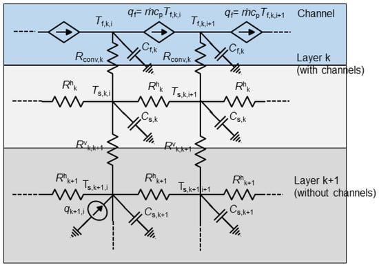
Figure 3.
A fragment of the mathematical model simulated using TIMiTIC []. Note that the full model is three-dimensional, but in this figure, it is presented in two dimensions for clarity. Tf: fluid temperature at a given node; Ts: solid temperature at a given node; Rh: horizontal thermal resistance; Rv: vertical thermal resistance; Rconv: convection resistance between solid and fluid; Cf: fluid node capacitance; Cs: solid node capacitance: q: heat source power; qf: heat flow due to advection; : mass flow; cp: fluid specific heat.
2.2. Simulated 3D Processor Stack
The general structure of the 3D stack used in this study is shown in Figure 4, and it is based on AMD’s Zen processor design. As complete information about this design is not available, some parameters had to be assumed. The entire chip has an area of 15 mm × 15 mm. At the bottom of the stack, two or more chip dies are present, each with a height of 20 µm. Thermal contacts between chip dies are introduced to account for the additional thermal resistance between dies due to bonding and BEOL layers. The topmost silicon die is unthinned, has a height of 600 µm, and is oxide-bonded on top of the last chip die. It contains 40 straight microchannels, each measuring 250 µm × 400 µm in cross-section, stretching across the entire length of the chip. The inlet fluid temperature is fixed at 300 K and is used as a reference for the calculation of temperature increases in other locations. The inlet fluid velocity is a variable parameter in the analysis. The fluid–solid convection mechanism is simulated as thermal resistances between the solid and the fluid, and each resistor value is calculated based on the heat transfer coefficient (HTC) in the respective microchannel area. The Hausen correlation [] (adapted to rectangular channels) is used to calculate the Nusselt numbers as a function of the distance from the inlet, which are needed to calculate all HTCs along all channels. The movement of the fluid is simulated by temperature-controlled heat sources added to the model, and their parameters are calculated based on fluid properties and velocity. The heat spreader layer and thermal interface layer (TIM) were also included in the model because, from the thermal perspective, the heat spreader may be useful for rendering the chip’s temperature more spatially uniform. However, it should be noted that the impact of these two layers on the conclusions presented in this study is most likely minimal. The summary of all simulation parameters is provided in Table 1. The boundary conditions are listed in Table 2.
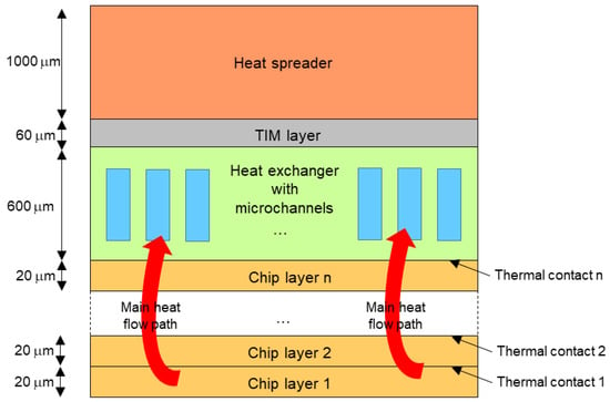
Figure 4.
The structure of the simulated 3D-stacked processor (not to scale).

Table 1.
Parameters of the simulated 3D-stacked processor.

Table 2.
Boundary conditions used in simulations.
3. Results and Discussion
3.1. Analysis 1: The Impact of Inter-Die Thermal Conductance on Temperatures for Variable Inlet Fluid Velocity
In this section, two designs, Z1 and Z2—as shown in Figure 5—are compared. In both designs, the processor is composed of two dies: the core/cache die and the V-cache die. The only difference between the designs is the positioning of cores and V-cache in the 3D stack; in the Z1 design, the cores are located at the bottom of the stack, while in the Z2 design, the cores are located at the top, close to the microchannel’s heat exchanger. The Z1 design is a better solution from the perspective of implementing interconnections and routing, but the Z2 design is likely to be superior from a thermal perspective. In what follows, we attempt to quantify how the Z2 design is better compared to the Z1 design in terms of thermal performance. Figure 6 shows the positioning of cores, caches, and V-cache in the chip with respect to microchannels.
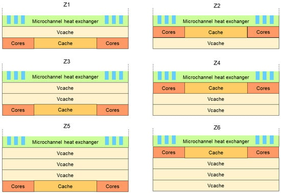
Figure 5.
Vertical cross-section of six simulated 3D processor stacks (Z1–Z6)—not to scale. Some chip layers are hidden for clarity (see Figure 4 for the complete simulated 3D stack).
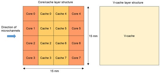
Figure 6.
The horizontal organization of layers in simulated 3D processor stacks.
Figure 7 shows the maximum chip temperature increase as a function of inter-die thermal conductance (expressed in W/(m2 K)) for three cases of inlet fluid velocity values—0.2 m/s, 0.3 m/s, and 0.5 m/s, which correspond to around 0.95 kPa, 1.42 kPa, and 2.37 kPa of pressure drop, respectively. The bottom horizontal curves represent the results for the design in which processor cores are located at the top of the stack (closer to the microchannels), while the top curves are the results for the design in which processor cores are located at the bottom of the stack. Curves of the same color (green, blue, or orange) represent the results for the same case of inlet fluid velocity. The first observation is that, as expected, increasing the fluid velocity reduces the maximum chip temperature. For example, for high inter-die thermal conductance, the maximum chip temperature increase was lowered by 16 K from 60 K to 44 K, when the velocity was changed from 0.2 m/s to 0.5 m/s. However, this occurs with diminishing returns; thus, it may be postulated that the highest reduction in temperatures occurs when advection resistance is the dominant part of the total chip’s thermal resistance. As fluid flow velocity is increased and advection resistance decreases, solid–fluid convection resistance starts to dominate, and an increase in flow velocity does not produce temperature reductions that are as high compared to before.
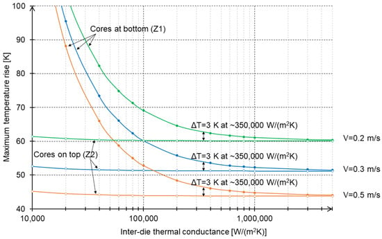
Figure 7.
Maximum chip temperature increase as a function of inter-die thermal conductance for various fluid inlet velocities.
A second observation is that if cores are on top of the stack and close to the microchannels, the impact of the inter-die thermal conductance of the bonding layers on chip temperatures is minimal. This is also a logical outcome, as the power dissipated in the “buried” V-cache layers is substantially lower than the one dissipated in cores; thus, the relatively small heat flow from the bottom die—impeded by the increased thermal resistance—does not significantly affect the peak temperatures. On the other hand, in the case of the other design—with cores located at the bottom of the stack—the large heat flow from cores has to pass through the bonding/BEOL layer before it can be absorbed by the fluid; consequently, the impact of inter-die thermal conductance in this case is significant, as evidenced by sharply rising curves in the figure.
Third, a comparison of curves of the same color allows us to observe how the “cores on top” design is better from a thermal standpoint than the “cores at bottom” design. The temperature penalty for placing cores at the bottom of the 3D stack increases with the inter-die’s thermal conductance, and it is virtually the same regardless of the fluid velocity. However, it should be noted that if the inter-die’s thermal conductance stays within reasonable limits, this penalty is quite low. For example, assuming that the acceptable penalty for placing cores at the bottom of the stack is 3 K, then this method is feasible as long as thermal contact conductance is above 350,000 W(m2 K); moreover, this value should be achievable in 3D IC manufacturing processes. Consequently, a conclusion that is very counterintuitive is reached: From a thermal perspective, it may not be important where cores are located in a 3D stack of two layers, as the peak temperature difference between these two solutions does not exceed 3 K, as long as inter-die thermal conductance is reasonably high. This suggests that it may be preferable to place the cores at the bottom of the stack to facilitate routing and reduce the total wire length at the cost of only slightly higher temperatures. However, it should be emphasized that this conclusion is valid for 3D stacks with two dies only, and it may change if more dies are added to the 3D stack. Such an analysis is provided in the next section.
3.2. Analysis 2: The Impact of Inter-Die Thermal Conductance on Temperatures for Variable Number of Chip Dies
In this section, all designs Z1–Z6 are compared in terms of their thermal performance (Figure 8). Unlike the previous section, the fluid velocity is fixed at 0.5 m/s for all designs (which corresponds to around 2.37 kPa of pressure drop). The 3D stacks Z3 and Z4 are composed of one core/cache die and two V-cache dies. In 3D stacks Z5 and Z6, there is one core/cache die and three V-cache dies. The power dissipation of each die is also fixed; thus, the designs with more dies have higher power dissipation. As a result, the designs should be compared only with respect to the following pairs: Z1 with Z2; Z3 with Z4; and Z5 with Z6. As one might have expected, with an increase in the number of dies, designs Z1/Z3/Z5 exhibit increasingly worse thermal performance, while that for designs Z2/Z4/Z6 remains relatively stable. Let us assume again that 3 K is the maximum acceptable temperature penalty for placing cores at the bottom of the stack. For the Z1/Z2 pair, this means that the inter-die’s thermal conductance needs to be at least 350,000 W/(m2 K). However, for designs Z3/Z4 with two V-cache dies, this requirement is more strict, as the inter-die’s thermal conductance must be at least 680,000 W/(m2 K). With even more dies (designs Z5/Z6), the 3 K penalty requirement is met only when inter-die thermal conductance is above 1,000,000 W/(m2 K). In other words, from the thermal perspective, design Z5 should be considered over design Z6 only if the thermal contacts between bonded chip dies have conductance values higher than 1,000,000 W/(m2 K), which would then result in a 3 K increase in peak chip temperature. Achieving this inter-die thermal conductance value for bonding/BEOL layers in future 3D manufacturing technologies may be a difficult challenge, but it is feasible if manufacturing technology is improved and/or high-density thermal vias are implemented.
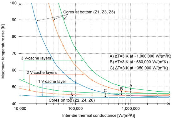
Figure 8.
Maximum chip temperature increase as a function of inter-die thermal conductance for different numbers of V-cache dies on the chips.
While analyzing the results, it may be postulated that the reason why thermal performance degrades quite quickly for Z1/Z3/Z5 designs is because the vast majority of power is dissipated in the core die, located at the very bottom of the stack. This is obviously true; consequently, additional simulations were carried out to determine whether thermal performance improves when the power dissipation ratio between cores and caches is lower. The results are shown in the next section.
3.3. Analysis 3: The Impact of Inter-Die Thermal Conductance on Temperatures for Various Core/Cache Power Dissipation Breakdowns
In this section, only Z5 and Z6 designs with three V-cache dies are analyzed. Two power distributions are considered: the default distribution—with 100 W dissipated in cores and 14 W in caches—and the new distribution—84 W of power dissipated in cores and 28 W in caches. Note that total power therefore stays constant and equals 114 W. The results are presented in Figure 9. Contrary to what could be expected, doubling the power in caches and reducing power consumption in cores only has a minor effect on the conclusions drawn in the previous section. The thermal conductance requirement for choosing the Z6 design over the Z5 design was reduced only from 1,000,000 W/(m2 K) to 900,000 W/(m2 K). Since the real core-to-cache power consumption ratio in future 3D processors is unlikely to be higher than the one considered in this study, one may conclude that the power breakdown between cores and cache does not have a significant influence on thermal performance, as long as this power breakdown stays within realistic limits. One interesting aspect that can be observed in the results is that the two bottommost curves have a crossing point. Indeed, when inter-die conductance is high (right part of the graph), the dominant factors influencing the peak temperature are core areas with the highest power density. Therefore, the design with 100 W dissipated in cores exhibits higher maximum temperatures than the design with only 84 W dissipated in cores. However, as inter-die conductance decreases (left part of the graph), the chip’s peak temperature is determined by the heat dissipated at the bottom V-cache layers, exhibiting a very high thermal resistance path for reaching the microchannels. Therefore, the design with higher power (3 × 8 W) dissipated in V-caches begins to exhibit a higher peak temperature than the design with lower power (3 × 4 W) dissipated in V-caches.
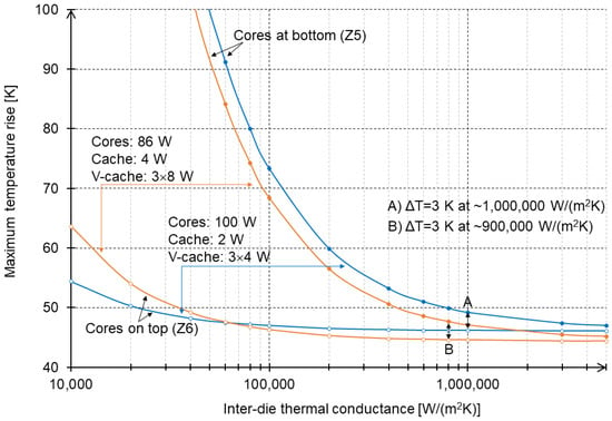
Figure 9.
Maximum chip temperature increase as a function of inter-die thermal conductance for two core/cache power distributions.
3.4. Analysis 4: The Impact of Inter-Die Thermal Conductance on Temperatures for Different Vertical Arrangements of Core and V-Cache Dies
In previous sections, only 3D processors with one core die were analyzed. Since core areas dissipate the majority of power, adding more core dies will drastically increase total power dissipation and could potentially alter the chip’s thermal behavior. In this section, four new processor designs (F1–F4: see Figure 10) are analyzed. All designs contain two core/cache dies and two V-cache dies, but their mutual vertical positioning is different in every design. In the F1 design, the cores are located in the bottommost layers, and both V-cache dies are at the top of the stack. This design may be optimal from a routing perspective, as it minimizes the number of interconnections that have to be routed vertically through the chip; this is because most chip interconnections are present between the package substrate and processor cores. However, from the thermal perspective, this solution is, of course, the worst, as areas with high power dissipation are located far from the microchannel heat exchanger. The features of the F2 design are exactly the opposite: It would require complex routing to connect the topmost core dies to the package substrate, but simultaneously, this design minimizes the thermal resistance between the cores and microchannels. Designs F3 and F4 are intermediate solutions between the two previous designs: The core and V-cache dies are stacked interchangeably in the chip. These solutions are better in terms of thermal performance compared to the F1 design, but they are also worse in terms of routing.
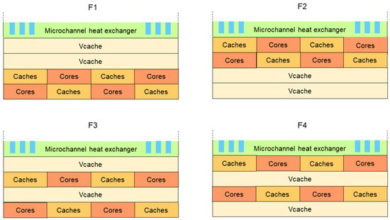
Figure 10.
Vertical cross-section of four simulated 3D processor stacks with two core dies (F1–F4)—not to scale. Some common chip layers are hidden for clarity (see Figure 4 for the complete simulated 3D stack).
Note that when two core dies are present in the chip instead of one, the mutual positioning of cores in both dies can have a substantial impact on the resultant temperatures. If the cores were stacked on top of each other, their power density would effectively culminate, producing hot spots in the chip. Therefore, a more logical solution is to use different arrangements of cores/caches in each die such that the cores in one die are located on top of caches in the other die (and vice versa) (Figure 11). It was confirmed via simulations that this horizontal positioning of dies produces the lowest peak temperatures; therefore, this arrangement is taken into account in the following analysis. Moreover, since the chip dissipates much more power compared to designs from the previous sections, the fluid inlet velocity was increased to 1 m/s (which corresponds to around 4.75 kPa of pressure drop) in these simulations to maintain chip temperatures at a reasonable level.
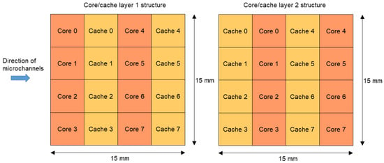
Figure 11.
The horizontal organization of chip dies in simulated 3D processor stacks with two core dies.
At first glance, the results are unsurprising, with the F1 design exhibiting the worst results and the F2 design demonstrating the best thermal performance. However, upon closer inspection, an unexpected observation can be made: As long as the conductance of the bonding/BEOL layer is not lower than 1,000,000 W/(m2 K), the peak temperatures for all designs are fairly similar, with differences not exceeding 2 K (Figure 12). This suggests that if chip manufacturers can ensure sufficiently high inter-die thermal conductance, the vertical positioning of dies in the 3D stack will have little impact, provided that a 2 K increase in peak temperature is acceptable. Only when the inter-die thermal conductance drops below 1,000,000 W/(m2 K) do more significant peak temperature differences between designs appear—for example, reaching 4.7 K for 400,000 W/(m2 K).
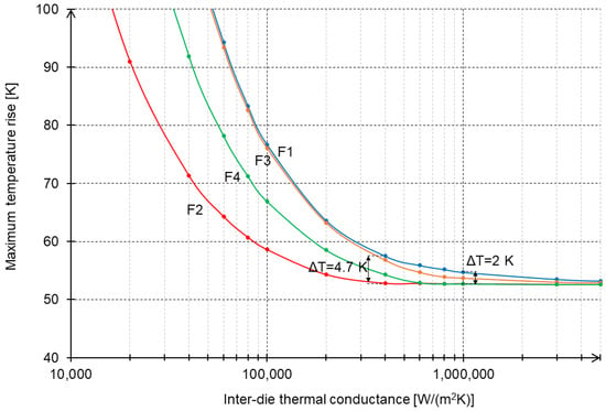
Figure 12.
Maximum chip temperature increase as a function of inter-die thermal conductance for designs F1–F4 with two core dies.
The same set of simulations was also repeated for various values of fluid velocity. Obviously, the faster the flow, the lower the observed peak temperatures. However, as the temperature differences between different designs were very similar to those shown in Figure 12, the results are not presented in this study. Ultimately, one may conclude that changing fluid velocities does not influence the conclusions drawn from the comparisons of the designs presented in this section.
A careful observer may also notice a strange phenomenon in the results shown in Figure 12. In some areas, the curves overlap, i.e., the maximum temperature increase is the same for two different designs, which may suggest a mistake in the model or the simulation’s setup. However, after careful analyses, it was confirmed that the data are correct, and the phenomenon results from the chip’s normal thermal behavior. The analysis of this phenomenon and its explanation is provided in the next section.
3.5. Analysis 5: The Impact of Inter-Die Thermal Conductance on the Intensity of Local Temperature Hot Spots
A decision was made to plot the chip temperatures along the cross-section through the bottommost die—from the inlet side to the outlet side—for F1–F4 designs and for the two following cases: when the inter-die thermal conductance is high and when it is relatively low. Recall that the designs and the positioning of cores and caches in each die are shown in Figure 10 and Figure 11. Any cross-section of the chip’s bottom die, taken from the inlet side to the outlet side, passes through four chip areas—designated here as areas A1–A4. Every area is located under a partial stack of the same chip units (one core, one cache, and two V-caches), but for each design, these units are vertically positioned according to different orders (see Figure 13).
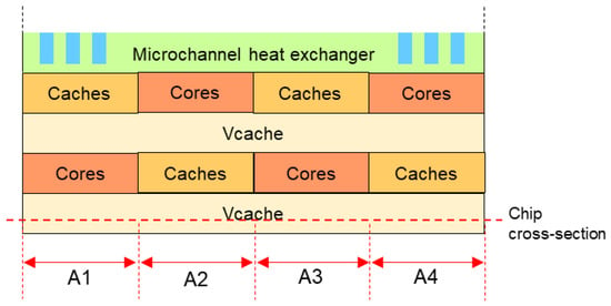
Figure 13.
Illustration of the analyzed chip cross-section with marked A1–A4 areas based on design F4. Cross-sections for other designs are created according to a same manner.
If the thermal conductance between dies is relatively high, heat flows freely between them. As shown in Figure 14, temperatures are very similar across all designs, although small differences in areas A1–A4 can be easily observed. These differences result from the fact that, for every area, the vertical positioning of units corresponding to the given area is different. Let us analyze one example for clarity. In the F4 design, above areas A1–A4, there are two V-cache units, one core unit, and one cache unit. However, for areas A1 and A3, the cores are “buried” deeper than the caches, and for areas A2 and A4, the opposite is true. This explains the slight changes in the shape of the curves in Figure 14 when transitioning between areas.
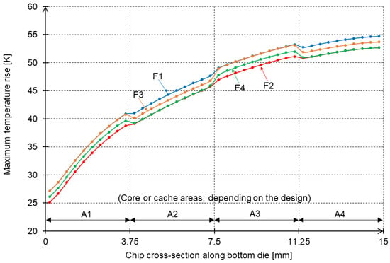
Figure 14.
Maximum chip temperature increase in the bottom chip layer along the chip’s cross-section for cases of high inter-die thermal conductance (1,000,000 W/(m2 K)). See the text for an explanation of the A1–A4 areas.
Additionally, one can observe that the temperatures increase almost monotonically from the inlet side to the outlet side; consequently, the highest temperature increase in the bottom chip die occurs at the outlet side (on the extreme right of the graph). However, in the case of low inter-die thermal conductance, the cross-sectional temperatures are very different (Figure 15). In this case, due to the high thermal resistance between dies, heat becomes trapped in the “buried” dies, and visible local hot spots occur in areas A1 and A3, i.e., the areas in which cores are “buried” deeper than caches. As a result, the maximum chip temperature increase occurs not at the outlet side of the chip but in area A3, corresponding to the local temperature hot spot.
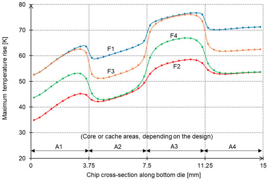
Figure 15.
Maximum chip temperature increase in the bottom chip layer along the chip’s cross-section for cases of low inter-die thermal conductance (100,000 W/(m2 K)). See the text for an explanation of the A1–A4 areas.
The reason for the strange phenomenon observed in Figure 12 becomes clear. For high inter-die thermal conductance values, the maximum temperature increase in the chip occurs with respect to the bottommost die at the far outlet side. Its value depends almost uniquely on the total sum of powers dissipated in the A4 area. Since this sum is the same for all designs, the temperature increase for all designs is similar, and in the case of designs F2 and F4, the increase is almost identical. However, as the inter-die thermal conductance decreases below 600,000 W/(m2 K), the maximum temperature increase occurs at the local hot spot in the A3 area, and its value is primarily determined by the cores’ power density. This explains why the local hot spot temperatures of designs F1 and F3 in Figure 15 are the same, which translates to the same peak temperature increases for the designs in Figure 12 with respect to low inter-die thermal conductances.
4. Conclusions
In this study, a dedicated tool for the thermal simulation of 3D ICs cooled by microchannels was employed to quantify the impact of inter-die thermal conductance on the thermal performance of 3D-stacked processors. The analyzed chip designs were based on AMD’s Zen processor with two chip dies and extrapolated into future 3D ICs with multiple dies. Numerous important findings were discovered, which may be useful not only for researchers but also for future chip designers. The most important conclusions from the study are listed below.
Analysis 1 showed that, for 3D chip stacks with two layers, the design with a core die located at the bottom of the stack is a valid alternative to the design with a core die located closer to the heatsink. As long as the inter-die thermal conductance is above 350,000 W/(m2 K), the penalty for placing cores at the bottom of the stack (in terms of increased peak temperature) may be considered low (below 3 K). Our conclusion is also independent of the fluid velocity used.
Analysis 2 allowed the estimation of the minimum inter-die conductance value, which guarantees that the increased peak temperature does not exceed 3 K for 3D stacks with more chip dies. For example, for a chip with four stacked dies, the minimum inter-die conductance has to be at least 1,000,000 W/m2 K in order to satisfy this requirement.
Analysis 3 proved that the conclusions provided by the previous analysis remain valid for any realistic power dissipation breakdown between the core and caches.
Analysis 4 showed that for 3D stacks with two core dies and two V-cache dies, their vertical positioning has far less impact on their resulting peak temperatures than what may be intuitively expected. In particular, if the inter-die thermal conductance is above 1,000,000 W/(m2 K), the peak temperature exhibited by each of the four analyzed designs differs at most by 2 K. Additionally, if the inter-die thermal conductance is above 400,000 W/(m2 K), then the same temperature difference is at most 4.7 K.
Analysis 5 proved that low inter-die thermal conductance values not only cause an increase in overall chip temperatures due to an increase in the chip’s thermal resistance but also result in the occurrence of local hot spots, which increase the peak temperature of the chip even further.
In conclusion, this study emphasizes the importance of achieving the highest possible inter-die thermal conductance, for example, by keeping the bonding/BEOL layers as thin as possible or by implementing dedicated areas filled with thermal vias. The benefits extend beyond simply decreasing the chip’s thermal resistance; our analysis shows that it also mitigates the impact of local temperature hot spots. Moreover, if the thermal conductance between dies is maintained at a high level (typically above 1,000,000 W/(m2 K) for 3D stacks with four dies), it relaxes constraints on the positioning of core/cache dies, giving chip designers more flexibility. Consequently, rather than being constrained by thermal concerns, designers can focus more on other challenges, such as more efficient routing and minimizing power dissipation in chip interconnections.
It should be noted that all conclusions stated in this study are based solely on simulations of chips with at most four core/cache dies with 20 µm thickness. Consequently, for 3D ICs with more dies or substantially thicker dies, thermal performance may degrade more rapidly, and a stricter requirement on the minimum value of inter-die thermal conductance may be needed.
Author Contributions
Conceptualization, P.Z. and W.Z.; methodology, P.Z.; software development, P.Z. and W.Z.; validation, P.Z.; investigation, P.Z.; collection of data, P.Z.; writing—original draft preparation, P.Z.; writing—review and editing, P.Z. and W.Z.; supervision, P.Z. and W.Z. All authors have read and agreed to the published version of the manuscript.
Funding
This research received no external funding.
Data Availability Statement
The simulation tool is publicly available for download at timitic.dmcs.pl. The configuration and result files are available from the authors upon request.
Conflicts of Interest
The authors declare no conflicts of interest.
References
- Beyne, E. The 3-D Interconnect Technology Landscape. IEEE Des. Test 2016, 33, 8–20. [Google Scholar] [CrossRef]
- Sharma, R. Design of 3D Integrated Circuits and Systems; CRC Press: Boca Raton, FL, USA, 2014. [Google Scholar]
- Zhang, X.; Lin, J.K.; Wickramanayaka, S.; Zhang, S.; Weerasekera, R.; Dutta, R.; Chang, K.F.; Chui, K.J.; Li, H.Y.; Wee Ho, D.S.; et al. Heterogeneous 2.5D integration on through silicon interposer. Appl. Phys. Rev. 2015, 2, 021308. [Google Scholar] [CrossRef]
- Kim, J.; Kim, Y. HBM: Memory solution for bandwidth-hungry processors. In Proceedings of the 2014 IEEE Hot Chips 26 Symposium (HCS), Cupertino, CA, USA, 10–12 August 2014; pp. 1–24. [Google Scholar] [CrossRef]
- Sohn, K.; Yun, W.J.; Oh, R.; Oh, C.S.; Seo, S.Y.; Park, M.S.; Shin, D.H.; Jung, W.C.; Shin, S.H.; Ryu, J.M.; et al. A 1.2 V 20 nm 307 GB/s HBM DRAM With At-Speed Wafer-Level IO Test Scheme and Adaptive Refresh Considering Temperature Distribution. IEEE J. Solid-State Circuits 2017, 52, 250–260. [Google Scholar] [CrossRef]
- Wuu, J.; Agarwal, R.; Ciraula, M.; Dietz, C.; Johnson, B.; Johnson, D.; Schreiber, R.; Swaminathan, R.; Walker, W.; Naffziger, S. 3D V-Cache: The Implementation of a Hybrid-Bonded 64MB Stacked Cache for a 7nm x86-64 CPU. In Proceedings of the 2022 IEEE International Solid-State Circuits Conference (ISSCC), San Francisco, CA, USA, 20–26 February 2022; Volume 65, pp. 428–429. [Google Scholar] [CrossRef]
- Ingerly, D.B.; Amin, S.; Aryasomayajula, L.; Balankutty, A.; Borst, D.; Chandra, A.; Cheemalapati, K.; Cook, C.S.; Criss, R.; Enamul, K.; et al. Foveros: 3D Integration and the use of Face-to-Face Chip Stacking for Logic Devices. In Proceedings of the 2019 IEEE International Electron Devices Meeting (IEDM), San Francisco, CA, USA, 7–11 December 2019; pp. 19.6.1–19.6.4. [Google Scholar] [CrossRef]
- Lu, T.; Serafy, C.; Yang, Z.; Samal, S.K.; Lim, S.K.; Srivastava, A. TSV-Based 3-D ICs: Design Methods and Tools. IEEE Trans. Comput.-Aided Des. Integr. Circuits Syst. 2017, 36, 1593–1619. [Google Scholar] [CrossRef]
- Abdullah, M.; Lee, H. Technology review of CNTs TSV in 3D IC and 2.5D packaging: Progress and challenges from an electrical viewpoint. Microelectron. Eng. 2024, 290, 112189. [Google Scholar] [CrossRef]
- Kim, J.; Zhu, L.; Torun, H.M.; Swaminathan, M.; Lim, S.K. Micro-bumping, Hybrid Bonding, or Monolithic? A PPA Study for Heterogeneous 3D IC Options. In Proceedings of the 2021 58th ACM/IEEE Design Automation Conference (DAC), San Francisco, CA, USA, 5–9 December 2021; pp. 1189–1194. [Google Scholar] [CrossRef]
- Evers, M.; Barnes, L.; Clark, M. The AMD Next-Generation “Zen 3” Core. IEEE Micro 2022, 42, 7–12. [Google Scholar] [CrossRef]
- Elsherbini, A.; Liff, S.; Swan, J.; Jun, K.; Tiagaraj, S.; Pasdast, G. Hybrid Bonding Interconnect for Advanced Heterogeneously Integrated Processors. In Proceedings of the 2021 IEEE 71st Electronic Components and Technology Conference (ECTC), Virtual, 1 June–4 July 2021; pp. 1014–1019. [Google Scholar] [CrossRef]
- Arnaud, L.; Moreau, S.; Jouve, A.; Jani, I.; Lattard, D.; Fournel, F.; Euvrard, C.; Exbrayat, Y.; Balan, V.; Bresson, N.; et al. Fine pitch 3D interconnections with hybrid bonding technology: From process robustness to reliability. In Proceedings of the 2018 IEEE International Reliability Physics Symposium (IRPS), Burlingame, CA, USA, 11–15 March 2018; pp. 4D.4-1–4D.4-7. [Google Scholar] [CrossRef]
- Kim, Y.; Kim, J.; Kim, H.; Lee, H.; Kim, D.; Seo, S.K.; Jo, C.; Kim, D.W. Die to Wafer Hybrid Cu Bonding for Fine Pitch 3D-IC Applications. In Proceedings of the 2023 IEEE 73rd Electronic Components and Technology Conference (ECTC), Orlando, FL, USA, 30 May–2 June 2023; pp. 1043–1047. [Google Scholar] [CrossRef]
- Kim, S.W.; Detalle, M.; Peng, L.; Nolmans, P.; Heylen, N.; Velenis, D.; Miller, A.; Beyer, G.; Beyne, E. Ultra-Fine Pitch 3D Integration Using Face-to-Face Hybrid Wafer Bonding Combined with a Via-Middle Through-Silicon-Via Process. In Proceedings of the 2016 IEEE 66th Electronic Components and Technology Conference (ECTC), Las Vegas, NV, USA, 31 May–3 June 2016; pp. 1179–1185. [Google Scholar] [CrossRef]
- Guo, F.; Suo, Z.J.; Xi, X.; Bi, Y.; Li, T.; Wang, C.; Su, K.; Zou, X.; Li, R. Recent Developments in Thermal Management of 3D ICs: A Review. IEEE Access 2025, 13, 94286–94301. [Google Scholar] [CrossRef]
- Wang, S.; Yin, Y.; Hu, C.; Rezai, P. 3D Integrated Circuit Cooling with Microfluidics. Micromachines 2018, 9, 287. [Google Scholar] [CrossRef] [PubMed]
- Bianco, N.; Cherella, N.; Fragnito, A.; Iasiello, M.; Mauro, G.M. Multi-material topology optimization of innovative microchannel heat sinks equipped with metal foams. Int. J. Heat Mass Transf. 2024, 222, 125201. [Google Scholar] [CrossRef]
- Zając, P. Compact Thermal Modelling Tool for Fast Design Space Exploration of 3D ICs with Integrated Microchannels. Energies 2020, 13, 2217. [Google Scholar] [CrossRef]
- Brunschwiler, T.; Michel, B.; Rothuizen, H.; Kloter, U.; Wunderle, B.; Oppermann, H.; Reichl, H. Forced convective interlayer cooling in vertically integrated packages. In Proceedings of the 2008 11th Intersociety Conference on Thermal and Thermomechanical Phenomena in Electronic Systems, Orlando, FL, USA, 28–31 May 2008; pp. 1114–1125. [Google Scholar] [CrossRef]
- Shi, B.; Srivastava, A.; Bar-Cohen, A. Co-design of micro-fluidic heat sink and thermal through-silicon-vias for cooling of three-dimensional integrated circuit. IET Circuits Devices Syst. 2013, 7, 223–231. [Google Scholar] [CrossRef]
- Wang, J.; Duan, F.; Lv, Z.; Chen, S.; Yang, X.; Chen, H.; Liu, J. A Short Review of Through-Silicon via (TSV) Interconnects: Metrology and Analysis. Appl. Sci. 2023, 13, 8301. [Google Scholar] [CrossRef]
- Chen, X.; Chen, Z.; Xiao, L.; Hao, Y.; Wang, H.; Ding, Y.; Zhang, Z. Fabrication and Electrical Characterization of High Aspect Ratio Through-Silicon Vias with Polyimide Liner for 3D Integration. Micromachines 2022, 13, 1147. [Google Scholar] [CrossRef] [PubMed]
- Biswal, L.; Chakraborty, S.; Som, S.K. Design and Optimization of Single-Phase Liquid Cooled Microchannel Heat Sink. IEEE Trans. Components Packag. Technol. 2009, 32, 876–886. [Google Scholar] [CrossRef]
- Ren, Z.; Alqahtani, A.; Bagherzadeh, N.; Lee, J. Thermal TSV Optimization and Hierarchical Floorplanning for 3-D Integrated Circuits. IEEE Trans. Components Packag. Manuf. Technol. 2020, 10, 599–610. [Google Scholar] [CrossRef]
- Qu, C.; Dai, R.; Zheng, J.; Hu, Y.; Zhang, J. Thermal and mechanical reliability of thermal through-silicon vias in three-dimensional integrated circuits. Microelectron. Reliab. 2023, 143, 114952. [Google Scholar] [CrossRef]
- Cong, J.; Zhang, Y. Thermal via planning for 3-D ICs. In Proceedings of the ICCAD-2005, IEEE/ACM International Conference on Computer-Aided Design, San Jose, CA, USA, 6–10 November 2005; pp. 745–752. [Google Scholar] [CrossRef]
- Zając, P.; Janicki, M.; Napieralski, A. On the applicability of single-layer integrated microchannel cooling in 3D ICs. In Proceedings of the 2018 19th International Conference on Thermal, Mechanical and Multi-Physics Simulation and Experiments in Microelectronics and Microsystems (EuroSimE), Toulouse, France, 15–18 April 2018; pp. 1–6. [Google Scholar] [CrossRef]
- Zając, P. TIMiTIC: A C++ based Compact Thermal Simulator for 3D ICs with Microchannel Cooling. In Proceedings of the 2019 25th International Workshop on Thermal Investigations of ICs and Systems (THERMINIC), Lecco, Italy, 25–27 September 2019; pp. 1–6. [Google Scholar] [CrossRef]
- Guennebaud, G.; Jacob, B.; Avery, P.; Bachrach, A.; Barthelemy, S. Eigen v3. Available online: http://eigen.tuxfamily.org (accessed on 3 June 2024).
- Bennett, T.D. Correlations for the Graetz problem in convection—Part 1: For round pipes and parallel plates. Int. J. Heat Mass Transf. 2019, 136, 832–841. [Google Scholar] [CrossRef]
Disclaimer/Publisher’s Note: The statements, opinions and data contained in all publications are solely those of the individual author(s) and contributor(s) and not of MDPI and/or the editor(s). MDPI and/or the editor(s) disclaim responsibility for any injury to people or property resulting from any ideas, methods, instructions or products referred to in the content. |
© 2025 by the authors. Licensee MDPI, Basel, Switzerland. This article is an open access article distributed under the terms and conditions of the Creative Commons Attribution (CC BY) license (https://creativecommons.org/licenses/by/4.0/).