Article

A Limited Common-Mode Current Switched-Capacitor Multilevel Inverter Topology and Its Performance and Lifetime Evaluation in Grid-Connected Photovoltaic Applications

1
Electrical and Computer Engineering Faculty, University of Tabriz, Tabriz 51666, Iran
2
School of Electrical Engineering, Shandong University, Jinan 250031, China
3
Department of Electronics Design, Mid Sweden University, 85170 Sundsvall, Sweden
4
Department of Energy Technology, Aalborg University, DK-9220 Aalborg, Denmark
*
Author to whom correspondence should be addressed.
Energies 2021, 14(7), 1915; https://doi.org/10.3390/en14071915
Submission received: 4 March 2021 / Revised: 24 March 2021 / Accepted: 26 March 2021 / Published: 30 March 2021
(This article belongs to the Special Issue Power Electronics for the Grid Integration of Photovoltaic Systems)

Abstract

:
In this paper, a switched-capacitor multilevel inverter with voltage boosting and common-mode-voltage reduction capabilities is put forth. The proposed inverter is synthesized with one-half bridge and several switched-capacitor cells. Due to the voltage boosting and common-mode current reduction features, the proposed multilevel inverter is suitable for grid-connected PV applications. In addition, an analytical lifetime evaluation based on mission profile of the proposed inverter has been presented to derive lifetime distribution of semiconductors. Whereas in the proposed inverter, any components failure can bring the whole system to a shutdown. The series reliability model is used to estimate the lifetime of the overall system. The performance of the suggested multilevel inverter in grid-connected applications is verified through the simulation results using the grid-tied model in Matlab/Simulink. Moreover, the viability and feasibility of the presented inverter are proven by using a one kW lab-scaled prototype.

1. Introduction

Recently solar energy has gained more attention since it is clean, emission-free, and easy to install. However, the voltage produced by these resources is low and requires a voltage booster stage, either a dc-dc stage or a transformer [1]. Conventionally in photovoltaic (PV) grid-connected inverters for safety issues, a line frequency transformer or a high-frequency transformer is used to ensure the galvanic isolation within the utility grid and PV array and also to boost the input voltage. The line frequency transformers are bulky and have low efficiency and high cost. High-frequency transformers have lower volume, weight, and cost but require extra power stages and extra elements that complicate the system and, more importantly, impair inverter efficiency [2]. To increase efficiency and power density and reduce cost and weight, transformers are excluded from PV systems. Elimination of the transformer may lead to some consequences such as requiring high voltage in the input of the inverter and ground leakage current that flow through parasitic capacitors between the PV terminals and grounded panel frame [3]. The leakage current leads to some anomalies such as the increment of output current total harmonic distortion (THD), increment of power losses, PV panel degradation, and electric shock. In order to use transformer-less inverters in industrial applications and ensure system safety, several solutions to suppress the leakage current have been investigated, which are generally based on two main ideas. The first one is based on the idea of decoupling PV and grid during freewheeling operation modes that result in eliminating high frequency (switching frequency) variant common-mode voltage. Derivations of the H-bridge inverter such as H5 [4], OH5 [5], H6 with ac bypass [6], H6 with dc bypass [7], and HERIC [8] inverters, use the power decoupling concept in the ac or dc side. However, the decoupling solution cannot be completely executed due to the parasitic capacitors of active switches. Thus, the leakage current still exists in the mentioned solutions. Furthermore, in the mentioned solution, two identical filter inductors with independent cores are needed that causes an increase in the size and cost [9]. The second solution is to directly clamp the voltage of PV terminals, which is more successful at mitigating the leakage current. Topologies like half-bridge inverter, NPC, and ANPC [10] inverters suppress current flow in parasitic capacitors by grounding the middle point of the dc-link. Doubly grounded topologies, which are also known as common-ground inverters, also clamp parasitic PV capacitors by connecting one terminal of PV array to the ground of the utility grid in order to eliminate leakage current completely [11].
Multilevel converters surpass two-level or three-level converters on account of better output quality. Moreover, the multilevel converters have low voltage stress on components, smaller filter requirement, low EMI, and lower switching loss [12,13,14]. In addition, these converters are used when voltage matching is required. Many multilevel topologies have been presented in the literature. Although they offer many advantages in some industrial applications, usually they cannot mitigate the leakage current and are not suitable for grid-connected PV applications.
In this paper, a switched-capacitor multilevel inverter (SC-MI) for PV application is put forth. The proposed topology is composed of several basic modules. Each basic module is synthesized with two capacitors, two switches, and two diodes. The topology uses solely one dc source as the input source. The common mode current in the proposed topology oscillates with the grid frequency thus the leakage current is effectively alleviated in grid-tied applications with the suggested multilevel inverter. Since the proposed inverter is synthesized with switched-capacitor cells, the voltages of the capacitors are balanced spontaneously without using any auxiliary circuit. The other advantage of the proposed inverter is that it draws a continuous current from the input. Detection of the weakest components in the suggested inverter using the presented reliability analyses is an indispensable part of the reliability-based design to lower the risks of semiconductor devices during operation [15,16,17]. Since the electrical and thermal stresses of the semiconductor devices change through the inverter, a method is required to consider the variable stresses on the semiconductor devices, which is called mission-profile based lifetime estimation [18,19]. Detail of the used lifetime estimation approaches is discussed in the following parts of this paper.

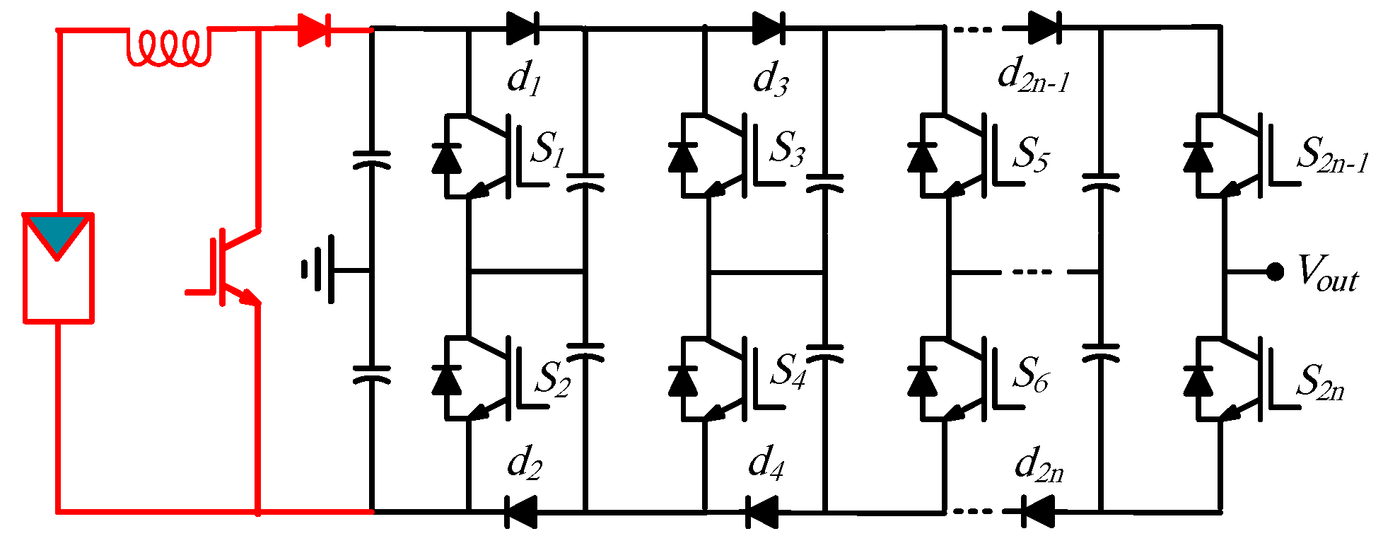
2. Structure and Operational Principle

2.1. Proposed Topology with N Stages

The presented inverter was composed of one half-bridge and several basic modules. The basic module, which was combined with a pair of capacitors, switches, and diodes, is illustrated in Figure 1a,b, and shows the general configuration of the proposed SC-MI.

2.2. Operational Principle

An eight-level structure of the proposed multilevel inverter topology illustrated in Figure 2 was taken into consideration to define how various voltage levels were created and capacitors voltage were balanced. To this end, the on and off status of the semiconductor components and charging/discharging states of the capacitors were indicated in Table 1. In this table, “C”, “D”, and “F” indicated the charging, discharging, and floating states of the capacitors, respectively. Moreover, “1” and “0” show the on and off states of the semiconductors, accordingly.
For the sake of more clarity, the current paths of the voltage levels must be derived. In addition, the charging paths of the capacitors can prove that the capacitors are charging and discharging equally. Figure 3 can cover the mentioned aims. In these figures, the output current paths are shown in black, and the charging current paths of the capacitors are colored in red.

3. Voltage Boosting and Leakage Current Suppression Features

As mentioned before, the proposed multilevel inverter can boost the output voltage through the switched-capacitor cells. Assuming the input voltage is Vdc and n is the switch legs count, the peak value of the output of the proposed inverter can be given as:
V p e a k = V d c k = 1 n 2 k 2 ,
Because the input cell (half-bridge) in the proposed topology provides a mid-point, the capacitance of the parasitic capacitance of the input dc source (PV panel) was added to the input capacitors, as shown in Figure 4. Whereas the voltages across the input capacitors (Cu1 and Cl1) oscillate with the grid frequency, which was a low frequency, the common-mode voltage across these capacitors was low. Thus, the common-mode current (leakage current) that stems from the common-mode voltage oscillation was insignificant in the proposed inverter topology. The voltages across the input capacitors include some dc and ac content, these components are as follows:
V C u 1 = V d c 2 + Δ V a c ,
V C l 1 = V d c 2 Δ V a c ,
Considering that the input capacitors are the same (Cu1 = Cl1 = C) and knowing that the load current is a pure sinusoidal current with the peak value, angular frequency, and lagging phase delay of Im, ω, and φ, accordingly, the oscillation content of the input capacitors voltage is obtained as
Δ V a c = I m C ω cos ( ω t φ ) ,
Whereas the common-mode current stems from the voltage oscillation across the parasitic capacitors, this current is given as:
I c m = ( C p v 1 + C p v 2 ) d V C u 1 ( l 1 ) d t ,
where Cpv1 and Cpv2 are the parasitic capacitors of the input dc source (PV panel).
Through Equations (4) and (5), the common-mode current is obtained as
I l e a k a g e = I m ( C p v 1 + C p v 2 ) 2 C sin ( ω t φ ) ,
Referring to the latter equation and knowing that the parasitic capacitors are so tiny in comparison with the input capacitors, the common-mode current was insignificant in the proposed multilevel converter.
The voltage across the capacitors varies, thus; the output voltage can experience a voltage drop at the output side. In order to provide precise voltage amplitude, a front-end boost converter can be used at the input side. This boost converter can compensate for the voltage drop, filter out the input current harmonics, and facilitate the MPPT. This point should be mentioned that, whereas the mentioned voltage drop is low, the front-end boost converter will only operate with a tiny duty cycle to make up the voltage drop and facilitate the MPPT. Figure 5 illustrates the suggested inverter, which is integrated with a front-end boost converter. The output voltage of such a configuration is obtained as
V p e a k = V d c 1 d k = 1 n 2 k 2 ,
As shown in Equation (7), the peak value of the output voltage can be modulated by manipulating the duty cycle (d).

4. Power Loss Calculation

In this section, the power losses of the presented converter are investigated. Generally, the power losses of the converters mainly consisted of conduction losses and switching losses. Conduction power loss occurs as a result of on-state resistance and semiconductors voltage and also the capacitors’ equivalent series resistance (ESR).
For an eight-level configuration, considering the power factor of unity, the on-state voltage and resistance per level are equal to:
R n = { R 1   =   R d   +   E S R   + R s w l   =   0.5 V d c R 2   =   R d   +   2 E S R   +   2 R s w l   =   1.5 V d c R 3   =   R d   +   2 E S R   +   2 R s w l   =   2.5 V d c R 4   =   3 E S R   +   3 R s w l   =   3.5 V d c
V o n , s = { V o n 1   =   2 V o s , d   +   V o s , s w l   =   0.5 V d c V o n 2   =   V o s , d   +   2 V o s , s w l   =   1.5 V d c V o n 3   =   V o s , d   +   2 V o s , s w   l   =   2.5 V d c V o n 4   =   3 V o s , s w   l   =   3.5 V d c
The total conduction loss of the converter can be figured out by:
P l o s s _ c o n d u c t i o n = f ( n 1 4 4 R n i ( t ) 2 d t + n 1 4 4 V o n , n i ( t ) d t ) ,
where, Rd, Rsw, ESR, l, Vdc, f, i(t), Von,d and Von,sw are the diode on-state resistance, diode switch on-state resistance, diode capacitor equal series resistance, diode voltage level, diode input voltage, diode frequency of output voltage, diode instantaneous load current, diode voltage drop value of a diode in conduction mode, and diode voltage drop value of a switch in conduction mode, respectively.
The switching losses, as its name suggests, appear during turning on and off of the semiconductors due to the overlap of voltage and current of the switch. For an eight-level configuration, the switching power loss of each switch is given as
P s 1 , 2 = 0.5 C s V d c 2 f s ,
P s 3 , 4 = 2 C s V d c 2 f s ,
P s 5 , 6 = 8 π C s V d c 2 f s sin 1 ( 1 7 ) ,
Thus, the total switching loss of an eight-level configuration is achieved as:
P s = C s V d c 2 f s ( 5 + 8 π sin 1 ( 1 7 ) ) ,
where Cs and fs are output capacitance of a switch and switching frequency, respectively.

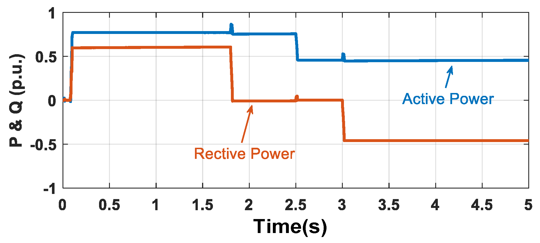
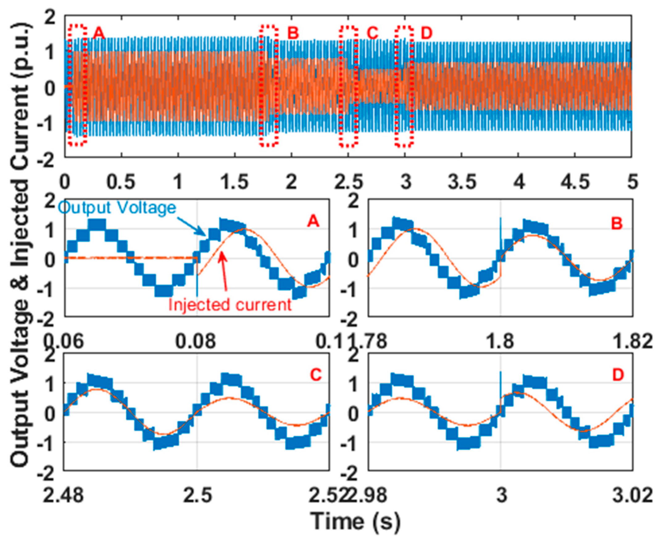
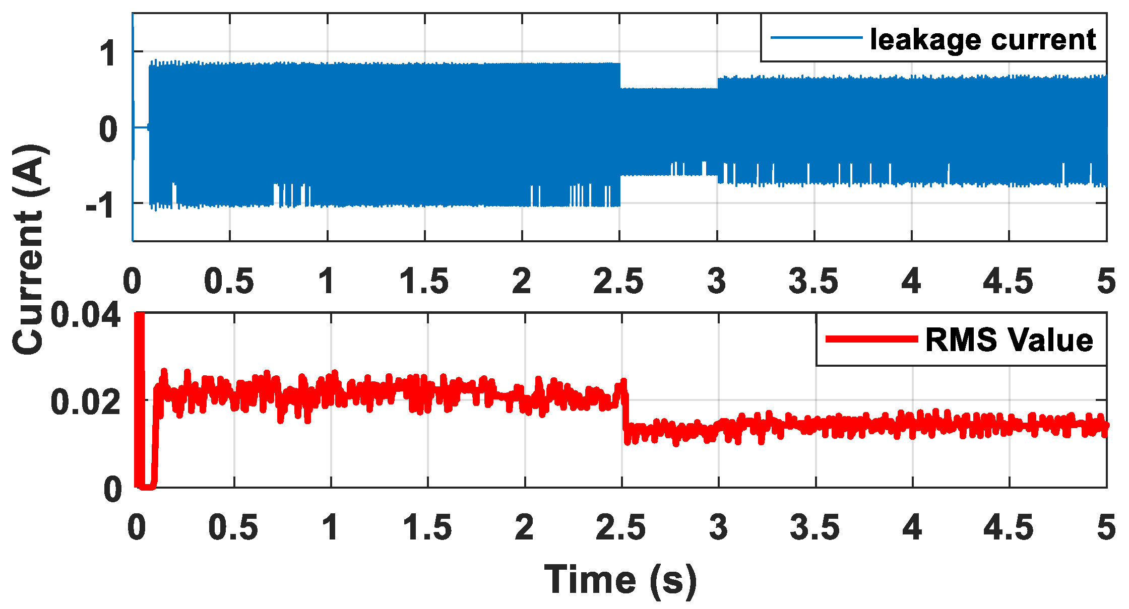
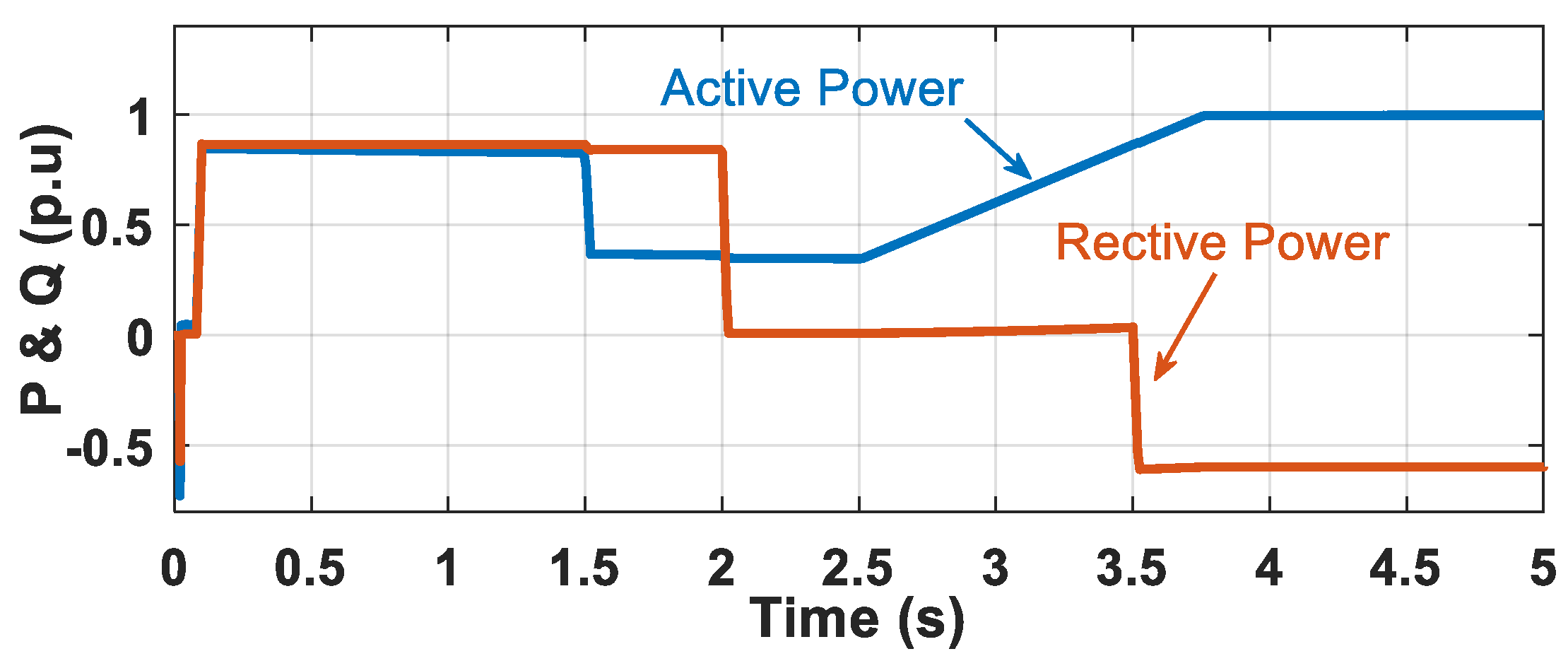
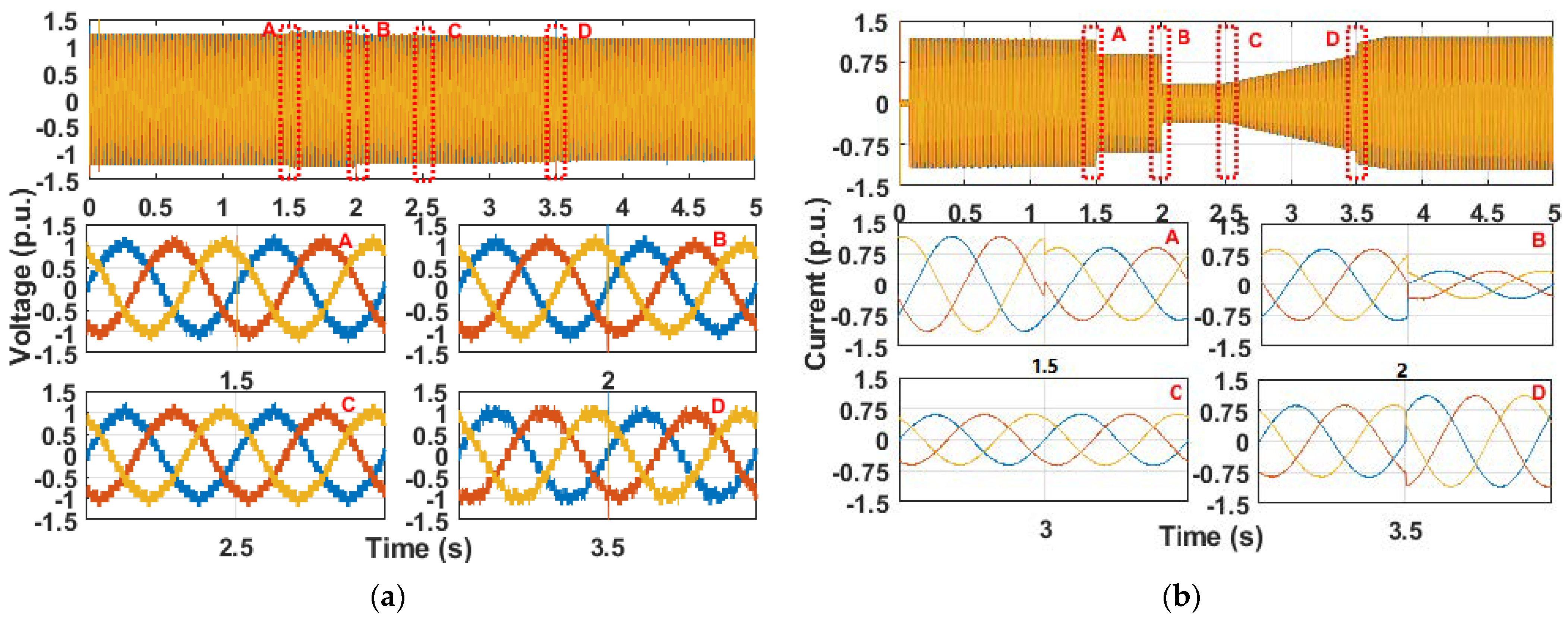
5. Simulation Results of Grid-Tied Mode

In order to assess the performance of the suggested structure in grid-tied PV application, considering the characteristic that is reported in Table 2, it was tested in Matlab/Simulink by assuming various loading conditions. In this investigation, several scenarios were considered for reactive power.
In order to inject the active power and exchange the reactive power in grid-tied mode, the ac components of the grid were transferred to the d-q axis components. The MPPT unit gives the reference of DC-link voltage. A Proportional Integral (PI) controller was used to keep the DC voltage into the desired value and develop the reference for the active power. The reactive power reference can be adjusted according to specialized control approaches. By using the active and reactive power references and obtaining the d- and q-axis voltages, the references of the output current can be ascertained. By having the parameters at hand, the reference output voltage was obtained. The reference voltage was used to derive the switching signal of the switches. The described control approach is shown in Figure 6.
The provided active and reactive powers are shown in Figure 7. As is depicted in Figure 7, the gate signals were blocked to allow the capacitors to be charged through the grid up to t = 80 ms. The active power of 0.77 p.u. (5 kW) was injected into the grid from t = 80 ms to t = 2.5 s. The injected power decreased to 0.46 p.u (3 kW) at t = 2.5 s. Moreover, three scenarios were considered for the reactive power. In the first scenario, the reactive power was considered 0.55 p.u. from t = 8 ms to t = 1.8 s. It decreased to zero and −0.5 p.u at t = 1.8 s and t = 3 s, respectively. As evident in Figure 7, the suggested converter had successfully operated in lagging and leading power factors.
The output voltage should be shown together with the injected current under the indicated conditions. Thus, the mentioned parameters are illustrated in Figure 8. As shown, the inverter developed a boosted high-quality ac voltage (Vg_peak 325 V) from a low voltage PV module (135 V). According to Figure 8, since the inverter operated in lagging power factor, the current was 35.57 degrees behind the output voltage from t = 80 ms to t = 1.8 s. The inverter operates in purely resistive loading conditions from t = 1.8 s to t = 2.5 s, thus the current was in phase with the output voltage. The active power decreased to 0.5 p.u. at t = 2.5 s, thus the amplitude of the injected current decreased. The reactive power decreased to −0.5 p.u. at t = 3 s. Thus the inverter operated at the leading power factor, and the injected current was ahead of the output voltage by 45 phase degree.
In order to evaluate the quality of the injected current, the fast Fourier transform (FFT) technique was employed to derive Figure 9. As illustrated, the THD of the injected current was under the rated value (according to the IEEE 4715 the maximum measured THD of the injected current is to be under 5%).
For completing the single-phase grid-tied investigations, the capability of the converter to mitigate the leakage current was also tested. To this end, a 300 nF stray capacitor was connected within the PV module and grid ground. The results are exhibited in Figure 10. As shown, the Root Mean Squire (RMS) value was around 20 mA, which was distinctly lower than the assigned value (according to VDE 0126-0101 standard, the leakage current should be under 300 mA).
The viability of the three-phase eight-level structure of the proposed topology in grid-connected mode was also investigated in this section. The base apparent power was considered 15 kVA, and the base phase voltage (peak value) was considered 320.
The provided active and reactive powers are exhibited in Figure 11. As shown, the presented converter had successfully supplied the reactive while transferred active power. Thus, the three-phase configuration can properly satisfy the VDE-AR-N 4105 standard. Figure 12a,b, respectively, shows the output voltage and injected current to the grid. As shown, the terminal voltage of the inverter varied slightly to provide the required reactive power.

6. Lifetime Evaluation of the Proposed Inverter

Reliability evaluation of power converters to investigate maintenance cost and predictive lifetime is an effective step in design procedures [20,21,22,23,24]. In order to extract the probability lifetime distribution of the proposed converter, the mission-profile-based analysis, which is the modern reliability evaluation method, is employed [25,26,27]. The feasible reliable operation of the proposed inverter topology, considering the annual environmental conditions recorded by The Photovoltaic Geographical Information System (PVGIS) [28] for a site near north of Urmia lake that is depicted in Figure 13, was used.
Junction temperatures of all the semiconductor devices of the proposed inverter must be obtained during a year by considering the annual weather conditions (provided in Figure 13). To this end, by adopting the mentioned annual weather condition, the junction temperature of six power switches and four diodes utilized in the proposed topology was extracted. The results are shown in Figure 14.
After applying the mission profile, the junction temperatures of the power device were derived. The junction temperatures of semiconductor devices of the PV inverter have similar variations as the solar irradiance profile in Figure 13a and the ambient temperature in Figure 13b. It can be seen that the mean junction temperatures of the semiconductor devices are mostly affected by the ambient temperature profile.
A procedure is needed to clarify the lifetime estimation steps of the proposed inverter under the given weather profiles. To do so, the configuration of the PV system (the converter topology along with the control strategy) should be defined. In doing so, the power losses of the power switches and diodes, using different simulation tools, calculations, or historical-based lookup tables, can be easily derived. Subsequently, the estimation of the junction temperature of devices by considering their electro-thermal models and ambient temperature would be needed. A cycle counting method is also necessary to translate the junction temperatures of the switches to determine the parameters of the lifetime model.
Different lifetime models are conducted thus far. For simplicity, we use the lifetime model suggested in [25]. This model is one of the useful and popular models in the field. This model gives a certain lifetime value; however, due to different uncertainties in the construction process of the semiconductor devices, the Monte-Carlo method is used to cover all possible uncertainties. In this paper, 1% variation is applied to the parameters of the mentioned lifetime model. By doing so, the lifetime distribution of the utilized semiconductor device can be derived. In the next step, unreliability curves of the semiconductor devices are obtained to indicate the weakest components. Finally, the system-level unreliability curve is derived. Therefore, the Bx index (depicted in Figure 15) as a popular reliability index can be determined easily to obtain the unreliable operation percentage of the proposed inverter duration its operation. The mentioned steps are meticulously exhibited in Figure 15.
Unreliability curves of the semiconductor devices by using the process in Figure 15 are shown in Figure 16. According to this figure, the diodes are more reliable than the power switches. In addition, the switches S3 and S5 are less likely to be failed in comparison to the other power switches. Thus, to derive the unreliability of the proposed inverter, only the unreliability curves of Figure 16a,c are sufficient to be taken into account. The overall unreliability can be obtained through Equation (15).
F t o t ( x ) 1 ( 1 F S 1 ( x ) ) · ( 1 F S 3 ( x ) ) · ( 1 F S 5 ( x ) ) · ( 1 F S 6 ( x ) ) ,
where F S 1 ( x ) to F S 6 ( x ) are unreliability functions of switches S1 to S6, accordingly.
The total unreliability of the proposed inverter is presented in Figure 17, and the corresponding system-level B10 lifetime is determined in this figure. It is expected that the out-of-reach probability of the proposed inverters at the 61st year is 10%.

7. Comparison and Discussion

For evaluating the merits and demerits of the suggested topology, a comparison with state-of-the-art switched-capacitor multilevel inverter topologies that are presented in [29,30,31,32]. In this study, only an eight-level structure of the proposed inverter is considered. The result is listed in Table 3. In this table, Nswitch, Ndiode, Ncapacitor, GV, and TStand_voltage are indicative of the number of semiconductor switches, power diodes, capacitors, voltage ratio, and total standing voltage of the utilized semiconductor devices, respectively.
At grid voltage sags, the proposed inverter experiences abnormal conditions. Thus, the proposed inverter must tolerate transient of the DC-side voltage and grid-side current [33]. A supplementary control section should be added to the control unit to keep the inverter connected during abnormal conditions [34]. In addition, the proposed inverter components must be designed to guarantee safe operation in abnormal conditions. The proposed inverter can change its reference active and reactive power to meet different standard grid codes.
In the case of the non-sinusoidal voltage conditions on the grid side, the injected current to the grid may contain harmonic components, and thus, the THD index of the injected current may not meet the power quality standard. In these cases, different compensators must be designed to prevent high total harmonic distortions [35].

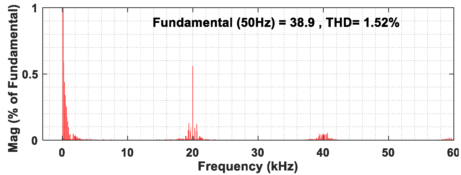
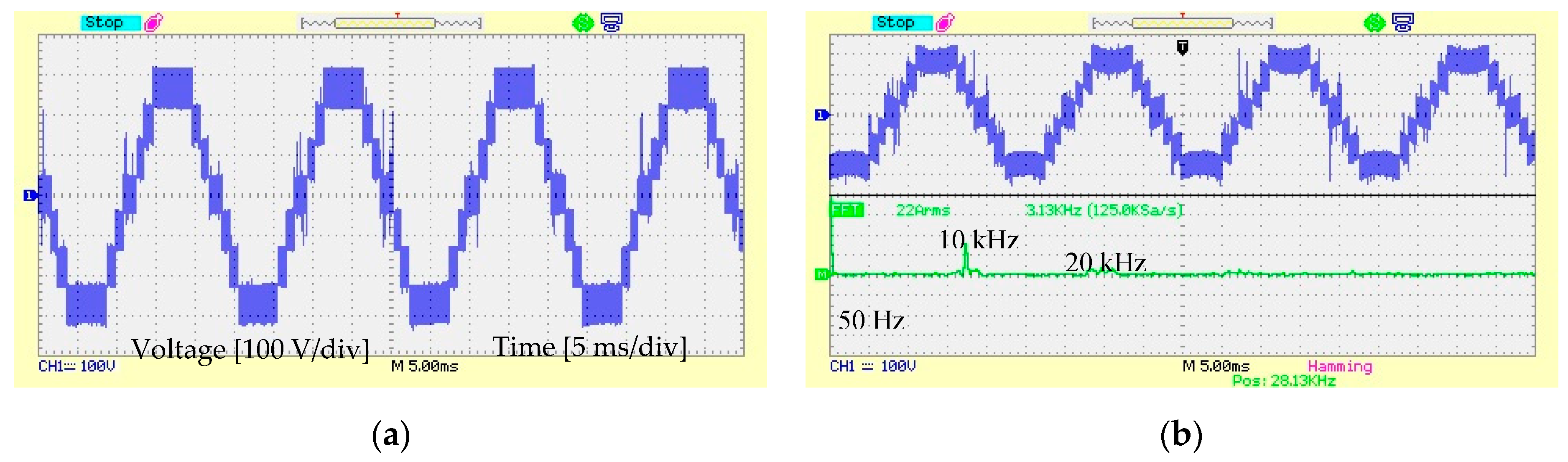
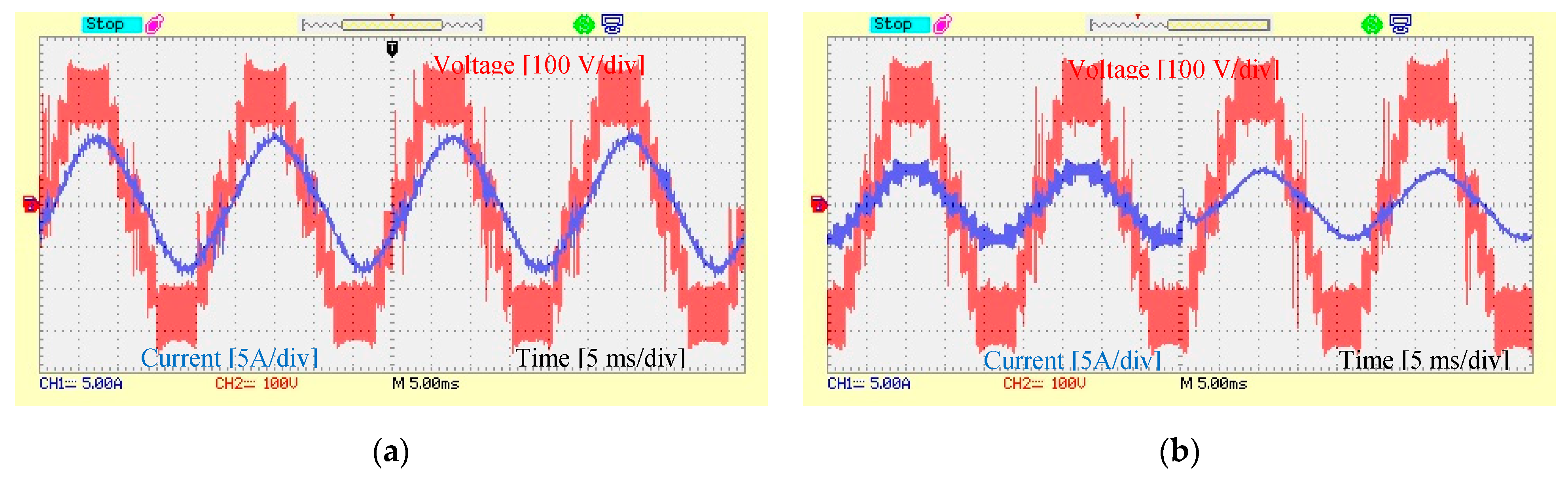
8. Experimental Results

For evaluating the viability of the suggested topology, using a prototype, its performances were investigated under different loading conditions. The characteristics of the prototype are listed in Table 4. The peak value of the output voltage to be developed was considered 320 V and the frequency was 50 Hz. The level-shifted sinusoidal pulse width modulation (SPWM) was used to control power switches. 10 kHz was the switching frequency of the converter. Figure 18 shows the prototype.
Notably, to do FFT analysis, the output voltage should be obtained in the absence of a filter. The developed output voltage under no-load condition is shown in Figure 19a. Meantime, to the end of assessing the quality of the output voltage, the FFT analysis was also illustrated in Figure 19b. Whereas the harmonics mostly appeared around the switching frequency, which can be readily canceled out by virtue of some small filters.
Considering a resistive load of 0.8 kW, the output voltage, input current, and capacitor voltages were scrutinized. The developed output voltage and load current during the abovementioned condition is exhibited in Figure 20a. Moreover, the capacitor voltages are shown in Figure 20b–d. Due to the load current that discharges the capacitors in discharging modes, a voltage ripple appeared on the capacitor voltages. This caused some small ripple on each voltage level, as seen in Figure 20b. Since these voltage ripples were insignificant, they cannot cause a problem.
Inverters are required to supply reactive power upon demand. For investigating the viability of the suggested inverter to supply the reactive power, two scenarios are considered. In the first scenario, the output load was considered 1.2 kVA with lagging PF of 0.94. The output current and voltage at this condition is depicted in Figure 21a. In the second scenario, the dynamic behavior of the inverter was investigated. In this scenario, the prototype was firstly loaded by a resistive load of 0.8 kW, then it was switched to another type of load, which consumed 0.75 kW + 0.28 kVar. The result is illustrated in Figure 21b. The results prove that the proposed inverter can deal with different loading conditions.

9. Conclusions and Future Works

In this study, a SC-based MI for PV applications was suggested. The presented topology is composed of one half-bridge and several basic cells. The leakage current is one of the concerns of PV systems. In addition, the other concern is the low amplitude of the voltage of PV modules. This topology can eradicate the leakage current and provide high-quality boosted ac voltage. In the proposed high step-up MI, the common mode voltage (CMV) oscillates with grid frequency and so does the leakage current, resulting in a mitigated leakage current. The capacitors utilized in the proposed topology are charged spontaneously without any active switch and complicated control approach. Another challenge of modern PV grid-connected systems is their lifetime distribution and identifying the weakest components in a reliability point of view. In this regard, the unreliability curves of the semiconductor devices and the overall system are derived to determine the Bx index. This reliability index showed the worst predicted lifetime of the proposed inverter. The presented lifetime evaluation showed that the switches S1 (or S2) and S5 (or S6) in the proposed inverter have a dominant share in failure. Thus, the proper design of these switches and their cooling system can improve the overall lifetime.
Considering a grid-tied PV system in Matlab/Simulink, the performance of the proposed topology was investigated by assuming various active and reactive powers injecting into the grid. Moreover, the performance of the suggested topology was validated by a laboratory-scaled prototype. The exhibited results in Simulink and experimental results validated the ability of the presented topology to develop high-quality voltage, limiting the leakage current and providing reactive power.
For future work, it is recommended to assess the performance of the proposed inverter under grid voltage sags, non-sinusoidal voltage, and grid voltage distortion conditions. Another interesting research topic is to improve the performance of the proposed inverter by optimizing the design and control parameters to increase efficiency and stability under abnormal conditions.

Author Contributions

Equal attempts were made by all authors to complete the final version of this paper. All authors have read and agreed to the published version of the manuscript.

Funding

This research was funded by the knowledge foundation, Mid Sweden University, 85170 Sundsvall, Sweden.

Institutional Review Board Statement

Not applicable.

Informed Consent Statement

Not applicable.

Data Availability Statement

Figure 13 data can be found here: https://re.jrc.ec.europa.eu/pvg_tools/en/#PVP (accessed on 4 March 2021). The Photovoltaic Geographical Information System (PVGIS) is introduced by [28].

Conflicts of Interest

The authors declare that they have no known competing financial interests or personal relationships.

References

  1. Eskandari, R.; Babaei, E.; Sabahi, M.; Ojaghkandi, S.R. Interleaved high step-up zero-voltage zero-current switching boost DC–DC converter. IET Power Electron. 2020, 13, 96–103. [Google Scholar] [CrossRef]
  2. Vazquez, N.; Rosas, M.; Hernandez, C.; Vazquez, E.; Perez-Pinal, F.J. A New Common-Mode Transformerless Photovoltaic Inverter. IEEE Trans. Ind. Electron. 2015, 62, 6381–6391. [Google Scholar] [CrossRef]
  3. Vazquez, N.; Vazquez, J.; Vaquero, J.; Hernandez, C.; Vazquez, E.; Osorio, R. Integrating Two Stages as a Common-Mode Transformerless Photovoltaic Converter. IEEE Trans. Ind. Electron. 2017, 64, 7498–7507. [Google Scholar] [CrossRef]
  4. Xiao, H.; Xie, S.; Chen, Y.; Huang, R. An Optimized Transformerless Photovoltaic Grid-Connected Inverter. IEEE Trans. Ind. Electron. 2011, 58, 1887–1895. [Google Scholar] [CrossRef]
  5. Yu, W.; Lai, J.-S.; Qian, H.; Hutchens, C.; Zhang, J.; Lisi, G.; Djabbari, A.; Smith, G.; Hegarty, T. High-efficiency inverter with H6-type configuration for photovoltaic non-isolated ac module applications. In Proceedings of the 2010 Twenty-Fifth Annual IEEE Applied Power Electronics Conference and Exposition (APEC), Palm Springs, CA, USA, 21–25 February 2010; pp. 1056–1061. [Google Scholar]
  6. Victor, M.; Greizer, F.; Bremicker, S.; Hübler, U. Method of Converting a Direct Current Voltage from a Source of Direct Current Voltage, More Specifically from a Photovoltaic Source of Direct Current Voltage, into a Alternating Current Voltage. U.S. Patent 7,411,802, 12 August 2008. [Google Scholar]
  7. Yang, B.; Li, W.; Gu, Y.; Cui, W.; He, X. Improved Transformerless Inverter With Common-Mode Leakage Current Elimination for a Photovoltaic Grid-Connected Power System. IEEE Trans. Power Electron. 2012, 27, 752–762. [Google Scholar] [CrossRef]
  8. Su, X.; Sun, Y.; Lin, Y. Analysis on Leakage Current in Transformerless Single-Phase PV Inverters Connected to the Grid. In Proceedings of the 2011 Asia-Pacific Power and Energy Engineering Conference, Wuhan, China, 25–28 March 2011; pp. 1–5. [Google Scholar]
  9. Gu, Y.; Li, W.; Zhao, Y.; Yang, B.; Li, C.; He, X. Transformerless Inverter With Virtual DC Bus Concept for Cost-Effective Grid-Connected PV Power Systems. IEEE Trans. Power Electron. 2013, 28, 793–805. [Google Scholar] [CrossRef]
  10. Bruckner, T.; Bernet, S.; Guldner, H. The Active NPC Converter and Its Loss-Balancing Control. IEEE Trans. Ind. Electron. 2005, 52, 855–868. [Google Scholar] [CrossRef]
  11. Xia, Y.; Roy, J.; Ayyanar, R. A Capacitance-Minimized, Doubly Grounded Transformer less Photovoltaic Inverter with Inherent Active-Power Decoupling. IEEE Trans. Power Electron. 2017, 32, 5188–5201. [Google Scholar] [CrossRef]
  12. Eskandari, R.; Jahan, H.K.; Shotorbani, A.M.; Abapour, M.; Peyghami, S.; Blaabjerg, F. Asymmetric Cascaded Multilevel Inverter with Capacitor-based Half-bridge Cells and Reduced Number of Components. In Proceedings of the 2020 IEEE 21st Workshop on Control and Modeling for Power Electronics (COMPEL), Aalborg, Denmark, 9–12 November 2020; pp. 1–6. [Google Scholar]
  13. Bertilson, K.; Alishah, S.R.; Hosseini, H.S.; Babaei, E.; Aalami, M.; Ali, S.M.J.; Gharehpetian, B.G. A new generalized cascade multilevel converter topology and its improved modulation technique. Int. J. Circ. Theor. Appl. 2020. [Google Scholar] [CrossRef]
  14. Alishah, R.S.; Hosseini, S.H.; Babaei, E.; Sabahi, M.; Gharehpetian, G.B. New high step-up multilevel converter topology with self-voltage balancing ability and its optimization analysis. IEEE Trans. Ind. Electron. 2017, 64, 7060–7070. [Google Scholar] [CrossRef]
  15. Falck, J.; Felgemacher, C.; Rojko, A.; Liserre, M.; Zacharias, P. Reliability of Power Electronic Systems: An Industry Perspective. IEEE Ind. Electron. Mag. 2018, 12, 24–35. [Google Scholar] [CrossRef] [Green Version]
  16. Rahimi, T.; Hosseini, S.H.; Sabahi, M.; Gharehpetian, G.B.; Abapour, M. Reliability evaluation of a fault-tolerant three-phase interleaved DC-DC boost converter. Trans. Inst. Meas. Control 2019, 41, 1278–1289. [Google Scholar] [CrossRef]
  17. Flicker, J. PV inverter performance and component-level reliability. Presented at the 2014 NREL PV Module Reliability Workshop (PVMRW), Golden, CO, USA, 25–26 February 2014. [Google Scholar] [CrossRef]
  18. Cupertino, A.F.; Lenz, J.M.; Brito, E.M.S.; Pereira, H.A.; Pinheiro, J.R.; Seleme, S.I. Impact of the mission profile length on lifetime prediction of PV inverters. Microelectron. Reliab. 2019, 100–101, 113427. [Google Scholar] [CrossRef]
  19. Sintamarean, N.-C.; Blaabjerg, F.; Wang, H.; Yang, Y. Real Field Mission Profile Oriented Design of a SiC-Based PV-Inverter Application. IEEE Trans. Ind. Appl. 2014, 50, 4082–4089. [Google Scholar] [CrossRef]
  20. Haji-Esmaeili, M.M.; Naseri, M.; Khoun-Jahan, H.; Abapour, M. Fault-tolerant structure for cascaded H-bridge multilevel inverter and reliability evaluation. IET Power Electron. 2017, 10, 59–70. [Google Scholar] [CrossRef]
  21. Peyghami, S.; Wang, Z.; Blaabjerg, F. A Guideline for Reliability Prediction in Power Electronic Converters. IEEE Trans. Power Electron. 2020, 35, 10958–10968. [Google Scholar] [CrossRef]
  22. Rahimi, T.; Jahan, H.; Blaabjerg, F.; Bahman, A.; Hosseini, S. Fuzzy-Logic-Based Mean Time to Failure (MTTF) Analysis of Interleaved Dc-Dc Converters Equipped with Redundant-Switch Configuration. Appl. Sci. 2018, 9, 88. [Google Scholar] [CrossRef] [Green Version]
  23. Rahimi, T.; Ding, L.; Faraji, R.; Kheshti, M.; Pou, J. Performance Improvement of a Three-Phase Interleaved DC-DC Converter without Requiring Anti-Saturation Control for Post-Fault Conditions. IEEE Trans. Power Electron. 2020. [Google Scholar] [CrossRef]
  24. Sayed, A.; El-Shimy, M.; El-Metwally, M.; Elshahed, M. Reliability, Availability and Maintainability Analysis for Grid-Connected Solar Photovoltaic Systems. Energies 2019, 12, 1213. [Google Scholar] [CrossRef] [Green Version]
  25. Yang, Y.; Sangwongwanich, A.; Blaabjerg, F. Design for Reliability of Power Electronics for Grid-Connected Photovoltaic Systems. CPSS Trans. Power Electron. Appl. 2016, 1, 92–103. [Google Scholar] [CrossRef]
  26. Anurag, A.; Yang, Y.; Blaabjerg, F. Thermal Performance and Reliability Analysis of Single-Phase PV Inverters with Reactive Power Injection Outside Feed-In Operating Hours. IEEE J. Emerg. Sel. Top. Power Electron. 2015, 3, 870–880. [Google Scholar] [CrossRef]
  27. Sangwongwanich, A.; Yang, Y.; Sera, D.; Blaabjerg, F. Mission Profile-Oriented Control for Reliability and Lifetime of Photovoltaic Inverters. IEEE Trans. Ind. Appl. 2020, 56, 601–610. [Google Scholar] [CrossRef] [Green Version]
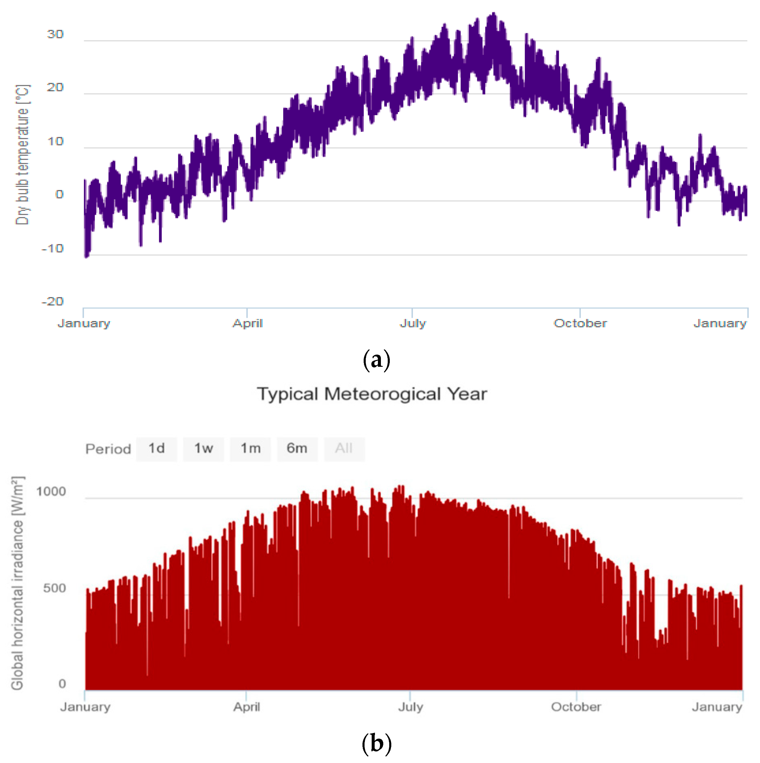
  28. Huld, T.; Müller, R.; Gambardella, A. A new solar radiation database for estimating PV performance in Europe and Africa. Sol. Energy 2012, 86, 1803–1815. [Google Scholar] [CrossRef]
  29. Lee, S. Single-Stage Switched-Capacitor Module (S3CM) Topology for Cascaded Multilevel Inverter. IEEE Trans. Power Electron. 2018, 33, 8204–8207. [Google Scholar] [CrossRef] [Green Version]
  30. Phanikumar, C.; Roy, J.; Agarwal, V. A Hybrid Nine-Level, 1-ϕ Grid Connected Multilevel Inverter with Low Switch Count and Innovative Voltage Regulation Techniques across Auxiliary Capacitor. IEEE Trans. Power Electron. 2019, 34, 2159–2170. [Google Scholar] [CrossRef]
  31. Liu, J.; Lin, W.; Wu, J.; Zeng, J. A Novel Nine-Level Quadruple Boost Inverter with Inductive-Load Ability. IEEE Trans. Power Electron. 2019, 34, 4014–4018. [Google Scholar] [CrossRef]
  32. Sandeep, N.; Yaragatti, U.R. Operation and Control of an Improved Hybrid Nine-Level Inverter. IEEE Trans. Ind. Appl. 2017, 53, 5676–5686. [Google Scholar] [CrossRef]
  33. Radwan, E.; Nour, M.; Awada, E.; Baniyounes, A. Fuzzy Logic Control for Low-Voltage Ride-Through Single-Phase Grid-Connected PV Inverter. Energies 2019, 12, 4796. [Google Scholar] [CrossRef] [Green Version]
  34. Miret, J.; Camacho, A.; Castilla, M.; García de Vicuña, J.L.; de la Hoz, J. Reactive current injection protocol for low-power rating distributed generation sources under voltage sags. IET Power Electron. 2015, 8, 879–886. [Google Scholar] [CrossRef] [Green Version]
  35. Leal, A.C.; Trujillo, C.; Piedrahita, F.S. Comparative of Power Calculation Methods for Single-Phase Systems under Sinusoidal and Non-Sinusoidal Operation. Energies 2020, 13, 4322. [Google Scholar] [CrossRef]
Figure 1. Proposed switched-capacitor (SC)−based multilevel inverter (MI): (a) Basic cell; (b) general configuration.
Energies 14 01915 g001
Figure 2. Eight−level configuration of the proposed topology.
Energies 14 01915 g002
Figure 3. Switching patterns to develop different voltage levels: (a) 3.5 Vdc; (b) 2.5 Vdc; (c) 1.5 Vdc; (d) 0.5 Vdc; (e) −0.5 Vdc; (f) −1.5 Vdc; (g) −2.5 Vdc; (h) −3.5 Vdc.
Energies 14 01915 g003
Figure 4. Stray capacitor in the proposed topology.
Energies 14 01915 g004
Figure 5. Proposed topology integrated with a front−end boost converter.
Energies 14 01915 g005
Figure 6. Control diagram of the proposed inverter in grid-tied photovoltaic (PV) system.
Energies 14 01915 g006
Figure 7. Active and reactive power provided in grid−tied mode.
Energies 14 01915 g007
Figure 8. Output voltage of the inverter and the grid−side current.
Energies 14 01915 g008
Figure 9. Fast Fourier transform (FFT) analysis of the grid current.
Energies 14 01915 g009
Figure 10. Leakage current in grid−tied mode.
Energies 14 01915 g010
Figure 11. Active and reactive power variations of the three−phase configuration.
Energies 14 01915 g011
Figure 12. Voltage and current in grid−tied mode of the three-phase structure: (a) Voltage waveforms of the inverter output; (b) injected current.
Energies 14 01915 g012
Figure 13. Yearly mission profiles in north of Lake Urmia: (a) Solar irradiance level; (b) ambient temperature.
Energies 14 01915 g013
Figure 14. Junction temperatures of: (a) Switches (S1 to S6); (b) diodes (D1 to D4) in grid−connected PV inverter under the yearly mission profile.
Energies 14 01915 g014
Figure 15. Lifetime profile derivation process for the proposed PV inverter with the reliability block diagrams.
Energies 14 01915 g015
Figure 16. Unreliability results from the Monte Carlo simulation: (ac) Switches (S1 to S6); (d) power diodes (d1 to d4).
Energies 14 01915 g016
Figure 17. System level unreliability curve.
Energies 14 01915 g017
Figure 18. Eight-level laboratory-scaled prototype.
Energies 14 01915 g018
Figure 19. Performance of the proposed inverter: (a) Output voltage under no-load conditions; (b) FFT analysis of the voltage signal.
Energies 14 01915 g019
Figure 20. Performance of the inverter while feeding purely resistive load: (a) Load-side voltage and output current of the inverter (bd) voltages of the capacitor in the first, second, and third cells, respectively.
Energies 14 01915 g020
Figure 21. Performance under different loading conditions: (a) Output voltage and load current under resistive-inductive load; (b) output voltage and load current under dynamic loading condition.
Energies 14 01915 g021
Table 1. Operational states of the inverter.
LevelSwitches
States
Diodes
States
Capacitors
States
Vout
S1,S2,S3,S4,S5,S6d1,d2,d3,d4Cu2, Cl2, Cu3, Cl4
41010100101D, C, D, C3.5 Vdc
30110101001C, F, D, C2.5 Vdc
21001100110F, C, C, F1.5 Vdc
10101101010C, N, C, F0.5 Vdc
−11010010101N, C, F, C−0.5 Vdc
−20110011001C, F, F, C−1.5 Vdc
−31001010110F, C, C, D−2.5 Vdc
−40101011010C, D, C, D−3.5 Vdc
Table 2. Characteristics of the grid-tied model.
ParametersValues
Input voltage135 V
Cu1,Cl1,Cu2,Cl2,Cu3,Cl32200 µF
Switching strategyLs-SPWM
Grid voltage & frequency20 kHz
Base apparent power6.5 kVA
Base voltage (peak)320 V
L (grid voltage)1.7 mH
Number of cells2
Table 3. Comparison.
TopologyNswitchNdiodeNcapacitorGVTStand_voltageLeakage Current Limiting Capability
[29]12-225.5no
[30]10-20.58yes
[31]83345.75no
[32]12-345.25no
[Proposed]6463.54.86yes
Table 4. Components utilized in the prototype.
ComponentsType
SwitchesIRFP450
Opto-couplerTLP250
MicroprocessorDSP-F28335
Capacitors3300 µF
Switching power supplyiS0515s
DiodesFFPF20UP40S
Publisher’s Note: MDPI stays neutral with regard to jurisdictional claims in published maps and institutional affiliations.

