Article

AC–DC Flyback Dimmable LED Driver with Low-Frequency Current Ripple Reduced and Power Dissipation in BJT Linearly Proportional to LED Current

1
Department of Ph.D. Program, Prospective Technology of Electrical Engineering and Computer Science, and Department of Electrical Engineering, National Chin-Yi University of Technology, No.57, Section 2, Zhongshan Rd., Taiping District, Taichung 41170, Taiwan
2
Department of Electrical Engineering, National Taipei University of Technology, 1, Section 3, Zhongxiao E. Rd., Taipei 10608, Taiwan
3
Chicony Power Technology Co., Ltd., Sanchong, New Taipei City 24158, Taiwan
*
Author to whom correspondence should be addressed.
Energies 2020, 13(16), 4270; https://doi.org/10.3390/en13164270
Submission received: 15 May 2020 / Revised: 12 August 2020 / Accepted: 17 August 2020 / Published: 18 August 2020

Abstract

:
In this paper, a dimmable light-emitting diode (LED) driver, along with the low-frequency current ripple decreased and the bipolar junction transistor (BJT) power dissipation reduced, is developed. This driver is designed based on a single-stage flyback converter. On the one hand, the low-frequency output current ripple reduction is based on the physical behavior of the linear current regulator. On the other hand, when the voltage across the LED string is decreased/increased due to dimming or temperature, the output voltage of the flyback converter will be automatically regulated down/up, thereby making the power dissipation in the BJT linearly proportional to the LED current. By doing so, not only the power loss in the linear current regulator will be decreased as the LED current is decreased or the LED temperature rises, but also the output current ripple can be reduced. Furthermore, the corresponding power factor (PF) is almost not changed, and the total harmonic distortion (THD) is improved slightly. In addition, the LED dimming is based on voltage division. Eventually, a 30 W LED driver, with an input voltage range from 85 to 295 Vrms and with 24 LEDs in series used as a load, is developed, and accordingly, the feasibility of the proposed LED driver is validated by experimental results.

Graphical Abstract

1. Introduction

As generally recognized, the light-emitting diode (LED) is becoming more attractive in the world due to its small size, light weight, and long life [1,2]. In general, LED drivers with dimming from 100% to 10% are widely used. Adjusting the light level between 10% and 5% is called deep dimming. Modulating the light output through an LED’s current is achieved either by pulse width modulation (PWM) switching, or by amplitude control, also known as analog or level dimming. The former allows deep deeming but presents low luminous efficiency and a risk of flicker [3]. The latter is inherently safer with respect to flicker, but changes the LED operating point and hence the colorimetric characteristics [4]. For those reasons, PWM is the preferred method, and the corresponding dimming frequency is kept above 3.6 kHz to meet flicker specifications.
However, if the DC current with the low-frequency current ripple, due to the mains, is applied to the LED, the flickering will also occur [5]. Consequently, how to reduce this ripple is a very important issue. The flickering will make the human body uncomfortable and the human eye tired [6]. On the other hand, As well known, the LED lighting is an energy-saving device. Therefore, if the LED lighting can be dimmable, more energy will be savedm and the corresponding additional cost will be decreased. As well recognized in industrial applications, the DC LED driver can be classified into three types. One is the single-stage constructed by the flyback converter [7], another is the two-stage built up by the flyback and buck converters [8], and the other is the two-stage established by the boost and flyback/forward converters [9]. The first type has a simple structure, low cost, and high efficiency, but with a high low-frequency current ripple. However, the second and third types are of small low-frequency current ripple, but with complex structure, high cost, and low efficiency. Accordingly, the first type has a more serious flickering problem than the other two.
Therefore, how to reduce LED flickering is a research issue in this paper. The literature [10] presents a comprehensive experimental-based labeling methodology for comparing LED performance with reference to light flicker and power factor. The literature [11] presents an auxiliary circuit with battery powering, and by controlling this circuit, a current opposite to the low-frequency current ripple is generated to suppress such a current ripple. The literatures [12,13] adopt the three-phase voltage along with the power factor correction (PFC) to decrease the low-frequency current ripple. The literature [14,15] employs some auxiliary circuits, which will generate energy via different paths and transfer this energy to the output so that the low-frequency current ripple can be inhibited. The literature [16,17] also utilizes the third-order harmonic injection so that the input power pulsation will be smoothed; hence, the low-frequency current ripple can be alleviated, but the corresponding power factor (PF) is degraded. Furthermore, the literature [18,19] employs the valley-fill circuits, which will change the turn-on angle between the input instantaneous power and the input current, so that the low-frequency current ripple can be reduced. However, the above-mentioned methods have a common default of circuit complexity and design difficulty. Consequently, in this paper, a single-stage AC–DC flyback LED driver, together with a linear current regulator having the bipolar junction transistor (BJT) whose power dissipation is only linearly proportional to the LED current, is employed so as to decrease LED low-frequency flicker significantly with PF and total harmonic distortion (THD) slightly influenced. In addition, amplitude dimming from 100% to 10% is adopted herein.

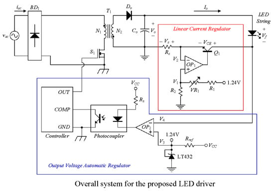
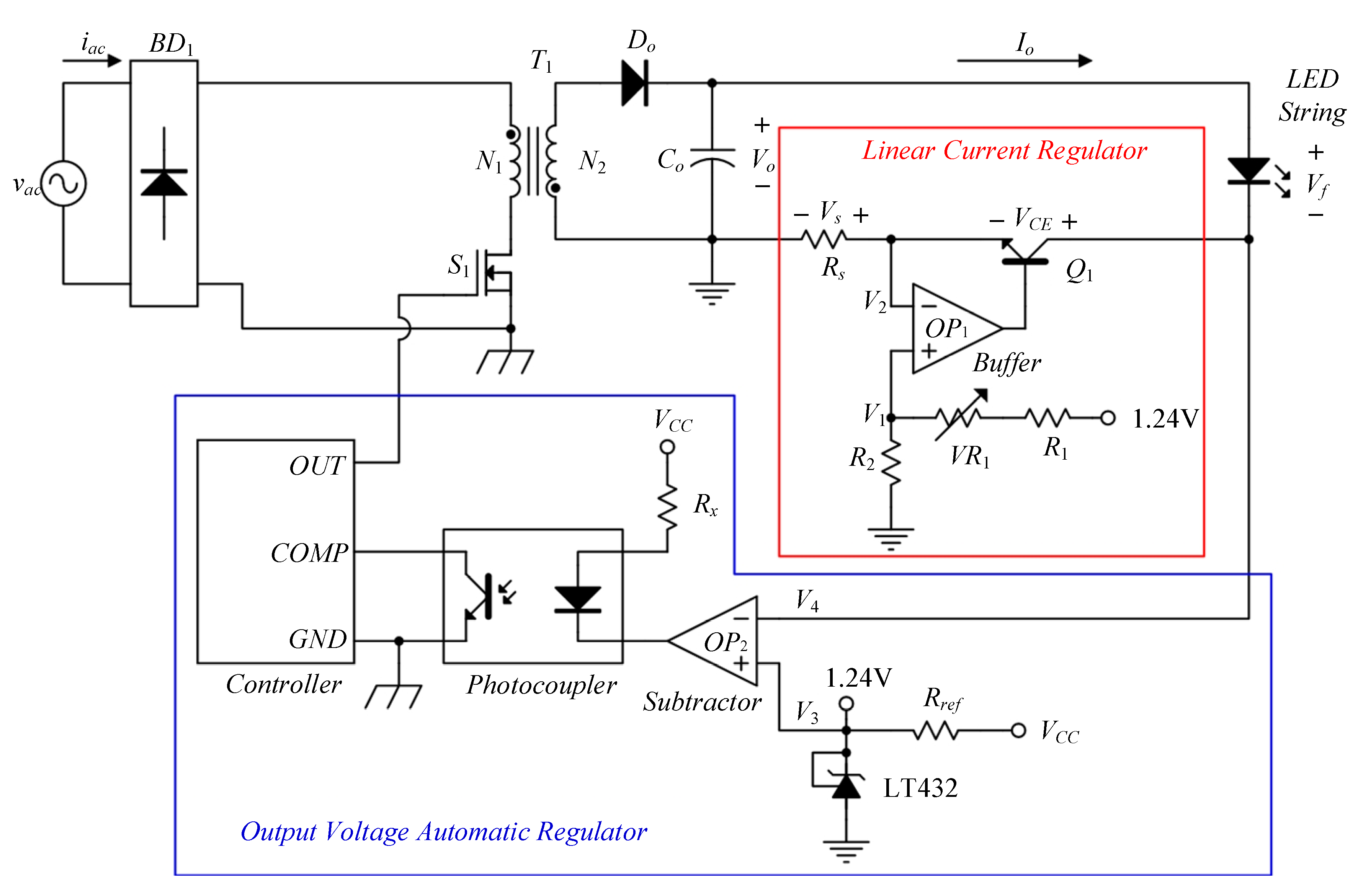
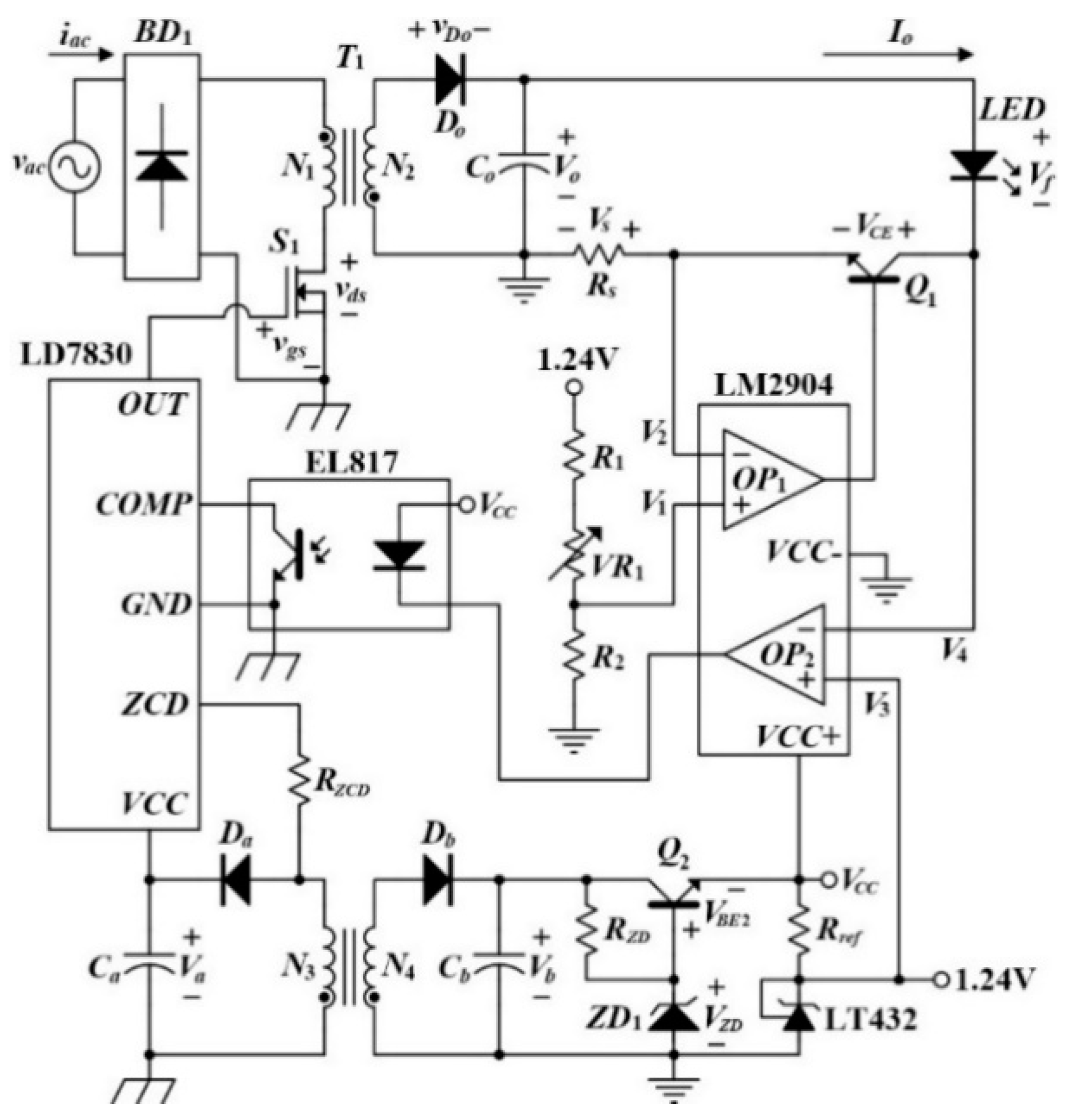
2. Basic Operating Principles of the Proposed Circuit

Figure 1 displays the system block diagram for the proposed LED driver, and Figure 2 briefly illustrates its overall system. Figure 2 shows the proposed circuit with the input voltage vac and the input current iac before the bridge diode BD1. This circuit contains three subsystem blocks. The first subsystem block is the main power stage constructed by one single-stage flyback converter with the transformer T1 having the primary turns of N1 and the secondary turns of N2. The second subsystem block is the linear current regulator along with a dimming function built up by one operational amplifier OP1 used as a buffer with the voltage V1 at the non-inverting input terminal and the voltage V2 at the inverting input terminal, one BJT Q1 operating in the linear region, one current-sensing resistor Rs, and three voltage-dividing resistors R1, R2, and VR1, whose value can be adjustable. The third subsystem block is the output voltage automatic regulator established by one operational amplifier OP2 used as a subtractor with the voltage V3 at the non-inverting input terminal and the sensed voltage V4 at the inverting input terminal, one adjustable precision shunt regulator TL432 providing one reference voltage V3 of 1.24 V via the circuit voltage VCC, one photocoupler, one controller, and two current-limiting resistors Rx and Rref. Furthermore, the voltages Vo, Vf, and Vs indicate that the output voltage of the flyback converter, the equivalent forward voltage of the LED string, and the voltage across Rs, respectively. In addition, the voltage V2 is equal to the voltage V1 based on the virtual ground, and the current Io is the current flowing through the LED string.

3. Basic Operating Concept

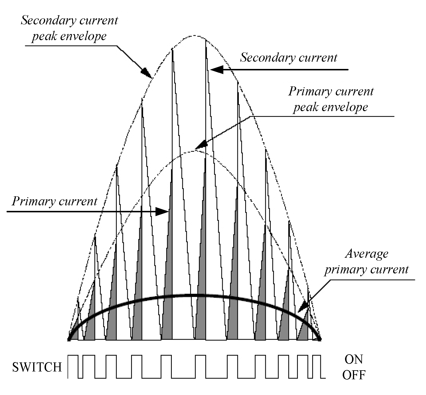
3.1. Reduction of Low-Frequency Output Current Ripple

Figure 1 displays the basic operating concept for reduction of the low-frequency output current ripple. As generally acknowledged, the single-stage flyback converter, operating under voltage control, can be regarded as a voltage source, and the linear current regulator under current control can be viewed as a current source. Therefore, the internal impedance of the linear current regulator is much larger than the equivalent impedance of the LED string. That is, the voltage ripple on the LED string is much lower than that on the linear current regulator based on the voltage division, thereby causing the corresponding current ripple in the LED string to be reduced significantly.

3.2. System Stability Based on Simple Circuit Concept

From the circuit concept point of view, the voltage source can be regarded as a capacitor with an infinite capacitance and vice versa, and the current source can be viewed as an inductor with an infinite inductance and vice versa [20]. Hence, the circuit in Figure 1 can be considered as a series RLC circuit, consisting of a resistor (R), an inductor (L) and a capacitor (C), and the quality factor Q is the characteristic impedance Zo divided by the equivalent resistance of the LED string, called R, where Zo is L / C , which is equal to one based on the limit concept [21]. Hence, the value Q, equal to Z o / R , is quite small since the value of R is larger than one, about 50 Ω in this paper, thereby making the phase margin quite large and guaranteeing that the circuit is stable [22].

3.3. Output Voltage Automatic Regulator

From Figure 1, the relationship between the voltages Vo, Vf, VCE and Vs can be represented by
V o = V f + V C E + V s .
From (1), since the voltage Vs is relatively low, Equation (1) can be rewritten to be
V o V f + V C E .
From (2), under the condition that the voltage Vo is fixed, if the voltage Vf increases, the voltage VCE decreases, whereas if the voltage Vf decreases, the voltage VCE increases. Under a given value of Io with the corresponding value of VCE, the accompanying power dissipation on Q1, called PQ1, can be expressed as
P Q 1 = V C E × I o .
However, under the condition that the voltage Vo and the current Io are fixed, if the number of LEDs in the LED string is decreased or if the LED temperature is increased, then the voltage Vf will be decreased and the voltage VCE will be increased based on (2). Hence, the power dissipation PQ1 will be increased based on (3).
Consequently, from (2), under the condition that the voltage VCE and the current Io are fixed, if the voltage Vf increases, the voltage Vo increases; otherwise, the voltage Vo decreases. This will be achieved based on output voltage automatic regulation so that the voltage VCE can be kept constant almost at the reference voltage V3 for any time. Therefore, under a given value of Io, the accompanying power dissipation can be expressed as
P Q 1 = V 3 × I o .
Therefore, we can see that the result in (4) will not be affected by any value of VCE. Hence, the lower the load current, the less the power dissipation on Q1. That means that if the value of V3 is suitably chosen near the curve knee of the linear region of Q1 or somewhat more, the power dissipation on Q1 will be reduced all over the output load range and the input voltage range.
Regarding the corresponding operating principle for the output voltage automatic regulator, it will be described based on Figure 2 as follows. First, the sensed feedback voltage V4 is sent to the subtractor, and this voltage is subtracted from the reference voltage V3 to yield an error signal. Then, this error signal is passed to the compensator, named COMP, via the photocoupler, to create a desired gate driving signal, which is sent to the switch S1 via OUT. By doing so, the LED driver can operate in the critical conduction mode (CRM) with VCE kept at 1.24 V and hence Vo kept at some variable value, equal to the sum of Vf and 1.24 V, where Vf is a function of the current, temperature, and the number of LEDs. In addition, the CRM pulse width modulation (PWM) control will make the main switch have near-zero voltage switching (NZVS).

3.4. Operating Principle of CRM PWM Control

The waveforms shown in Figure 3 are used to understand the basic operating principle of the CRM PWM control for the single-stage PF flyback converter. From Figure 3, as soon as the zero current at the secondary is from the positive current to zero, the resonance occurs between the primary inductance and the parasitic capacitance of the main switch. Hence, the current at the primary goes to the negative. As soon as such a current goes to zero, the accompanying voltage on the main switch resonates to the minimum value. At this moment, the main switch is turned on with NZVS, and this is achieved by the auxiliary winding. As seen in Figure 3, the voltage on the auxiliary winding is almost the same as that on the main switch except for the amplitude. Therefore, the zero current detection signal, called ZCD, is attained and compared with a fixed threshold voltage inside the CRM PWM integrated circuit (IC); hence, the resulting gate-driving signal vgs is activated.
As for the control loop of the single-stage PF flyback converter based on the L6561 PWM IC [23], it will have a narrow bandwidth (<20 Hz) to maintain control force almost constant over a given line cycle, and this will ensure a high PF. The higher the PF, the larger the inrush current during the turn-on period, and the slower the transient response. Accordingly, the bandwidth will be designed between 10 and 16 Hz. In addition, based on the CRM PWM control, the right-half-plane zero is removed, and only a single left-half-plane pole exists, thereby making the control design relatively easy [22].
The following mathematical derivative is based on CRM with the small value of td negligible, as shown in Figure 3. Since this converter operates in CRM with the bandwidth of the voltage loop far lower than that of the mains, the turn-on period Ton of the gate-driving signal for the main switch is kept constant at some value, as shown in Figure 4. Therefore, Ton can be expressed in terms of Lp, Im and Vm:
T on = L p i m ( ω t ) v ac ( ω t ) = L p I m V m
where Lp is the primary self-inductance, vac is the AC input voltage, im is the current flowing through Lp, ω is the radian frequency of vac, Vm is the maximum value of vac, and Im is the maximum value of im.
In addition, the turn-off period toff of the gate driving signal is instead variable and can be expressed by
t off = L p I m | sin ( ω t ) | n ( V o + V F )
where toff is the time duration between the instant of turning off the main switch and the instant of detecting the current flowing through the diode at the secondary to be zero, n is the turns ratio of the flyback transformer, equal to N1/N2, Vo is the output voltage, and VF is the voltage across the forward-biased diode at the secondary.
Therefore, based on (5) and (6), the variable switching period ts can be represented by
t s = T o n + t o f f = L p I m [ 1 + K v | sin ( ω t ) | ] V m
where K v = V m / V R , V R = n ( V o + V F ) and VR is the voltage reflected from the secondary to the primary.
Hence, the variable switching frequency fs can be expressed as
f s = V m L p I m [ 1 + K v | sin ( ω t ) | ] .
Then, the minimum switching frequency fs,min can be obtained as
f s , min = V m L p I m ( 1 + K v ) .
According to (5) and (7), the resulting duty cycle d varied with the mains can be expressed as
d = T on t s = 1 1 + K v | sin ( ω t ) | .

4. Design Considerations

In the following, the system specifications are given first, and then the design of the magnetizing inductance, output capacitance, dimming control circuit, linear current regulator, and output voltage automatic regulator follow. In the paper, a single LED, belonging to the Edixeon A1 Series, has the rated forward current of 350 mA and the typical forward voltage of 3.4 V. However, the forward voltage adopts 3.6 V due to a tolerance for different dimming current levels. Consequently, if the number of LEDs is chosen to be 24, then the maximum output voltage is 86.4 V plus 1.24 V and the maximum output current is 350 mA. Based on the above-mentioned, the system specifications are shown in Table 1. In addition, the efficiency at the rated load is assumed to 85% and the minimum switching frequency is set at 55 kHz.

4.1. Design of Magnetizing Inductance Lm

The design procedure for Lm of the transformer T1 is based on the application note AN1059 of the L6561 PWM IC [23], which makes the circuit operate in the CRM. In addition, it is assumed that there is no leakage inductance—that is, the coupling coefficient of the transformer is equal to one; hence, Lm is equal to the primary inductance Lp. There are four steps in design of Lm.

4.1.1. Step 1

From Table 1, some parameters will be used in the design, as shown in Table 2.

4.1.2. Step 2

The peak value of the minimum input voltage vpk,min, the peak value of the maximum input voltage vpk,max, and the rated input power Pin,max are calculated as follows:
v p k , m i n = 2 × v a c , m i n = 2 × 85 = 120.21 V
v p k , m a x = 2 × v a c , m a x = 2 × 295 = 417.19 V
P i n , m a x = P o , max / η = 30.24 / 0.85 = 35.58 W .

4.1.3. Step 3

The expressions of the reflected voltage VR, the maximum duty cycle Dmax, and the ratio of vpk,min to VR, called Kv, are shown below:
V R = n × ( V o , max + V F )
D m a x = V R v p k , m i n + V R
K v = v p k , m i n / V R
where VF is generally set at 1 V in the design.
In order to obtain relatively high utilization of the switch, the value of Dmax is set at about 0.45. Accordingly, the value of n is adjusted based on (14) and (15) so that the value of Dmax is close to 0.45. In this case, the value of n is set at 1.1. Therefore, the values of VR, Dmax, and Kv can be figured out to be
V R = n × ( V o , max + V F ) = 1.1 × ( 86.4 + 1 ) = 96.14 V
D m a x = V R v p k , m i n + V R = 96.14 120.21 + 96.14 = 0.444
K v = v p k , m i n / V R = 120.21 / 96.14 = 1.25 .

4.1.4. Step 4

The expressions of F2(Kv), which is a function of Kv, the peak value of the primary self-inductance current Ip,pk, and the primary self-inductance Lp, are shown below:
F 2 ( K v ) = 0.5 + 0.0014 × K v 1 + 0.815 × K v
I p , p k = 2 × P i n , m a x v p k , m i n × F 2 ( K v )
L p = v p k , m i n / [ ( f s , m i n × I p , p k × ( 1 + K v ) ] .
Based on (13) and (19)–(22), the values of F2(Kv), Ip,pk, and Lp can be worked out to be
F 2 ( K v ) = 0.5 + 0.0014 × K v 1 + 0.815 × K v = 0.5 + 0.0014 × 1.25 1 + 0.815 × 1.25 = 0.249
I p , p k = 2 × P i n , m a x v p k , m i n × F 2 ( K v ) = 2 × 35.58 120.21 × 0.249 = 2.382 A
L p = v p k , m i n / [ ( f s , m i n × I p , p k × ( 1 + K v ) ] = 12 0.21 / [ ( 55 k × 2.382 × ( 1 + 1.25 ) ] = 408 μ H .
Since the transformer T1 has the coupling coefficient of one, Lm = Lp = 408 μH. Hence, an RM8 core is chosen for T1 with N1 = 51 turns and N2 = 46 turns.

4.2. Design of Co

According to Table 1, since the low-frequency output voltage ripple will influence the value of Co significantly, this ripple is assumed to be smaller than 4% of the maximum output voltage Vo,max. Accordingly, based on Table 1, the inequality of Co can be obtained to be [24]:
C o I o , max 2 × π × f a c × Δ v o = 0.35 2 × π × 60 × 86.4 × 0.04 = 269 μ F .
Hence, one 390 μF/100 V Rubycon capacitor is chosen as Co.

4.3. Design of Input Filter

A two-order low-pass filter, with one inductor of 3.2 mH and one plastic capacitor of 0.22 μF, is used as an input filter and inserted between the rectifier and the LED driver. Therefore, the corner frequency of this filter is about 6 kHz. In addition, the harmonics for the THD regulations are measured up to the 39th order, equal to 60 Hz × 39 = 2.34 kHz, which is much lower than the corner frequency used. This means that such a filter does affect the THD slightly. Since the value of PF is the product of the displacement factor and the distortion factor, which is a function of THD, this filter does affect the PF slightly, also.

4.4. Components Used

The components used in the circuit is tabulated in Table 3.

4.5. Design of LED Dimming Circuit

From Figure 1, it can be seen that one variable resistor VR1 is used to change the voltage V1 and then the voltage V2 will be varied, so that the output current Io is altered to achieve LED dimming. In the following equation, the formula for Io can be represented by
I o = 1.24 × ( R c 2 R c 1 + R c 2 + V R 1 ) R s
From Table 1, the output current locates between 10% and 100% of the maximum output current, namely, between 0.035 and 0.35 A. With the values of R1 and R2 set at 4.7 kΩ and 0.3 kΩ, respectively, the maximum output current is 0.372 A as the value of VR1 is zero, whereas the minimum output current is 0.018 A as the value of VR1 is 100 kΩ. These two values, covering the dimming current range, are calculated below:
I o , a d j , max = 1.24 × ( R c 2 R c 1 + R c 2 + 0 ) R s = 1.24 × ( 0.3 k 4.7 k + 0.3 k + 0 ) 0.2 = 0.372 A
I o , a d j , min = 1.24 × ( R c 2 R c 1 + R c 2 + 100 k ) R s = 1.24 × ( 0.3 k 4.7 k + 0.3 k + 100 k ) 0.2 = 0.018 A .

4.6. Design of Linear Current Regulator

From Figure 1, the output current is determined by the following equation:
I o = V s R s V 2 R s .
Based on the LM2904 datasheet, it can be seen that the maximum offset of the input pin is 7 mV. This means that the value of V2 should be larger than 7 mV to avoid this IC having an error in action at minimum output current. Hence, the value of V2 is set at 70 mV, thereby causing the value of Rs to be 0.2 Ω (= 0.07 V/0.35 A).

4.7. Design of Output Voltage Automatic Regulator

4.7.1. Design of V3

In design of the linear current regulator, the value of V3 is set at 1.24 V due to a stable voltage of 1.24 V inside the LT432. Hence, we should make sure that the voltage VCE for Q1 is higher than the voltage VCE,sat to guarantee that Q1 operates in the linear region. According to the datasheet for Q1, called 2SD1816, as the current flowing through Q1 is 410 mA, the corresponding voltage VCE is 1 V, which is larger than the VCE,sat voltage of 0.4 V. In this paper, as the current flowing through Q1 is 350 mA, the resulting voltage VCE is 1.17 V (= 1.24 V − 0.35 A × 0.2 Ω), guaranteeing that Q1 operates in the linear region.

4.7.2. Design of Rx and Rref

From Figure 2, the value of VCC is about 12.3 V. According to the industrial experience, the current flowing through Rx is at least 1 mA to make sure that the photocoupler can operate normally. Therefore, the value of Rx is set at 10 kΩ, causing the current in Rx to be 1.09 mA [= (12.3 − 2.4) V/10 kΩ], where 2.4 V is the voltage of the anode of the diode embedded in the photocoupler. On the other hand, the current flowing through Rref is at least 2 mA to make sure that the TL432 can operates normally. Thus, the value of Rref is set at 4.7 kΩ, thereby making the current in Rref be 2.35 mA [= (12.3 − 1.24) V/4.7 kΩ].

5. Experimental Results

5.1. Test Bench for Measurements

The setup used to measure the efficiency will be briefly described. First, as shown in Figure 5, the values of input power, PF, and THD can be obtained from the power meter. Regarding the output power, the output current is read from a current meter, and the output voltage is read from another voltage meter. Therefore, the output power can be attained. Finally, the efficiency is deduced from those two measurements.
As for measured waveforms, they are also obtained by the instruments shown in Figure 5, along with one additional current amplifier, named Tektronix TCPA300, one additional current probe, named Tektronix TCP305, and one additional isolated oscilloscope, named Tektronix TPS2024B.

5.2. Actual System Circuit

Figure 6 shows the actual system circuit of the proposed LED driver, where the primary auxiliary winding N3, the diode Da, the capacitor Ca, and the resistor RZCD are used to obtain the signal ZCD, and the secondary auxiliary winding N4, the diode Db, the capacitor Cb, the transistor Q2, the Zener ZD1, and the resistor RZD are employed to generate the circuit voltage VCC.

5.3. Measured Waveforms

At 110 and 220 V input voltages and 100% output load, some experimental results, without and with the proposed low-frequency current ripple improved, are given to verify the proposed LED driver.
Under 110 V input voltage and 100% output load, Figure 7 displays the input voltage vac and the input current iac, without and with the proposed method, whereas Figure 8 depicts the ripple of Vf, called Δvf, and the ripple of Io, called Δio, without and with the proposed method. Under 220 V input voltage and 100% output load, Figure 9 displays the input voltage vac and the input current iac, without and with the proposed method, whereas Figure 10 depicts the ripple of Vf, called Δvf, and the ripple of Io, called Δio, without and with the proposed method.
Some comments on measured waveforms will be given as follows:
(1)
For both methods, the higher the input voltage, the larger the input current distortion.
(2)
For both methods, any value of the input voltage affects the low-frequency output voltage ripple and current ripple slightly.
(3)
With the low-frequency current ripple improved, not only the output voltage ripple but also the output current ripple is reduced.

5.4. Electrical Data Comparisons

Electrical data curves: In the following, the power factor, harmonic distortion, and output current ripple percentage without and with the low-frequency current ripple improved are discussed as below.

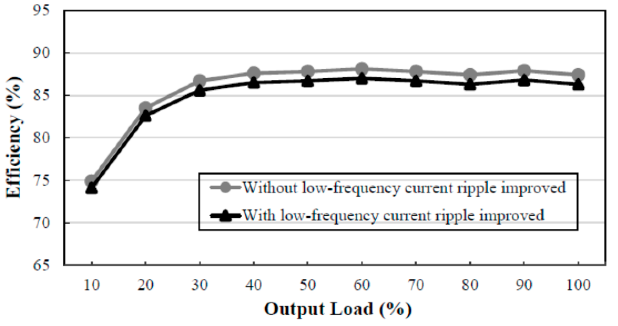
5.4.1. Efficiency Comparison

Efficiency curve: Figure 11 shows curves of efficiency versus output load without and with the low-frequency current ripple improved at the input voltage of 110 V, whereas Figure 12 shows curves of efficiency versus output load without and with the low-frequency current ripple improved at the input voltage of 220 V. From these two figures, the efficiency with a low-frequency current ripple improved is lower than that without a low-frequency current ripple improved by 1.2%. From these two figures, the efficiency at 100% output load with the current ripple improved is 86.3% at the input voltage of 110 V, whereas the efficiency at 100% output load with the low-frequency current ripple improved is 89.2% at the input voltage of 220 V.

5.4.2. Power Factor Comparison

Power factor curve: Figure 13 shows curves of the power factor versus output load without and with the low-frequency current ripple improved at the input voltage of 110 V, whereas Figure 14 shows curves of the power factor versus output load without and with the low-frequency current ripple improved at the input voltage of 220 V. From these two figures, the power factor with the low-frequency current ripple improved is almost the same as that without the low-frequency current ripple improved. From these two figures, the power factor at 50% output load with the low-frequency current ripple improved is 0.994 at the input voltage of 110 V, whereas the power factor at 50% output load with the low-frequency current ripple improved is 0.935 at the input voltage of 220 V.

5.4.3. Total Harmonic Distortion Comparison

Figure 15 shows curves of total harmonic distortion versus output load without and with the low-frequency current ripple improved at the input voltage of 110 V, whereas Figure 16 shows the curves of total harmonic distortion versus output load without and with the low-frequency current ripple improved at the input voltage of 220 V. From these two figures, the total harmonic distortion with the low-frequency current ripple improved is slightly lower than that without the low-frequency current ripple improved. From these two figures, the total harmonic distortion at 50% output load with the low-frequency current ripple improved is 5.6% at the input voltage of 110 V, whereas the total harmonic distortion at 50% output load with the low-frequency current ripple improved is 9.4% at the input voltage of 220 V.

5.4.4. Output Current Ripple Comparison

Figure 17 shows curves of output current ripple versus output load without and with the low-frequency current ripple improved at the input voltage of 110 V, whereas Figure 18 shows curves of output current ripple versus output load without and with the low-frequency current ripple improved at the input voltage of 220 V.
The output current ripple percentage, called Io,ripple%, is defined as
I o , r i p p l e % = ( Δ i o / I o ) × 100 % .
From Figure 17 and Figure 18 and Table 4 and Table 5, it can be seen that with the low-frequency current ripple improved, the output current ripple at 100% output load is lower than that at 10% output load. As compared with the output current ripple percentage without a low-frequency current ripple improved, the output current ripple percentage with the low-frequency current ripple improved can be reduced by a factor of about four at 100% output load and by a factor of about two at 10% output load. From these two figures, the maximum value of the output current ripple percentage with the low-frequency current ripple improved is 4.9%.

6. Comparison

Since the proposed circuit belongs to the step-down circuit, we choose the circuit shown in [5] as a comparison. This circuit is constructed by flyback and buck converters. Since there is no show of THD in [5], the comparison items include the power factor, efficiency, and current ripple percentage. From Table 6, we can see that the proposed converter has better performance than the circuit in [5].

7. Conclusions

In this paper, applying the low-frequency current ripple reduction based on the linear current regulator to the AC-DC flyback LED driver is presented so that LED flickering can be improved. At the same time, adjusting the value of the variable resistor can achieve LED dimming. Furthermore, the output voltage of the flyback converter can be automatically regulated so that the power dissipation in the BJT will be only linearly proportional to the LED current. The results of the comparison between the proposed and the compared are described as following:
(1)
The performance on PF between the two is almost the same.
(2)
The performance on THD between the two is slightly different.
(3)
The maximum difference in efficiency between the compared and the proposed is around 1.2%.
(4)
The maximum difference in output current ripple percentage between the compared and the proposed is around 14%.

Author Contributions

Conceptualization, Y.-T.Y.; methodology, K.-I.H.; software, K.-J.L.; validation, Y.-T.Y.; formal analysis, Y.-T.Y.; investigation, K.-J.L.; resources, K.-I.H.; data curation, K.-J.L.; writing—original draft preparation, K.-I.H.; writing—review and editing, K.-I.H.; visualization, K.-J.L.; supervision, K.-I.H.; project administration, Y.-T.Y.; funding acquisition, K.-I.H. All authors have read and agreed to the published version of the manuscript.

Funding

This research was funded by the Ministry of Science and Technology, Taiwan, under the Grant Number: MOST 108-2221-E-027-051.

Acknowledgments

The authors gratefully acknowledge the support of the Ministry of Science and Technology, Taiwan, under the Grant Number MOST 108-2221-E-027-051.

Conflicts of Interest

The authors declare no conflict of interest.

References

  1. What is LED?-LEDinside. Available online: https://www.ledinside.com.tw/knowledge/20100108-27.html (accessed on 8 January 2018).
  2. ES A1 Series Datasheet—EDISO. Available online: http://www.edison-opto.com.tw/tw/product/es_a1_series (accessed on 12 June 2015).
  3. Loo, K.H. Overview of LED Lighting and Requirements; PE-Workshop, The Hong Kong Polytechnic University: Hong Kong, China, 2011; pp. 1–61. [Google Scholar]
  4. Pousset, N.; Rougie, B.; Razet, A. Impact of current supply on LED colour. Lighting Res. Technol. 2010, 42, 371–383. [Google Scholar] [CrossRef]
  5. Poplawski, M.; Miller, N. SSL Flicker Fundamentals and Why We Care; U.S. Department Energy: Washington, DC, USA, 2014.
  6. U.S. Department of Energy. Solid State Lighting Technology Fact Sheet. Available online: https://www1.eere.energy.gov/buildings/publications/pdfs/ssl/flicker_fact-sheet.pdf (accessed on 1 March 2013).
  7. Wu, S. Single-stage high power factor flyback for LED lighting. Application Note; AN012, RICHTEK. 2014. Available online: http://www.richtek.com/~/media/AN%20PDF/AN012_TW.pdf (accessed on 1 April 2014).
  8. Zhao, S.; Ge, X.; Wu, X.; Zhang, J. Analysis and design considerations of two-stage AC-DC LED driver without electrolytic capacitor. In Proceedings of the 2014 IEEE Energy Conversion Congress and Exposition (ECCE), Pittsburgh, PA, USA, 14–18 September 2014; pp. 2602–2610. [Google Scholar]
  9. Lee, S.; Do, H. Boost-integrated two-switch forward AC-DC LED driver with high power factor and ripple-free output inductor current. IEEE Trans. Ind. Electron. 2017, 64, 5789–5796. [Google Scholar] [CrossRef]
  10. Collin, A.J.; Djokic, S.Z.; Drapela, J.; Langella, R.; Testa, A. Light flicker and power factor labels for comparing LED lamp performance. IEEE Trans. Power Electron. 2019, 55, 7062–7070. [Google Scholar] [CrossRef] [Green Version]
  11. Matsuo, H.; Kurokawa, F.; Lee, B.; Akise, K. Suppression of the input current harmonics and output voltage ripple using the novel multiple-input AC-DC converter. In Proceedings of the 1997 IEEE International Telecommunications Energy Conference (INTELEC), Melbourne, Australia, 23–23 October 1997; pp. 710–714. [Google Scholar]
  12. Hahn, J.; Enjeti, P.N.; Pitel, I.J. A new three-phase power-factor correction (PFC) scheme using two single-phase PFC modules. IEEE Trans. Ind. Appl. 2002, 38, 123–130. [Google Scholar] [CrossRef]
  13. Kamnarn, U.; Chunkag, V. Analysis and design of a modular three-phase AC-to-DC converter using CUK rectifier module with nearly unity power factor and fast dynamic response. IEEE Trans. Power Electron. 2009, 24, 2000–2012. [Google Scholar] [CrossRef]
  14. He, J.; Ruan, X.; Zhang, L. Adaptive voltage control for bidirectional converter in flicker-free electrolytic capacitor-less AC–DC LED driver. IEEE Trans. Ind. Electron. 2017, 64, 320–324. [Google Scholar] [CrossRef]
  15. Qiao, C.; Smedley, K.M. A topology survey of single-stage power factor corrector with a boost type input-current-shaper. IEEE Trans. Power Electron. 2001, 16, 360–368. [Google Scholar] [CrossRef]
  16. Gu, L.; Ruan, X.; Xu, M.; Yao, K. Means of eliminating electrolytic capacitor in AC/DC power supplies for LED lightings. IEEE Trans. Power Electron. 2009, 24, 1399–1408. [Google Scholar] [CrossRef]
  17. Wang, B.; Ruan, X.; Yao, K.; Xu, M. A method of reducing the peak-to-average ratio of LED current for electrolytic capacitor-less AC-DC drivers. IEEE Trans. Power Electron. 2010, 25, 592–601. [Google Scholar] [CrossRef]
  18. Lam, J.C.W.; Jain, P.K. A modified valley fill electronic ballast having a current source resonant inverter with improved line-current total harmonic distortion (THD), high power factor, and low lamp crest factor. IEEE Trans. Ind. Electron. 2008, 55, 1147–1159. [Google Scholar] [CrossRef]
  19. Ma, H.; Lai, J.; Feng, Q.; Yu, W.; Zheng, C.; Zhao, Z. A novel valley-fill SEPIC-derived power supply without electrolytic capacitor for LED lighting application. IEEE Trans. Power Electron. 2012, 27, 3057–3071. [Google Scholar] [CrossRef]
  20. Yau, Y.; Hwu, K.; Jiang, W. Two-phase interleaved boost converter with ZVT turn-on for main switches and ZCS turn-off for auxiliary switches based on one resonant loop. Appl. Sci. 2018, 10, 3881. [Google Scholar] [CrossRef]
  21. Available online: https://math.stackexchange.com/questions/2579556/infinity-divided-by-infinity (accessed on 11 August 2020).
  22. Erickson, R.W. Fundamentals of Power Electronics, 2nd ed.; Kluwer Academic Publishers: Dordrecht, The Netherlands, 2001. [Google Scholar]
  23. Available online: https://www.st.com/resource/en/application_note/cd00004040-design-equations-of-highpowerfactor-flyback-converters-based-on-the-l6561-stmicroelectronics.pdf (accessed on 1 September 2003).
  24. Hwu, K.I.; Yau, Y.T.; Chang, Y.C. Full-digital AC-DC converter with PFC based on counting. IEEE Trans. Ind. Inform. 2015, 11, 122–131. [Google Scholar] [CrossRef]
Figure 1. System block diagram.
Energies 13 04270 g001
Figure 2. Brief illustration of the overall system for the proposed light-emitting diode (LED) driver.
Energies 13 04270 g002
Figure 3. Illustrated waveforms under critical conduction mode (CRM) pulse width modulation (PWM) control.
Energies 13 04270 g003
Figure 4. Current waveforms of the single-stage power factor (PF) flyback converter [23].
Energies 13 04270 g004
Figure 5. Test bench for measuring efficiency, PF, and total harmonic distortion (THD).
Energies 13 04270 g005
Figure 6. Actual system circuit of the proposed LED driver.
Energies 13 04270 g006
Figure 7. Waveforms under 110 V input voltage and 100% output load: (a) without; (b) with the proposed low-frequency current ripple improved: (1) vac; (2) iac.
Energies 13 04270 g007
Figure 8. Waveforms under 110 V input voltage and 100% output load: (a) without; (b) with the proposed low-frequency current ripple improved: (1) Δvf; (2) Δio.
Energies 13 04270 g008
Figure 9. Waveforms under 220 V input voltage and 100% output load: (a) without; (b) with the proposed low-frequency current ripple improved: (1) vac; (2) iac.
Energies 13 04270 g009
Figure 10. Waveforms under 220 V input voltage and 100% output load: (a) without; (b) with the proposed low-frequency current ripple improved: (1) Δvf; (2) Δio.
Energies 13 04270 g010
Figure 11. Curve of efficiency versus output load under 110 V input voltage.
Energies 13 04270 g011
Figure 12. Curve of efficiency versus output load under 220 V input voltage.
Energies 13 04270 g012
Figure 13. Curve of power factor versus output load under 110 V input voltage.
Energies 13 04270 g013
Figure 14. Curve of power factor versus output load under 220 V input voltage.
Energies 13 04270 g014
Figure 15. Curve of total harmonic distortion versus output load under 110 V input voltage.
Energies 13 04270 g015
Figure 16. Curve of total harmonic distortion versus output load under 220 V input voltage.
Energies 13 04270 g016
Figure 17. Curve of output current ripple versus output load under 110 V input voltage.
Energies 13 04270 g017
Figure 18. Curve of output current ripple versus output load under 220 V input voltage.
Energies 13 04270 g018
Table 1. System specifications without the linear current regulator considered.
ParameterSpecification
Input Voltage (vac)90–277 V ± 5% (85–295 V)
Input Voltage Frequency (fac)60 Hz
Maximum Output Voltage (Vo,max)86.4 V ( = 3.6   V   ×   24 )
Maximum Output Current (Io,max)350 mA
Minimum Output Current (Io,min)35 mA
Converter Efficiency ( η )85%
Minimum Switching Frequency (fs,min)55 kHz
LED String24 LEDs in series
Table 2. Design parameters used.
NameSymbolValueUnit
Maximum Output Voltage Vo,max86.4V
Maximum Output CurrentIo,max0.35A
Maximum Output PowerPo,max30.24W
Converter Efficiencyη85%
Minimum Input Voltagevac,min85Vrms
Minimum Input Voltagevac,max295Vrms
Minimum Switching Frequencyfs,min55kHz
Table 3. Component specifications.
ComponentPart Name
S1IPA90R1K2
DoSFF1008G
Co390 uF/100 V Rubycon
T1A-CORE RM8 with N1 = 51, N2 = 46
Q12SD1816
OP1, OP2LM2904
Rs0.2 Ω
R14.7 kΩ
R20.3 kΩ
VR1100 kΩ
Rx10 kΩ
Rref4.7 kΩ
VCC12.3 V
ControllerLD7830
PhotocouplerEL817
Table 4. Measurements of load percentage versus output current ripple percentage at input voltage of 110 V (OCR: output current ripple).
Output Load [%]102030405060708090100
Traditional OCR [%]13.114.314.714.915.116.116.917.617.818.3
Proposed OCR [%]4.94.64.23.93.73.94.24.44.44.6
Improvement Traditional/Proposed2.73.13.53.94.14.14.14.04.04.0
Table 5. Measurements of load percentage versus output current ripple percentage at input voltage of 220 V.
Output Load [%]102030405060708090100
Traditional OCR [%]10.913.013.914.314.615.416.116.516.917.1
Proposed OCR [%]4.94.63.83.43.23.43.63.83.94.0
Improvement Traditional/Proposed2.22.93.74.24.64.54.54.34.44.3
Table 6. Comparison between [5] and the proposed.
Comparison ItemsPower FactorEfficiencyCurrent Ripple Percentage
Input voltage110 V220 V110 V220 V110 V220 V
[5]0.990.9683.8%85.5%<10%<10%
Proposed0.990.9886.3%89.2%<5%<5%

