Abstract
A modified step-down converter is presented herein, which is mainly based on one coupled inductor and several energy-transferring capacitors to improve the voltage conversion ratio as well as to reduce the switch voltage stress. In addition, the portion of the leakage inductance energy can be recycled to the input via the active clamp circuit during the turn-off period and the switches have zero-voltage switching (ZVS) during the turn-on transient. In this paper, the basic operating principles of the proposed converter are firstly described and analyzed, and its effectiveness is finally demonstrated by experiment based on a prototype with input voltage of 60 V, output voltage of 3.3 V and rated output power of 33 W.
1. Introduction
Recently, with the fast development of the servo power and the cloud, the converter with a high step-down voltage conversion ratio is indispensable. However, regarding the traditional buck converter, if a high step-down voltage conversion ratio is required, the corresponding duty cycle is extremely low, thereby causing the control to be difficult, the power loss on the switch to be increased, and the accompanying efficiency to be decreased. Consequently, there are many researches presented to overcome these problems. The literatures [1,2] apply transformers to half-bridge buck converters so as to improve the step-down voltage conversion ratio. The literatures [3,4,5] present switched-capacitor converters, whose step-down voltage conversion ratios are enhanced via capacitor voltage dividers. The literatures [6,7] adopt input voltage dividers along with two transformers to improve step-down voltage conversion ratios as well as to cause voltage stresses on switches to be three-level. The circuits shown in [8,9] are improvements of the circuits shown in [7,10]. The literatures [11,12,13,14,15,16] apply central-tapped coupling inductors to synchronously rectified (SR) buck converters so as to obtain relatively high step-down voltage conversion ratios. In the literatures [17,18,19], via changing the turns ratios of coupling inductors, not only the voltage stresses on switches can be reduced but also relatively high step-down voltage conversion ratios can be achieved. The literature [20] applies a coupling inductor to an SR buck converter so as to improve the step-down voltage conversion ratio. The literatures [21,22,23,24] apply coupling inductors and energy-transferring capacitors to SR buck converters to improve the step-down voltage conversion ratio, and besides, the last employs an active clamp circuit to reduce the switch voltage stress. The circuit shown in [25], with an active clamp circuit included, adopts two forward converters connected in parallel to reduce the voltage conversion ratio. The literature [26] utilizes multiple voltage-bucking modules and energy-transferring capacitors to improve the step-down voltage conversion ratio as well as to reduce the voltage stresses on switches. However, a large number of modules causes the circuit to be complex and the corresponding size to be relatively huge. The literature [27] employs one buck-boost connected in series with two half-bridge DC transformers and three energy-transferring capacitors so as to improve the step-down voltage conversion ratio. As compared with the literature [21], literature [28] utilizes one additional capacitor and one additional inductor so as to obtain more advantages, such as improvement of core size utilization, reduction of output current ripple, etc. In addition, both have the same voltage conversion ratio.
In this paper, a modified step-down converter is presented. As compared with the work [24], the proposed circuit, based on only one additional capacitor inserted and some circuit connections changed, has a relatively wide voltage conversion ratio as well as relatively small voltage stresses on switches. By the way, both have inherent some merits, such as the voltage clamp during the turn-off period, and the zero-voltage switching (ZVS) for switches during the turn-on transient.
2. Circuit Configuration and Its Operating Behavior
Figure 1 shows the proposed converter, which is built up by four switches Q1, Q2, Q3 and Q4, three energy-transferring capacitors C1, C2 and C3, and one coupling inductor with one primary winding N1, one secondary winding N2 and one magnetic inductor Lm. As for the load, it is constructed by one output resistor Ro. Figure 2 displays an equivalent circuit model of the proposed converter.
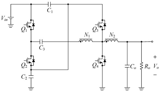
Figure 1.
Proposed improved ultrahigh step-down converter.
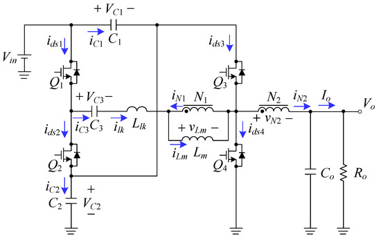
Figure 2.
Equivalent circuit model of the proposed converter.
Prior to tackling this section, there are some associated symbols and assumptions in Figure 2, to be described as follows: (i) the input voltage is Vi; (ii) the output voltage is Vo; (iii) the primary-side and second-side turns are N1 and N2, respectively; (iv) the currents ids1, ids2, ids3, ids4, ic1, ic2, ic3, ilk, iLm, iN1, iN2 and io are the currents in Q1, Q2, Q3, Q4, C1, C2, C3, Llk, Lm, N1, N2 and Ro, respectively; (v) the voltages across Lm, N2, C1, C2, C3 and Co are vLm, vN2, VC1, VC2, VC3 and Vo; (vi) the switching period is signified by Ts; (vii) the turn-on times for Q1 and Q3 are DTs, whereas the turn-on times for Q2 and Q4 are (1 - D)Ts, where D is a duty cycle; (viii) all the switches are ideal, and all the capacitors are ideal without their equivalent series resistances (ESRs) included, that is, the capacitance for each capacitor is assumed to be large enough to keep the voltage on it constant at some value; (ix) the gate driving signals vgs1 and vgs3, for Q1 and Q3 respectively, are identical, whereas the gate driving signals vgs2 and vgs4, for Q2 and Q4 respectively, are identical; and (x) the circuit operates with no negative current. There are six states over one switching period, to be shown in Figure 3.
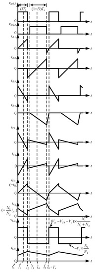
Figure 3.
Key waveforms relevant to the proposed converter operating.
2.1. Operating Principles
2.1.1. State 1: [t0 ≤ t ≤ t1]
As shown in Figure 4, the switches Q1 and Q3 are in the on-state but the switches Q2 and Q4 are in the off-state. The switch Q1 is turned on with zero-voltage switching (ZVS) because the body diode of Q1 is switched on before turn-on of Q1. During this state, the voltages across the magnetizing inductance Lm and leakage inductance Llk are positive voltages, thereby causing Lm and Llk to be magnetized. At the same time, the voltage Vin charges the capacitors C1 and C3, and, together with the capacitor C2, supplies energy to the load. To speak lucidly, at t = t0, the current in C1 has some positive value and then linearly decreases due to the leakage reflected from the primary-side leakage; at t = t0, the current in C2 has some negative value and then linearly decreases due to the leakage reflected from the primary-side leakage; At t = t0, the current in C3 is zero and then linearly increases due to the primary-side leakage. As soon as iC1 and iC2 reach zero, this mode ends at t = t1.
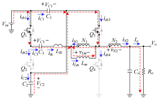
Figure 4.
Current flow during state 1.
2.1.2. State 2: [t1 ≤ t ≤ t2]
As shown in Figure 5, the switches Q1 and Q3 are still in the on-state, but the switches Q2 and Q4 are still in the off-state. During this state, the magnetizing inductance Lm and leakage inductance Llk are still magnetized. At the same time, the input voltage Vin charges the capacitor C2 and, together with the capacitor C1, charges the capacitor C3 as well as supplies energy to the load. Once Q1 is turned off, this mode ends at t = t2.
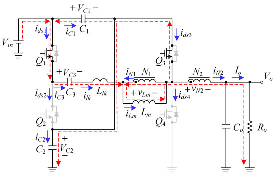
Figure 5.
Current flow during state 2.
2.1.3. State 3: [t2 ≤ t ≤ t3]
As shown in Figure 6, all the switches are turned off with the body diode of Q2 turned on, and this state is called one blanking time over one switching period. During such a state, the voltages across the magnetizing inductance Lm and leakage inductance Llk are negative voltages, thereby causing Lm and Llk to be demagnetized as well as to transfer their energy to the load. At the same time, the capacitor C1 is charged by the input voltage Vin, and the capacitor C2 discharges and, together with Vin, charges the capacitor C3 as well as supplies energy to the load. The moment Q2 and Q4 is turned on, this mode ends at t = t3.
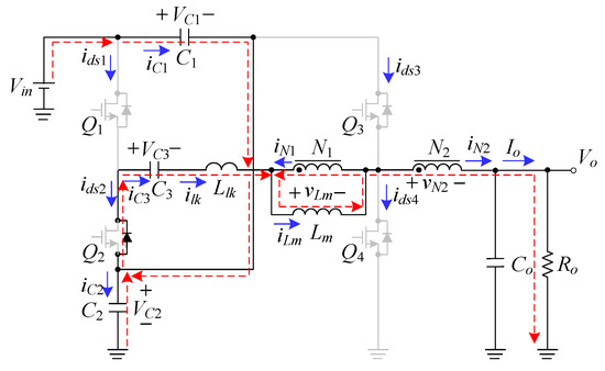
Figure 6.
Current flow during state 3.
2.1.4. State 4: [t3 ≤ t ≤ t4]
As shown in Figure 7, the switches Q2 and Q4 are turned on but the switches Q1 and Q3 are still in the off-state. The switch Q2 is turned on with ZVS because the body diode of Q2 is switched on before turn-on of Q2. During this state, the magnetizing inductance Lm and leakage inductance Llk are still demagnetized, transferring their energy to the load. At the same time, the capacitor C1 is charged by the input voltage Vin, and the capacitor C2 still discharges and, together with the input voltage Vin, still charges the capacitor C3 as well as still supplies energy to the load. As soon as ids2 reaches zero, this mode ends at t = t4.
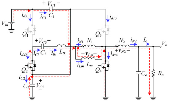
Figure 7.
Current flow during state 4.
2.1.5. State 5: [t4 ≤ t ≤ t5]
As shown in Figure 8, the switches Q2 and Q4 are still in the on-state but the switches Q1 and Q3 are still in the off-state. During this state, the magnetizing inductance Lm and leakage inductance Llk are still demagnetized, transferring their energy to the load. At the same time, the capacitor C3 charges the capacitor C2 and, together with the capacitor C1, releases energy to the input voltage Vin. Once Q2 and Q4 are turned off, this mode ends at t = t5.
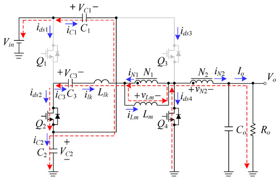
Figure 8.
Current flow during state 5.
2.1.6. State 6: [t5 ≤ t ≤ t0 + Ts]
As shown in Figure 9, all the switches are turned off with the body diodes of Q1 and Q4 turned on and this state is called the other blanking time over one switching period. During such a state, the capacitor C3 still discharges. At the same time, the magnetizing inductance Lm and leakage inductance Llk are still demagnetized, transferring their energy to the load. The moment Q1 and Q3 are turned on, this mode ends and the next cycle is repeated.
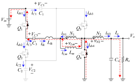
Figure 9.
Current flow during state 6.
2.2. Voltage Conversion Ratio
In order to obtain the voltage conversion ratio, the voltages across the magnetizing inductance Lm, the secondary winding N2, and the energy-transferring capacitors C1, C2 and C3, that is, vLm, vN2, VC1, VC2 and VC3, are first obtained. In the following analysis, the blocking times and the leakage inductance are negligible, and hence only states 1 and 4 are considered. From state 1, the voltages vLm and vN2 can be expressed as
From state 4, the voltages vLm and vN2 can be represented by
Since the magnetizing inductance Lm on the primary side can be reflected to the secondary side, the voltage-second balance should be obeyed over one switching period. Therefore, the following equation can be obtained to be
From (5), we can obtain
Substituting (6) into (3) yields
In addition, since the magnetizing inductance Lm on the primary side also needs to obey the voltage-second balance, the following equation can be obtained to be
By substituting (7) into (8), the voltage conversion ratio can be obtained to be
where n is the turns ratio equal to N2/N1.
2.3. Boundary Condition Analysis
The boundary condition for Lm is described as follows.
where ILm and are the DC and AC values of iLm, respectively, and the latter is also called the magnetizing current ripple.
For analysis convenience, it is assumed that there is no power consumption in the converter. According to the voltage-second balance of the inductor and the current second balance of the capacitor, the DC voltage across the coupling inductor and the DC current in the energy-transferring capacitor are zero. Therefore, as shown in Figure 10, the secondary DC current IN2 is equal to the output current Io, namely,
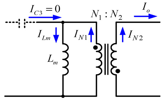
Figure 10.
Equivalent model for the coupling inductor under DC analysis.
From (12) and (13), it can be obtained
Since the current ripple can be expressed as
Hence, as , the magnetizing inductance Lm will be operated without negative current, that is,
where and .
From (16), it can be seen that as K ≥ Kcrit(D), the magnetizing inductance Lm will be operated without negative current; otherwise, Lm will be operated with negative current. Hence, by assuming that N1/N2 = 3, the boundary curve for Lm operating mode can be drawn as shown in Figure 11.
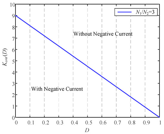
Figure 11.
Boundary curve for Lm operating mode.
2.4. Comparison of Proposed Circuit with Existing Circuits
Table 1 shows the comparison of the proposed circuit with the existing circuits, in terms of voltage conversion ratio, component number, switch voltage stress, and output inductor. From Table 1, the proposed circuit has a more component number than the circuits shown in [24,28] have. As shown in Figure 12, the proposed circuit has a lower voltage conversion ratio than the circuits shown in [24,28] have. In practice, the lower the turns ratio n (= N2/N1) is, the larger the leakage inductance. Consequently, the value of n, set at 1/3 for the comparison in step-down voltage conversion ratio, is reasonable. The proposed circuit has lower voltage stresses on Q1 and Q2 than the circuits shown in [24,28] have. In addition, the proposed circuit has lower voltage stresses on Q3 and Q4 than the circuits shown in [24,28] have. In addition, only the circuit shown in [28] has an output inductor.

Table 1.
Comparison of the proposed circuit with the existing circuits.
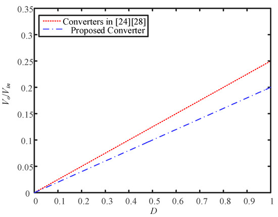
Figure 12.
Voltage conversion curves of the circuit shown in Table 1 with n = 1/3.
3. Control Strategy
Figure 13 shows the system block diagram for the proposed high step-down converter, including main power stage and feedback control circuit. As for the feedback control circuit, it is constructed by one voltage divider used to obtain the analogue signal of the output voltage, one analogue-to-digital converter (ADC) used to transfer this analogue signal to the digital signal, and one field-programmable gate array (FPGA) chip used to generate four digital pulse-width modulation (DPWM) signals, which are sent to four switches after four gate drivers so as to stabilize the output voltage at the desired value. Speaking lucidly, the digital signal obtained from the ADC is sent to the proportional-integral (PI) controller embedded in the FPGA to create DPWM signals, vgs1, vgs2, vgs3 and vgs4, where vgs1 equal to vgs2 is complimentary to vgs2 equal to vgs4.
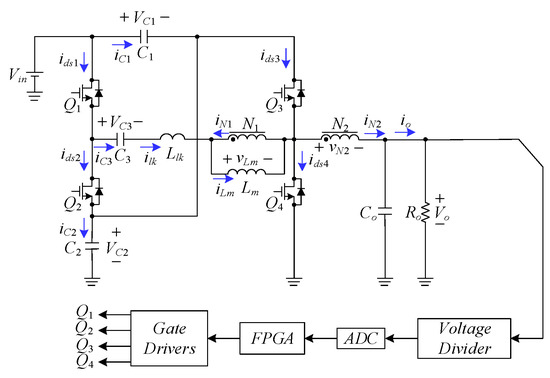
Figure 13.
System configuration block diagram.
How to Set Switching Frequency from FPGA and How to Get DPWM Signal
The FPGA needs an external oscillator of 20 MHz, and this frequency will be increased to 100 MHz, which will be used as a system clock as well as a subsystem clock of the DPWM generator. As soon as the system get started, the counting value of one counter will be increased from zero to 999, and then be initialized such that the next cycle is to be repeated. That is to say, the switching frequency is 100 MHz divided by 1000, equal to 100 kHz. As the counting value of the counter is smaller than the control force created from the PI controller embedded in the FPGA, the DPWM signal will be “high”; otherwise, the DPWM signal will be “low”.
4. Design Considerations
Prior to this section, system specifications should be given as shown in Table 2. The two blanking times between Q1 (or Q3) and Q2 (or Q4) are set at 100 ns and 150 ns, respectively. It is noted that in order to verify that the voltage conversion ratio of the proposed circuit is wider than that of the circuit shown in [24], the former has an input voltage of 60 V and an output voltage of 3.3 V, whereas the latter has an input voltage of 48 V and an output voltage of 3.3 V.
Table 2.
System specifications.
4.1. Design of Coupling Inductor
4.1.1. Design of Turns Ratio
From (9), the following equation can be obtained to be
Since the converter mainly transfers energy to the load during the turn-off period of Q1, the duty cycle is set between 0.2 and 0.3. According to Table 2, together with this desired duty cycle range, the turns ratio inequality can be obtained to be
Based on (18), the value of n is chosen to be
Substituting (19) and some system specifications shown in Table 2 into (19) yields
4.1.2. Design of Magnetizing Inductance
From (16), it can be seen that if the magnetizing inductance Lm operates without negative current, the value of Lm should obey the following inequality:
where Ro,max indicates the maximum output resistance.
Substituting the results shown in (19) and (20), and some specifications shown in Table 2 into (21) yields
Before calculating the primary and secondary turns of the coupled inductor, N1 and N2, the peak current of the magnetizing inductance, ILm,peak, should be first obtained, namely,
By substituting (14) and (15) into (23), the following equation can be obtained to be
By substituting the results shown in (19) and (20), and some specifications shown in Table 2 into (30), the value of ILm,pesak can be obtained to be
After this, via the Faraday law, the value of N1 can be represented by
where Ae is the effective area of the core size and Bmax is the maximum flux density.
Since the saturation flux density Bs will be reduced due to the temperature rising, the value of Bmax is designed to be 80% of Bs. By the way, the high-μ core is used herein, whose product name is PQ20/16-3C90, made by FERROXCUBE Co. Table 3 shows the specifications of this core.
Table 3.
Core specifications.
By substituting the results shown in (22) and (25), and some specifications shown in Table 3 into (26), the value of N1 can be obtained to be
Since the value of n is 1/3, the value of N2 is set at four turns. However, by substituting the result of (27) and the value of Ae shown in Table 3 into the following equation, the corresponding value of Lm, much larger than the value of Lmin shown in (22), can be obtained to be
Consequently, the air gap needs to be adjusted in order to obtain the desired value of Lm. Without considering the fringing effect, the desired value of the airgap lg can be obtained according to the following two equations:
where μe is the equivalent magnetic permeability.
Combining (29) and (30) yields
By substituting the result shown in (22) and some specifications shown in Table 3 into (31), the required value of la can be obtained to be
Finally, the actual value of Lm is designed and measured to be 81.6 μH.
4.2. Component Specifications
In the following, the specifications of the used components are listed in Table 4.
Table 4.
Specifications of the components used in the proposed converter.
5. Experimental Results
5.1. Test Bench for Measuring Efficiency and Waveforms
In the following, how to measure the efficiency will be described. First, as shown in Figure 14, the input current is obtained by measuring the voltage across one current sensing resistor based on one digital meter. After this, the input voltage is obtained also by another digital meter. Hence, the input power can be attained. Regarding the output power, the output current is read from one electronic load and the output voltage is obtained also by the other digital meter. Therefore, the output power can be attained. Finally, the corresponding efficiency can be obtained. As for measured waveforms, they are obtained by the instruments shown in Figure 14, along with two additional current amplifiers, two additional current probes and one additional isolated oscilloscope.
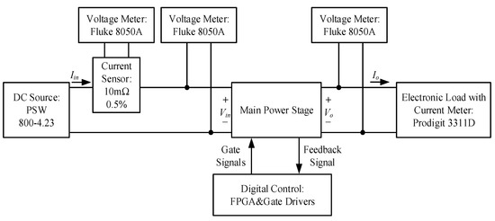
Figure 14.
Test bench for measuring efficiency.
5.2. Measured Waveforms and Efficiency
The waveforms shown in Figure 15, Figure 16, Figure 17, Figure 18, Figure 19, Figure 20 and Figure 21 are measured at rated load. Figure 15 shows the gate driving signal for Q1, vgs1, the voltage across Q1, vds1, the gate driving signal for Q3, vgs3, and the voltage across Q3, vds3. Figure 16 shows the gate driving signal for Q2, vgs2, the voltage across Q2, vds2, the gate driving signal for Q4, vgs4, and the voltage across Q4, vds4. Figure 17 shows the voltages on C1, VC1, the voltage on C2, VC2, and the voltage on C3, VC3. Figure 18 shows the gate driving signal for Q1, vgs1, the gate driving signal for Q2, vgs2, the current flowing through Llk, ilk, and the current in N2, iN2. Figure 19 shows the input voltage Vin and the output voltage Vo. Figure 20 and Figure 21 show the turn-on ZVS of Q1 and Q2, respectively. Figure 22 shows load transient responses and Figure 23 displays a curve of efficiency versus load current percentage.
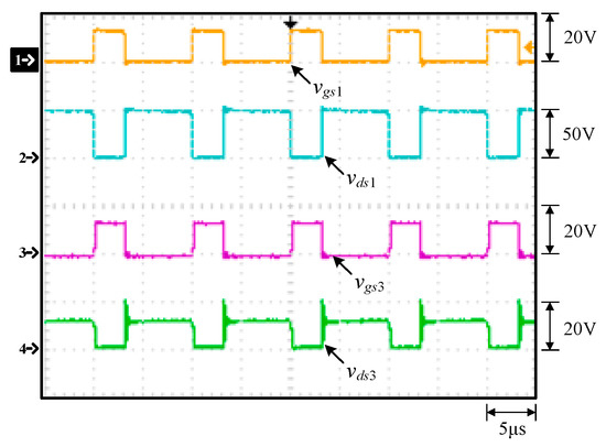
Figure 15.
Measured waveforms at rated load: (1) vgs1; (2) vds1; (3) vgs3; (4) vds3.
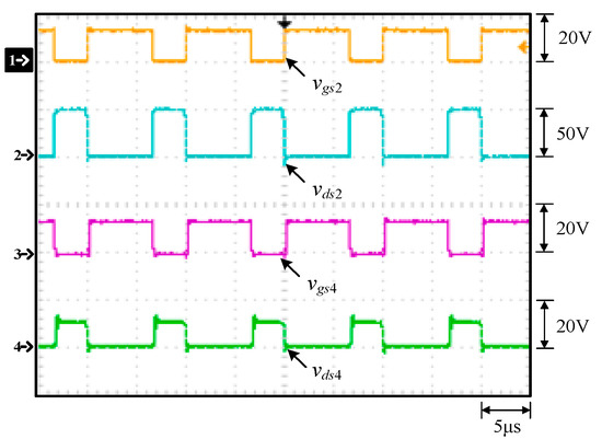
Figure 16.
Measured waveforms at rated load: (1) vgs2; (2) vds2; (3) vgs4; (4) vds4.
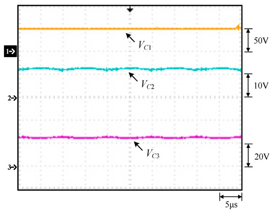
Figure 17.
Measured waveforms at rated load: (1) VC1; (2) VC2; (3) VC3.
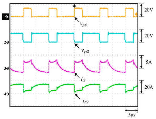
Figure 18.
Measured waveforms at rated load: (1) vgs1; (2) vgs2; (3) ilk; (4) iN2.
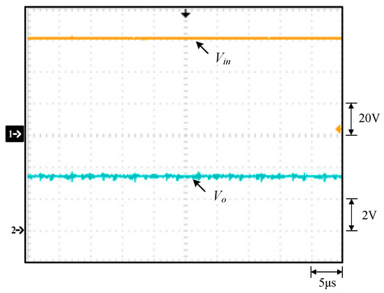
Figure 19.
Measured waveforms at rated load: (1) Vin; (2) Vo.
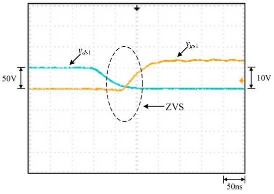
Figure 20.
Zoom-in of the turn-on transient of Q1.
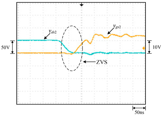
Figure 21.
Zoom-in of the turn-on transient of Q2.
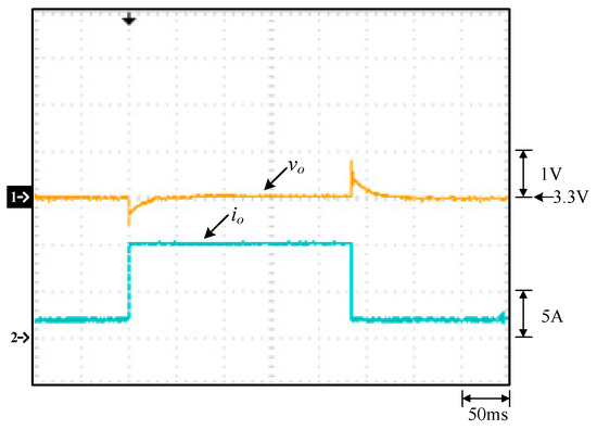
Figure 22.
Output voltage responses due to load transients from light/rated load to rated/light load.
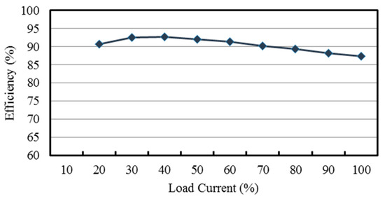
Figure 23.
Curve of efficiency versus load current percentage.
From Figure 15, it can be seen that the voltage stress across Q1 is 48 V, equal to Vin minus VC2 (= 60 V − 12 V), whereas it can be seen that the voltage stress across Q3 is 12 V, equal to Vin minus VC1 (= 60 V − 48 V) with the voltage spike on Q3 due to the parasitic capacitance of the switch resonating with the line parasitic inductance and the leakage inductance of the coupling inductor. From Figure 16, it can be seen that the voltage stress across Q2 is 48 V, equal to Vin minus VC2 (= 60 V − 12 V), whereas it can be seen that the voltage stress across Q4 is 12 V, equal to Vin minus VC1 (= 60 V − 48 V). From Figure 17, the voltages on C1, C2 and C3, namely, VC1, VC2 and VC3, are almost kept constant at some values. From Figure 18, it can be seen that there are some differences in ilk and iN2 between the waveforms shown in Figure 4 and these measured waveforms. This is because the leakage inductance of the coupled inductor will resonate with the energy-transferring capacitors. From Figure 19, it can be seen that the output voltage can be stably kept at 3.3 V under the input voltage of 60 V. From Figure 20 and Figure 21, it can be seen that the switches Q1 and Q2 have ZVS turn-on since these two switches are switched on after individual body diodes are turned on, corresponding to states 1 and 4 in Section 2. Figure 22 shows the load transient response from light load to rated load with a undershoot of 600 mV and a recovery time of 30 ms, and the load transient response from rated to light load with an overshoot of 800 mV and a recovery time of 55ms. Figure 23 shows that the overall efficiency is above 87.4% and can be up to 92.7%.
6. Conclusions
The proposed step-down converter comes from the converter [28]. Although the former, with one additional capacitor, has larger number of components than the latter has, the former has a higher voltage conversion ratio and lower voltage stresses on the switches than the latter has if the value of turns ratio is chosen reasonably. In addition, the portion of the leakage inductance energy in the former can be recycled to the input via the active clamp circuit during the turn-off period.
Author Contributions
Conceptualization, K.-I.H.; methodology, K.-I.H.; software, W.-Z.J.; validation, W.-Z.J.; formal analysis, W.-Z.J.; investigation, H.-H.T.; resources, K.-I.H.; data curation, H.-H.T.; writing—original draft preparation, K.-I.H.; writing—review and editing, K.-I.H.; visualization, H.-H.T.; supervision, K.-I.H.; project administration, K.-I.H.; funding acquisition, K.-I.H.
Funding
This research received no external funding.
Conflicts of Interest
The authors declare no conflict of interest.
References
- Yang, Z.; Ye, S.; Liu, Y.F. A new transformer-based non-isolated topology optimized for VRM application. In Proceedings of the 2005 IEEE 36th Power Electronics Specialists Conference, Recife, Brazil, 12–16 June 2005; pp. 447–453. [Google Scholar]
- Miyawaki, S.; Itoh, J.I.; Iwaya, K. A high-efficiency isolated DC/DC converter using series connection on the secondary side. In Proceedings of the 2010 International Power Electronics Conference-ECCE Asia (IPEC-Sapporo 2010), Sapporo, Japan, 21–24 June 2010; pp. 620–625. [Google Scholar]
- Uno, M. High step-down converter integrating switched capacitor converter and PWM synchronous buck converter. In Proceedings of the 35th International Telecommunications Energy Conference, Hamburg, Germany, 13–17 October 2013; pp. 1–6. [Google Scholar]
- Xiong, S.; Wong, S.C.; Tan, S.C.; Chi, K.T. A family of exponential step-down switched-capacitor converters and their applications in two-stage converters. IEEE Trans. Power Electron. 2014, 29, 1870–1880. [Google Scholar] [CrossRef]
- Xiong, S.; Huang, Y.; Tan, S.C.; Hui, S.Y. Morphing switched-capacitor step-down dc-dc converters with variable conversion ratio. In Proceedings of the 2016 IEEE Applied Power Electronics Conference and Exposition (APEC), Long Beach, CA, USA, 20–24 March 2016; pp. 1888–1893. [Google Scholar]
- Ruan, X.; Li, B.; Chen, Q.; Tan, S.C.; Chi, K.T. Fundamental considerations of three-level dc-dc converters: Topologies, analyses, and control. IEEE Trans. Circuits Syst. 2008, 55, 3733–3743. [Google Scholar] [CrossRef]
- Ye, S.; Eberle, W.; Liu, Y.F. A novel non-isolated full bridge topology for VRM applications. IEEE Trans. Power Electron. 2008, 23, 427–437. [Google Scholar] [CrossRef]
- Li, P.; Li, W.; Zhao, Y.; Yang, H.; He, X. ZVS three-level phase-shift high step-down dc-dc converter with two transformers. In Proceedings of the 14th European Conference on Power Electronics and Applications, Birmingham, UK, 30 August–1 September 2011; pp. 1–10. [Google Scholar]
- Lin, B.R.; Chen, H.R. Soft switching dc-dc converter with high voltage conversion ratio and less current ripple. Int. J. Circuit Theory Appl. 2017, 45, 338–353. [Google Scholar] [CrossRef]
- Rodrigues, J.P.; Mussa, S.A.; Heldwein, M.L.; Perin, A.J. Three-level ZVS active clamping PWM for the dc-dc buck converter. IEEE Trans. Power Electron. 2009, 24, 2249–2258. [Google Scholar] [CrossRef]
- Xu, P.; Wei, J.; Lee, F.C. The active couple-buck converter-A novel high efficiency voltage regulator modules. In Proceedings of the APEC 2001. Sixteenth Annual IEEE Applied Power Electronics Conference and Exposition, Anaheim, CA, USA, 4–8 March 2001; Volume 1, pp. 252–257. [Google Scholar]
- Yao, K.; Ye, M.; Xu, M.; Lee, F.C. Tapped-inductor buck converter for high-step-down dc-dc conversion. IEEE Trans. Power Electron. 2005, 20, 775–780. [Google Scholar] [CrossRef]
- Cheng, K.W.E. Tapped inductor for switched-mode power converters. In Proceedings of the 2nd International Conference on Power Electronics Systems and Applications, Hong Kong, China, 12–14 November 2006; pp. 14–20. [Google Scholar]
- Nishijima, K.; Ishida, D.; Harada, K.; Nabeshima, T.; Sato, T.; Nakano, T. A novel two-phase buck converter with two cores and four windings. In Proceedings of the INTELEC 07-29th International Telecommunications Energy Conference, Rome, Italy, 30 September–4 October 2007; pp. 861–866. [Google Scholar]
- Grant, D.A.; Darroman, Y.; Suter, J. Synthesis of tapped-inductor switched-mode converters. IEEE Trans. Power Electron. 2007, 22, 1964–1969. [Google Scholar] [CrossRef]
- Kim, S.H.; Cha, H.; Ahmed, H.F.; Choi, B.; Kim, H.G. Isolated double step-down dc-dc converter with improved ZVS range and no transformer saturation problem. IEEE Trans. Power Electron. 2017, 32, 1792–1804. [Google Scholar] [CrossRef]
- Tsai, C.T.; Shen, C.L. Interleaved soft-switching coupled-buck converter with active-clamp circuits. In Proceedings of the International Conference on Power Electronics and Drive Systems (PEDS), Taipei, Taiwan, 2–5 November 2009; pp. 1113–1118. [Google Scholar]
- Lee, S.S. Step-down converter with efficient ZVS operation with load variation. IEEE Trans. Power Electron. 2014, 61, 591–597. [Google Scholar] [CrossRef]
- Cheshmdehmam, D.; Adib, E.; Farzanehfard, H. Structure improvement of active-clamp to achieve high step-down conversion. In Proceedings of the 24th Iranian Conference on Electrical Engineering (ICEE), Shiraz, Fars, Iran, 10–12 May 2016; pp. 670–675. [Google Scholar]
- Do, H.L. Zero-voltage-switching synchronous buck converter with a coupled inductor. IEEE Trans. Power Electron. 2011, 58, 3440–3447. [Google Scholar] [CrossRef]
- Hwu, K.I.; Jiang, W.Z.; Yau, Y.T. Ultra high step-down converter. In Proceedings of the 2014 International Power Electronics Conference-ECCE ASIA-IPEC-Hiroshima 2014, Hiroshima, Japan, 18–21 May 2014; pp. 3392–3396. [Google Scholar]
- Wai, R.J.; Liaw, J.J. High-efficiency step-down converter via coupled inductor. In Proceedings of the 2016 IEEE 8th International Power Electronics and Motion Control Conference (IPEMC 2016-ECCE Asia), Hefei, China, 22–25 May 2016; pp. 1184–1189. [Google Scholar]
- Yau, Y.T.; Jiang, W.Z.; Hwu, K.I. Ultrahigh step-down converter with wide input voltage range based on topology exchange. IEEE Trans. Power Electron. 2017, 32, 5341–5364. [Google Scholar] [CrossRef]
- Yau, Y.T.; Jiang, W.Z.; Hwu, K.I. Bidirectional operation of high step-down converter. IEEE Trans. Power Electron. 2015, 30, 6829–6844. [Google Scholar] [CrossRef]
- Lo, Y.K.; Lin, C.Y.; Lin, J.Y.; Chiu, H.J. Analysis and design of a two-transformer active-clamping forward converter with parallel-connected current doubler rectifiers. Int. J. Circuit Theory Appl. 2011, 39, 501–514. [Google Scholar] [CrossRef]
- Tibola, G.; Duarte, J.L.; Blinov, A. Multi-cell dc-dc converter with high step-down voltage ratio. In Proceedings of the 2015 IEEE Energy Conversion Congress and Exposition (ECCE), Montreal, QB, Canada, 20–24 September 2015; pp. 2010–2016. [Google Scholar]
- Wu, H.; Lu, Y.; Chen, L.; Xu, P.; Xiao, X.; Xing, Y. High step up/step-down non-isolated BDC with built-in dc-transformer for energy storage systems. IET Power Electron. 2016, 9, 2571–2579. [Google Scholar] [CrossRef]
- Hwu, K.I.; Jiang, W.Z. Nonisolated coupled-inductor-based high-step-down converter with zero DC magnetizing inductance current and non-pulsating output current. IEEE Trans. Power Electron. 2016, 31, 4362–4377. [Google Scholar] [CrossRef]
© 2019 by the authors. Licensee MDPI, Basel, Switzerland. This article is an open access article distributed under the terms and conditions of the Creative Commons Attribution (CC BY) license (http://creativecommons.org/licenses/by/4.0/).