Deep Submicron EGFET Based on Transistor Association Technique for Chemical Sensing

 ,
, 
 ,
, 


Abstract
1. Introduction
2. Materials and Methods
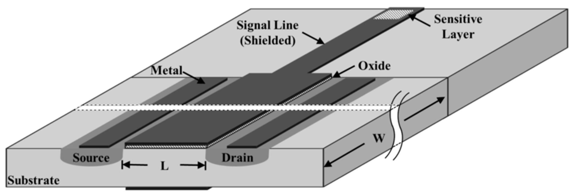
2.1. EGFET Basic Principle
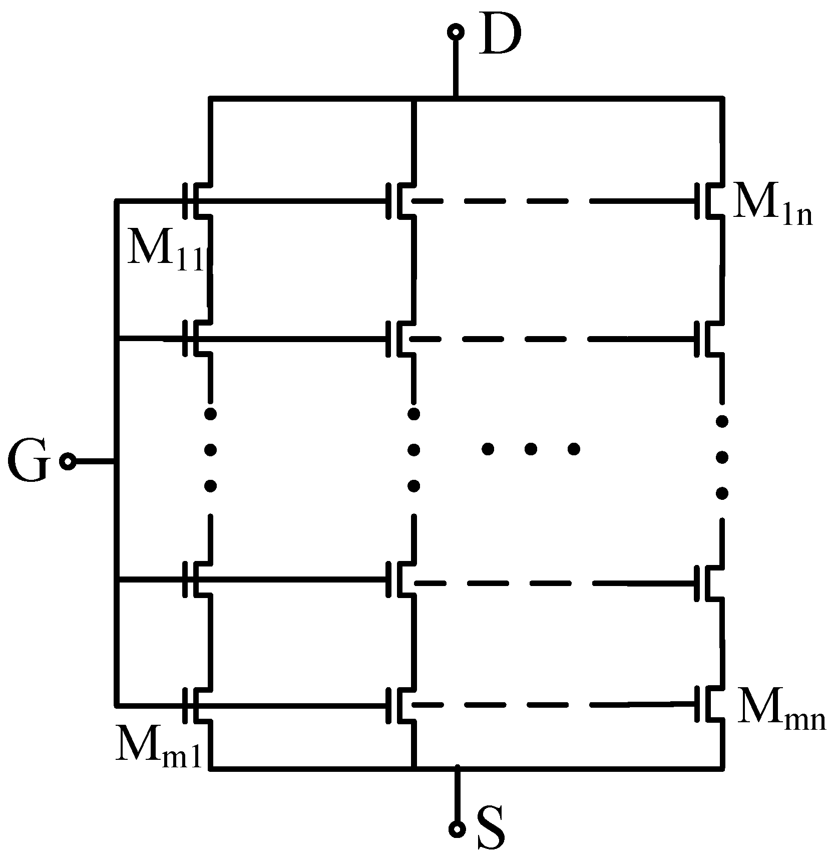
2.2. Circuit Design
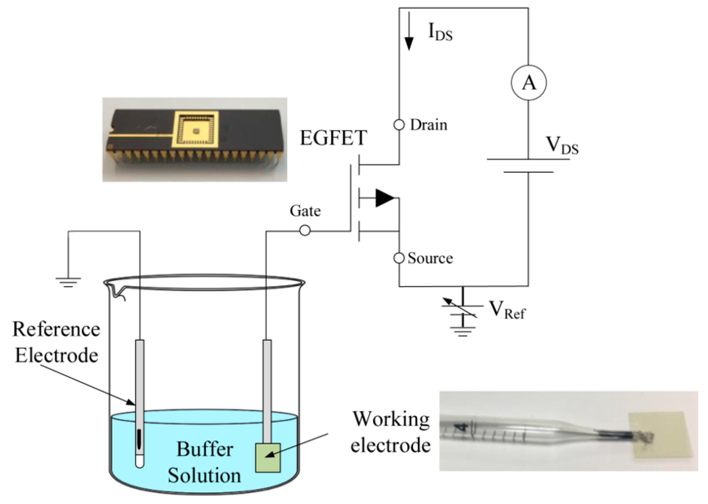
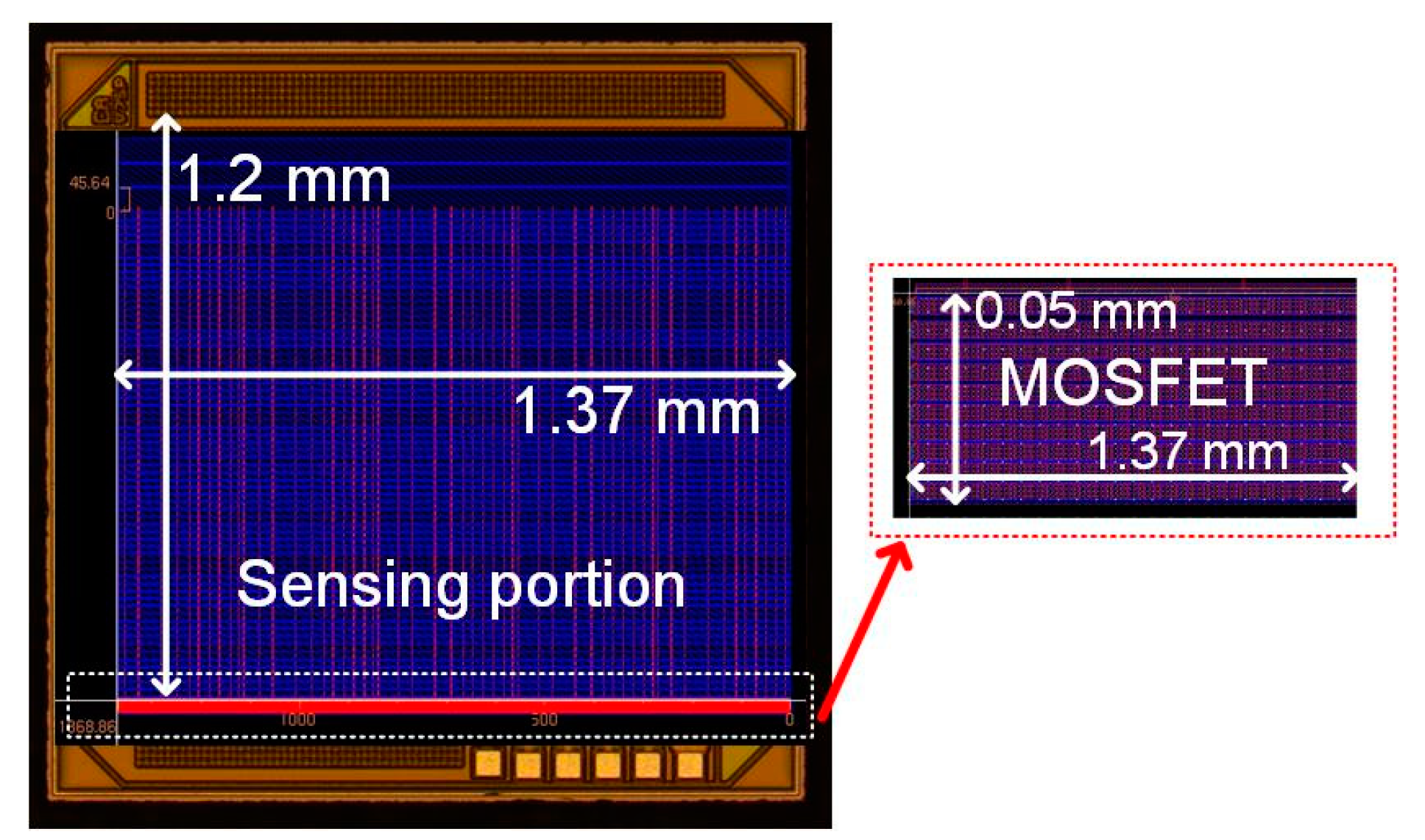
2.3. pH Sensor
3. Results
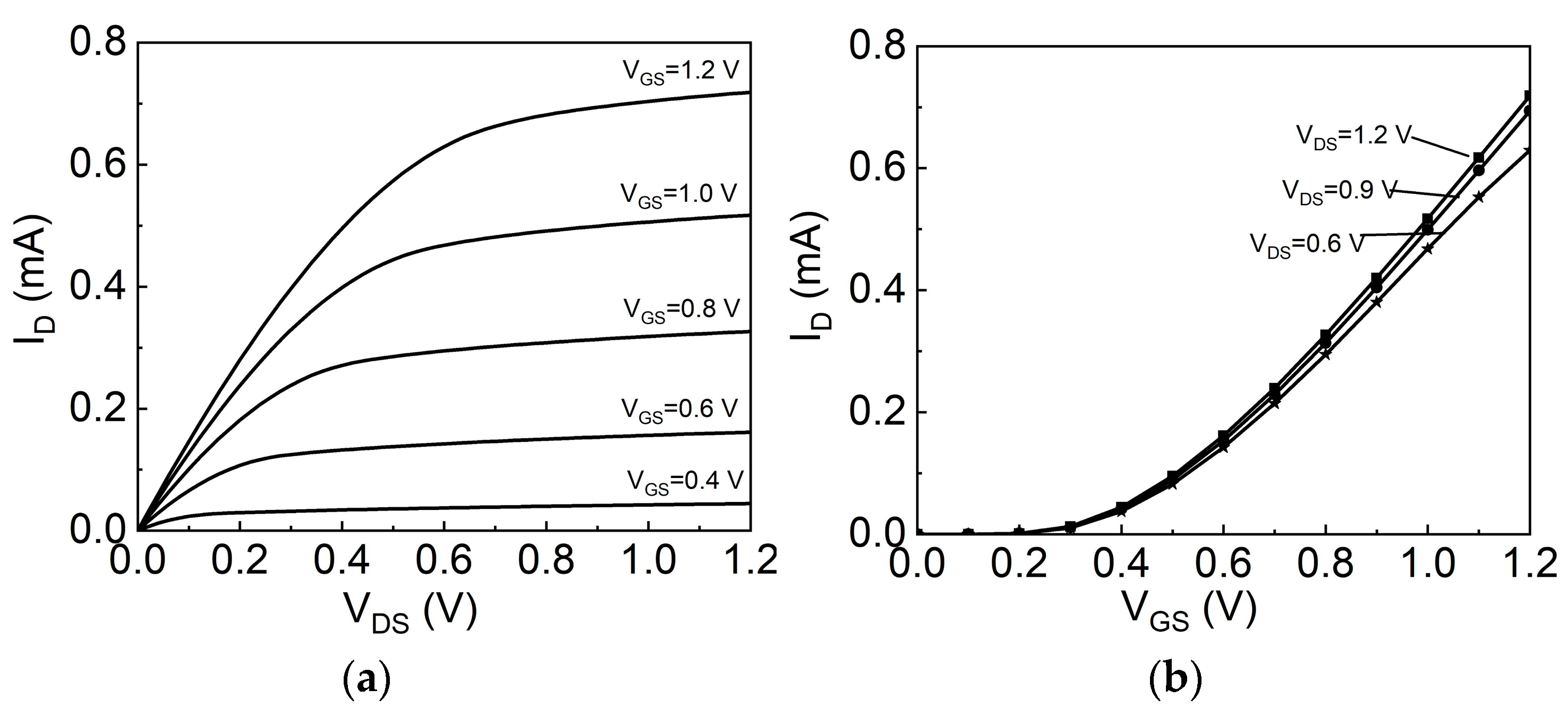
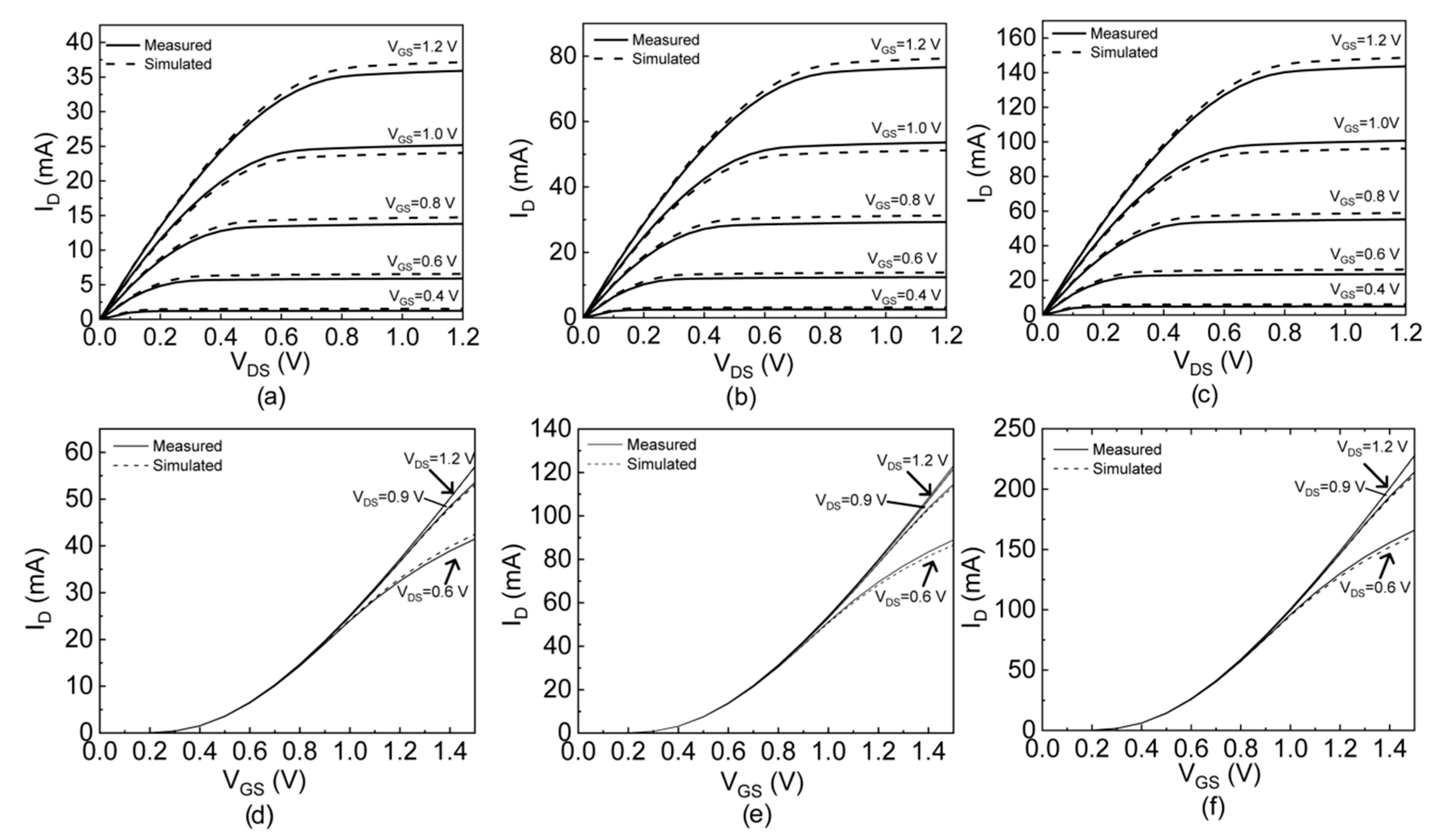
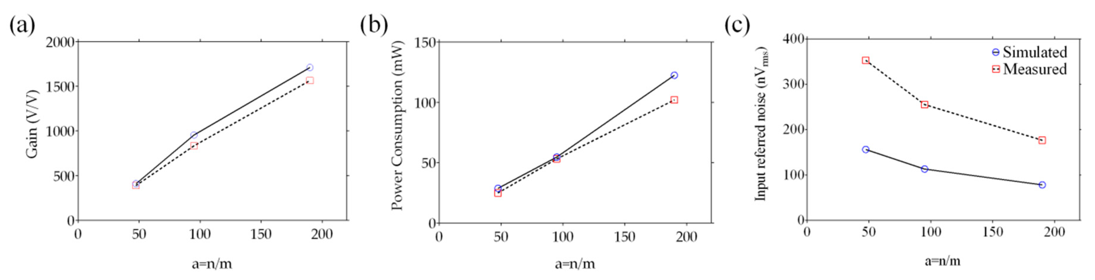
3.1. Simulation and Measurements on EGFET
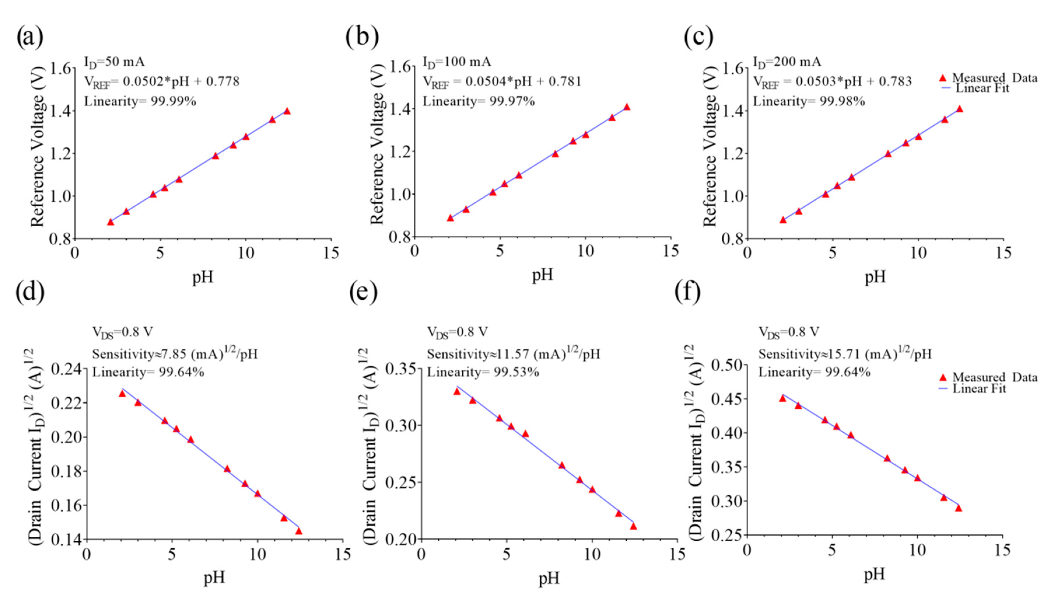
3.2. Characterization of EGFETs as pH Sensors
4. Discussion
5. Conclusions
Author Contributions
Funding
Acknowledgments
Conflicts of Interest
References
- Schöning, M.J.; Poghossian, A. Bio FEDs (Field-Effect Devices): State-of-the-Art and New Directions. Electroanalysis 2006, 18, 1893–1900. [Google Scholar] [CrossRef]
- Lee, C.-S.; Kim, S.K.; Kim, M. Ion-Sensitive Field-Effect Transistor for Biological Sensing. Sensors 2009, 9, 7111–7131. [Google Scholar] [CrossRef] [PubMed]
- Siqueira, J.R.; Fernandes, E.G.R.; de Oliveira, O.N.; Zucolotto, V. Biosensors Based on Field-Effect Devices. In Nanobioelectrochemistry; Crespilho, F., Ed.; Springer: Berlin/Heidelberg, Germany, 2013. [Google Scholar]
- Batista, P.; Mulato, M.; Graeff, C.D.O.; Fernandez, F.; Marques, F.D.C. SnO2 extended gate field-effect transistor as pH sensor. Braz. J. Phys. 2006, 36, 478–481. [Google Scholar] [CrossRef]
- Yang, C.; Wang, I.; Lin, Y.; Huang, C.; Lu, T.; Lue, C.; Pijanowska, D.G.; Hua, M.; Lai, C. Low cost and flexible electrodes with NH3 plasma treatments in extended gate field effect transistors for urea detection. Sens. Actuators B Chem. 2013, 187, 274–279. [Google Scholar] [CrossRef]
- Qi, J.; Zhang, H.; Ji, Z.; Xu, M.; Zhang, Y. ZnO nano-array-based EGFET biosensor for glucose detection. Appl. Phys. A 2015, 119, 807–811. [Google Scholar] [CrossRef]
- Asif, M.; Nur, O.; Willander, M.; Danielsson, B. Selective calcium ion detection with functionalized ZnO nanorods-extended gate MOSFET. Biosens. Bioelectron. 2009, 24, 3379–3382. [Google Scholar] [CrossRef] [PubMed]
- Chen, C.; Ganguly, A.; Lu, C.; Chen, T.; Kuo, C.; Chen, R.; Tu, W.; Fischer, W.B.; Chen, K.; Chen, L. Ultrasensitive in situ label-free DNA detection using a GaN nanowire-based extended-gate field-effect-transistor sensor. Anal. Chem. 2011, 83, 1938–1943. [Google Scholar] [CrossRef] [PubMed]
- Ishige, Y.; Shimoda, M.; Kamahori, M. Extended-gate FET-based enzyme sensor with ferrocenyl-alkanethiol modified gold sensing electrode. Biosens. Bioelectron. 2009, 24, 1096–1102. [Google Scholar] [CrossRef] [PubMed]
- Sung, M.; Shin, K.; Moon, W. A micro-machined hydrophone employing a piezoelectric body combined on the gate of a field-effect transistor. Sens. Actuators A Phys. 2016, 237, 155–166. [Google Scholar] [CrossRef]
- Fiorillo, A.S.; Van Der Spiegel, J.; Bloomfield, P.E.; Esmail-Zandi, D. A P(VDF-TrFE)-based Integrated Ultrasonic Transducer. Sens. Actuators A Phys. 1990, 21–23, 719–725. [Google Scholar] [CrossRef]
- Van der Spiegel, J.; Fiorillo, A.S. Method of Manufacturing Ferroelectric MOSFET Sensors. U.S. Patent US5254504A, 19 October 1993. [Google Scholar]
- Van der Spiegel, J.; Lauks, I.; Chan, P.; Babic, D. The extended gate chemically sensitive field effect transistor as multi-species microprobe. Sens. Actuators 1983, 4, 291–298. [Google Scholar] [CrossRef]
- Van Hal, R.E.G.; Eijkel, J.C.T.; Bergveld, P. A novel description of ISFET sensitivity with the buffer capacity and double-layer capacitance as key parameters. Sens. Actuators B Chem. 1995, 24, 201–205. [Google Scholar] [CrossRef]
- Batista, P.D.; Mulato, M. ZnO extended-gate field-effect transistors as pH sensors. Appl. Phys. Lett. 2005, 87, 143508. [Google Scholar] [CrossRef]
- Yang, C.M.; Wang, J.C.; Chiang, T.W.; Lin, Y.T.; Juan, T.W.; Chen, T.G.; Shih, M.Y.; Lue, C.E.; Lai, C.S. Hydrogen ion sensing characteristics of IGZO/Si electrode in EGFET. Int. J. Nanotechnol. 2013, 11, 15–26. [Google Scholar] [CrossRef]
- Guerra, E.M.; Silva, G.R.; Mulato, M. Extended gate field effect transistor using V2O5 xerogel sensing membrane by sol-gel method. Solid State Sci. 2009, 11, 456–460. [Google Scholar] [CrossRef]
- Brews, J.R.; Fichtner, W.; Nicollian, E.H.; Sze, S.M. Generalized guide for MOSFET miniaturization. IEEE Electron Device Lett. 1980, 1, 2–4. [Google Scholar] [CrossRef]
- Batista, P.D.; Mulato, M. Polycrystalline fluorine-doped tin oxide as sensoring thin film in EGFET pH sensor. J. Mater. Sci. 2010, 45, 5478–5481. [Google Scholar] [CrossRef]
- Lue, C.; Wang, L.; Huang, C.; Shiao, Y.; Wang, H.; Yang, C.; Hsu, H.; Chang, C.; Wang, W.; Lai, C. pH sensing reliability of flexible ITO/PET electrodes on EGFETs prepared by a roll-to-roll process. Microelectron. Reliab. 2012, 52, 1651–1654. [Google Scholar] [CrossRef]
- Chou, J.; Chiang, J.; Wu, C. pH and procaine sensing characteristics of extended-gate field-effect transistor based on indium tin oxide glass. Jpn. J. Appl. Phys. 2005, 44, 4838. [Google Scholar] [CrossRef]
- Chiu, Y.; Tseng, C.; Lee, C. Nanostructured EGFET pH sensors with surface-passivated ZnO thin-film and nanorod array. IEEE Sens. J. 2012, 12, 930–934. [Google Scholar] [CrossRef]
- Lin, M.-Y.; Hsu, W.-Y.; Yang, Y.-S.; Huang, J.-W.; Chung, Y.-L.; Chen, H. Immobilized rolling circle amplification on extended-gate field-effect transistors with integrated readout circuits for early detection of platelet-derived growth factor. Anal. Bioanal. Chem. 2016, 408, 4785–4797. [Google Scholar] [CrossRef] [PubMed]
- Kim, A.; Ah, C.S.; Yu, H.Y.; Yang, J.-H.; Baek, I.-B.; Ahn, C.-G.; Park, C.W.; Jun, M.S.; Lee, S. Ultrasensitive, label-free, and real-time immunodetection using silicon field-effect transistors. Appl. Phys. Lett. 2007, 91, 103901. [Google Scholar] [CrossRef]
- Razmi, N.; Baradaran, B.; Hejazi, M.; Hasanzadeh, M.; Mosafer, J.; Mokhtarzadeh, A.; de la Guardia, M. Recent advances on aptamer-based biosensors to detection of platelet-derived growth factor. Biosens. Bioelectron. 2018, 113, 58–71. [Google Scholar] [CrossRef] [PubMed]
- Pullano, S.A.; Critello, C.D.; Mahbub, I.; Tasneem, N.T.; Shamsir, S.; Islam, S.K.; Greco, M.; Fiorillo, A.S. EGFET-Based Sensors for Bioanalytical Applications: A Review. Sensors 2018, 18, 4042. [Google Scholar] [CrossRef] [PubMed]
- Galup-Montoro, C.; Schneider, M.C.; Loss, I.J.B. Series-Parallel Association of FET’s for High Gain and High Frequency Applications. IEEE J. Solid-State Circuits 1994, 29, 1094–1101. [Google Scholar] [CrossRef]
- Arnaud, A.; Hoffmann, A. A compact model for flicker noise in MOSFETs considering both correlated mobility and carrier number fluctuations. Analog Integr. Circuits Signal Process. 2016, 89, 611–618. [Google Scholar] [CrossRef]
- Chi, L.-L.; Chou, J.-C.; Chung, W.-Y.; Sun, T.-P.; Hsiung, S.-K. Study on extended gate field effect transistor with tin oxide sensing membrane. Mater. Chem. Phys. 2000, 63, 19–23. [Google Scholar] [CrossRef]
- Brouk, I.; Nemirovsky, Y. l/f noise in CMOS transistors for analog applications. IEEE Trans. Electron Devices 2001, 48, 921–927. [Google Scholar]
- Hung, K.K.; Ko, P.K.; Hu, C.; Cheng, Y.C. A unified model for the flicker noise in metal-oxide-semiconductor field-effect transistors. IEEE Trans. Electron Devices 1990, 37, 654–665. [Google Scholar] [CrossRef]
- Tedja, S.; Van Der Spiegel, J.; Williams, H.H. Analytical and Experimental Studies of Thermal Noise in MOSFET’s. IEEE Trans. Electron Devices 1994, 41, 2069–2075. [Google Scholar] [CrossRef]
- Kaisti, M.; Alexandrovna Boeva, Z.; Koskinen, J.; Nieminen, S.; Bobacka, J.; Levon, K. Hand-held transistor based electrical and multiplexed chemical sensing system. ACS Sens. 2016, 1, 1423–1431. [Google Scholar] [CrossRef]
- D’Agostino, F.; Quercia, D. Short-channel effects in MOSFETs. In Introduction to VLSI Design (EECS 467); London’s Global University: London, UK, 2000. [Google Scholar]
- Girardi, A.; Bampi, S. AC analysis of an inverter amplifier using minimum-length trapezoidal association of transistors. Microelectron. Reliab. 2004, 44, 665–671. [Google Scholar] [CrossRef]
- Fog, A.; Buck, R.P. Electronic semiconducting oxides as pH sensors. Sens. Actuators 1984, 5, 137–146. [Google Scholar] [CrossRef]
- Al-Hardan, N.H.; Abdul Hamid, M.A.; Ahmed, N.M.; Jalar, A.; Shamsudin, R.; Othman, N.K.; Kar Keng, L.; Chiu, W.; Al-Rawi, H.N. High Sensitivity pH Sensor Based on Porous Silicon (PSi) Extended Gate Field-Effect Transistor. Sensors 2016, 16, 839. [Google Scholar] [CrossRef] [PubMed]
- Das, A.; Ko, D.H.; Chen, C.-H.; Chang, L.-B.; Lai, C.-S.; Chu, F.-C.; Chow, L.; Lin, R.-M. Highly sensitive palladium oxide thin film extended gate FETs as pH sensor. Sens. Actuators B Chem. 2014, 205, 199–205. [Google Scholar] [CrossRef]
- Yin, L.; Chou, J.; Chung, W.; Sun, T.; Hsiung, S. Study of indium tin oxide thin film for separative extended gate ISFET. Mater. Chem. Phys. 2001, 70, 12–16. [Google Scholar] [CrossRef]
- Fuller, L. SPICE Model for NMOS and PMOS FETs in the CD4007 Chip; Rochester Institute of Technology: Rochester, MN, USA, 2015. [Google Scholar]
- Arafa, H.; Obahiagbon, U.; Kullman, D.; Domínguez, F.; Magee, A.; Christen, J.B. Characterization and application of a discrete quartz extended-gate ISFET for the assessment of tumor cell viability. In Proceedings of the IEEE Healthcare Innovation Point-of-Care Technologies Conference (HI-POCT), Cancun, Mexico, 9–11 November 2016. [Google Scholar]
- BS170 - LTwiki-Wiki for LTspice. Available online: htttp://ltwiki.org/index.php?title=BS170 (accessed on 1 June 2018).
- Guliga, H.; Abdullah, W.F.H.; Herman, S.H. Extended gate field effect transistor (EGFET) integrated readout interfacing circuit for pH sensing. In Proceedings of the IEEE International Conference on Electrical, Electronics and System Engineering (ICEESE), Kuala Lumpur, Malaysia, 9–10 December 2014; pp. 11–14. [Google Scholar]
- Fiorillo, A.S.; Tiriolo, R.; Pullano, S.A. Absorption of Urea into Zeolite Layer Integrated with Microelectronic Circuits. IEEE Trans. Nanotechnol. 2015, 14, 214–217. [Google Scholar] [CrossRef]
- Kaisti, M. Detection principles of biological and chemical FET sensors. Biosens. Bioelectron. 2017, 98, 437–448. [Google Scholar] [CrossRef] [PubMed]
- Zhang, Q.; Kaisti, M.; Prabhu, A.; Yu, Y.; Song, Y.A.; Rafailovich, M.H.; Rahman, A.; Levon, A. Polyaniline-functionalized ion-sensitive floating-gate FETs for the on-chip monitoring of peroxidase-catalyzed redox reactions. Electrochim. Acta 2018, 261, 256–264. [Google Scholar] [CrossRef]
- Yusof, K.A.; Rahman, R.A.; Zulkefle, M.A.; Herman, S.H.; Abdullah, W.F.H. EGFET pH sensor performance dependence on sputtered TiO2 sensing membrane deposition temperature. J. Sens. 2016, 2016, 7594531. [Google Scholar] [CrossRef]
- Wang, J.-L.; Yang, P.-Y.; Hsieh, T.-Y.; Juan, P.-C. Ionic pH and glucose sensors fabricated using hydrothermal ZnO nanostructures. Jpn. J. Appl. Phys. 2015, 55, 01AE16. [Google Scholar] [CrossRef]
- Wu, Y.-C.; Wu, S.-J.; Lin, C.-H. High performance EGFET-based pH sensor utilizing low-cost industrial-grade touch panel film as the gate structure. IEEE Sens. J. 2015, 15, 6279–6286. [Google Scholar] [CrossRef]
- Yin, L.-T.; Wang, H.-Y.; Lin, Y.-C.; Huang, W.-C. A novel instrumentation circuit for electrochemical measurements. Sensors 2012, 12, 9687–9696. [Google Scholar] [CrossRef] [PubMed]
- Batista, P.D. An embedded measurement system for electrical characterization of EGFET as pH sensor. Meas. Sci. Technol. 2013, 25, 027001. [Google Scholar] [CrossRef]
- Chien, Y.-S.; Tsai, W.-L.; Lee, I.-C.; Chou, J.-C.; Cheng, H.-C. A novel pH sensor of extended-gate field-effect transistors with laser-irradiated carbon-nanotube network. IEEE Electron Device Lett. 2012, 33, 1622–1624. [Google Scholar] [CrossRef]


| [6,39,40] | [41,42] | [23] | [43] | This Work #1 | This Work #2 | This Work #3 | |
|---|---|---|---|---|---|---|---|
| W/L (µm/µm) | PMOS: 360/10 NMOS: 170/10 | 9700/2 | 18/1 | NR | 2000/10 | 4000/10 | 8000/10 |
| Type | CD4007UB | BS170 | CMOS | CMOS | NMOS | NMOS | NMOS |
| Process (µm) | C | C | 0.35 | 0.13 | 0.13 | 0.13 | 0.13 |
| Input referred noise (nVrms) | NR | NR | 1.58E6 | 4258 (@100 Hz) | 252.7 (0.1 to 10 Hz) | 255.1 (0.1 to 10 Hz) | 176.4 (0.1 to 10 Hz) |
| Power (mW) | 100 | 350 | NR | 3.77 | 24.99 | 53.23 | 102.0 |
| Electrode | Range | Sensitivity (mV/pH) | Linearity (%) | Reference Electrode | FET Device | Reference |
|---|---|---|---|---|---|---|
| ITO/PET | 2.1–12.1 | 45.9–52.3 | 98.3–99.6 | Ag/AgCl | CD4007UB | [5] |
| InGaZnO | 2–10 | 59.5 | 99.7 | Ag/AgCl | CD4007 | [16] |
| V2O5 | 2–10 | 58.1 ± 0.8 | nr | nr | CD4007UB | [17] |
| ITO/PET | 2–12 | 50.1 ± 1.7 | 98.5 | Ag/AgCl | CD4007CN | [20] |
| SnO2 | 2–12 | 56–58 | nr | SCE | CD4007UB or LF356N | [29] |
| PdO | 2–12 | 62.87 ± 2 | 99.97 | Ag/AgCl | CD4007UBE | [38] |
| ITO | 2–12 | 58 | nr | SCE | CD4007UB | [39] |
| TiO2 | 1.8–12 | 59.89 | 93.50 | Ag/AgCl | NDP6060L | [47] |
| AZO | 1–13 | 57.95 | 99.98 | Ag/AgCl | CD4007UB | [48] |
| ITO/SiO2/Nb2O5 | 3–13 | 59.2 | 99.48 | Ag/AgCl | IC4007 | [49] |
| SnO2/ITO/PET | 2–12 | 53.8–58.7 | nr | Ag/AgCl | LT1167–I.A. | [50] |
| Glass | 2–12 | 55 | nr | nr | CD4007UB | [51] |
| CNT | 3–13 | 50.9 | 99.78 | nr | nr | [52] |
| ITO | 2–12 | 50.2 | 99.9 | Ag/AgCl | 130nm CMOS | This work |
© 2019 by the authors. Licensee MDPI, Basel, Switzerland. This article is an open access article distributed under the terms and conditions of the Creative Commons Attribution (CC BY) license (http://creativecommons.org/licenses/by/4.0/).
Share and Cite
Pullano, S.A.; Tasneem, N.T.; Mahbub, I.; Shamsir, S.; Greco, M.; Islam, S.K.; Fiorillo, A.S. Deep Submicron EGFET Based on Transistor Association Technique for Chemical Sensing. Sensors 2019, 19, 1063. https://doi.org/10.3390/s19051063
Pullano SA, Tasneem NT, Mahbub I, Shamsir S, Greco M, Islam SK, Fiorillo AS. Deep Submicron EGFET Based on Transistor Association Technique for Chemical Sensing. Sensors. 2019; 19(5):1063. https://doi.org/10.3390/s19051063
Chicago/Turabian StylePullano, Salvatore A., Nishat T. Tasneem, Ifana Mahbub, Samira Shamsir, Marta Greco, Syed K. Islam, and Antonino S. Fiorillo. 2019. "Deep Submicron EGFET Based on Transistor Association Technique for Chemical Sensing" Sensors 19, no. 5: 1063. https://doi.org/10.3390/s19051063
APA StylePullano, S. A., Tasneem, N. T., Mahbub, I., Shamsir, S., Greco, M., Islam, S. K., & Fiorillo, A. S. (2019). Deep Submicron EGFET Based on Transistor Association Technique for Chemical Sensing. Sensors, 19(5), 1063. https://doi.org/10.3390/s19051063