
Nitride-Based Materials for Flexible MEMS Tactile and Flow Sensors in Robotics

 ,
,
Abstract
:1. Introduction
2. Materials
2.1. Silicon Nitride Stressor Layer
2.2. Aluminum Nitride Stressor Layer
2.3. Piezoelectric Properties of Aluminum Nitride
3. Methods
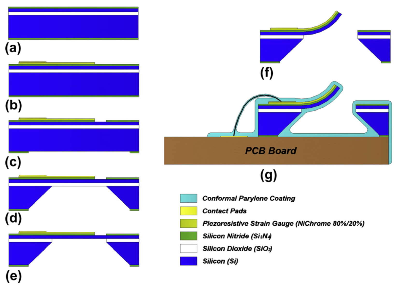
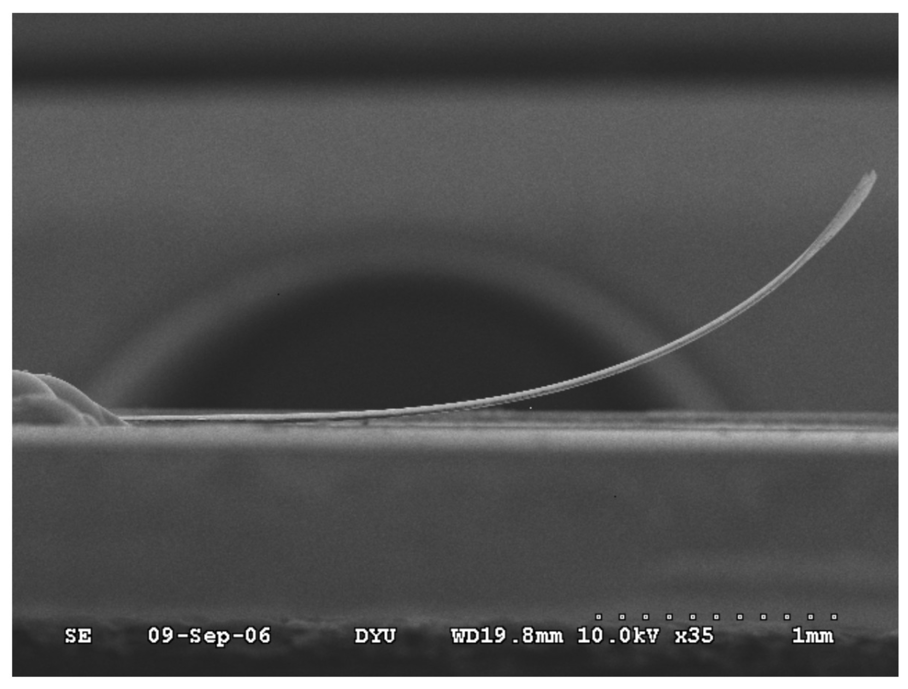
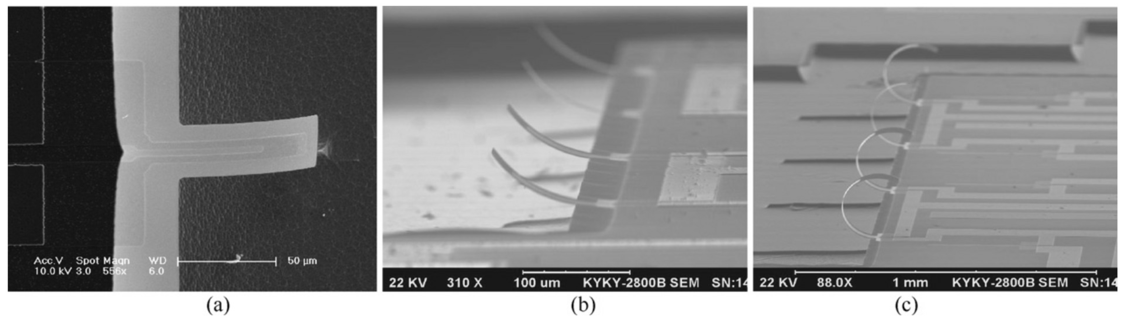
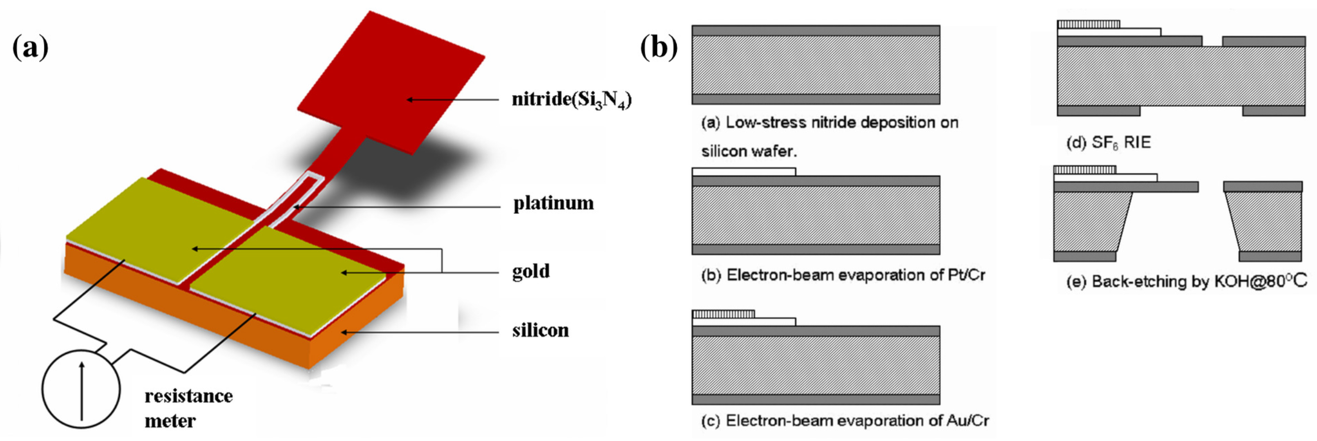
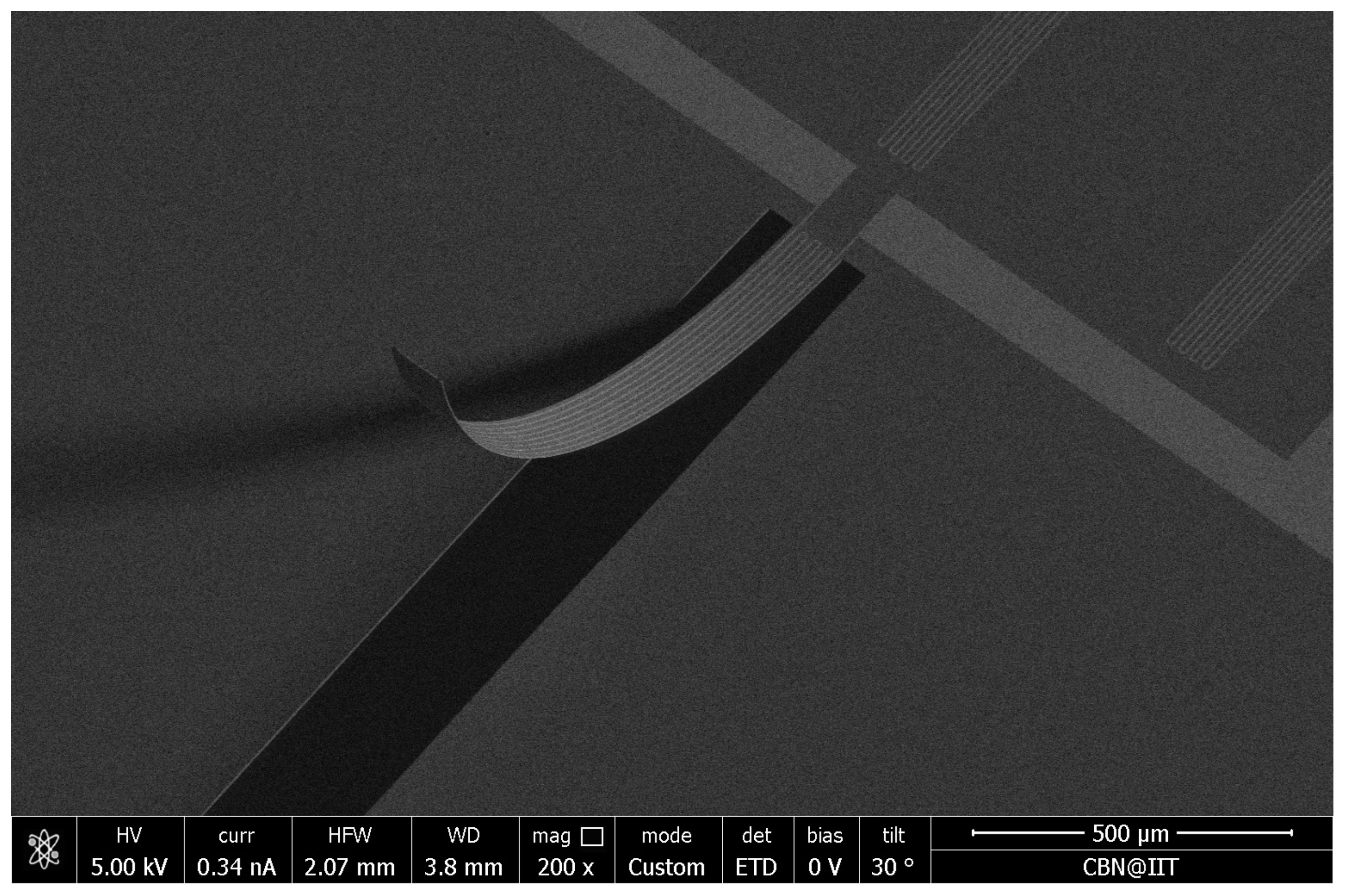
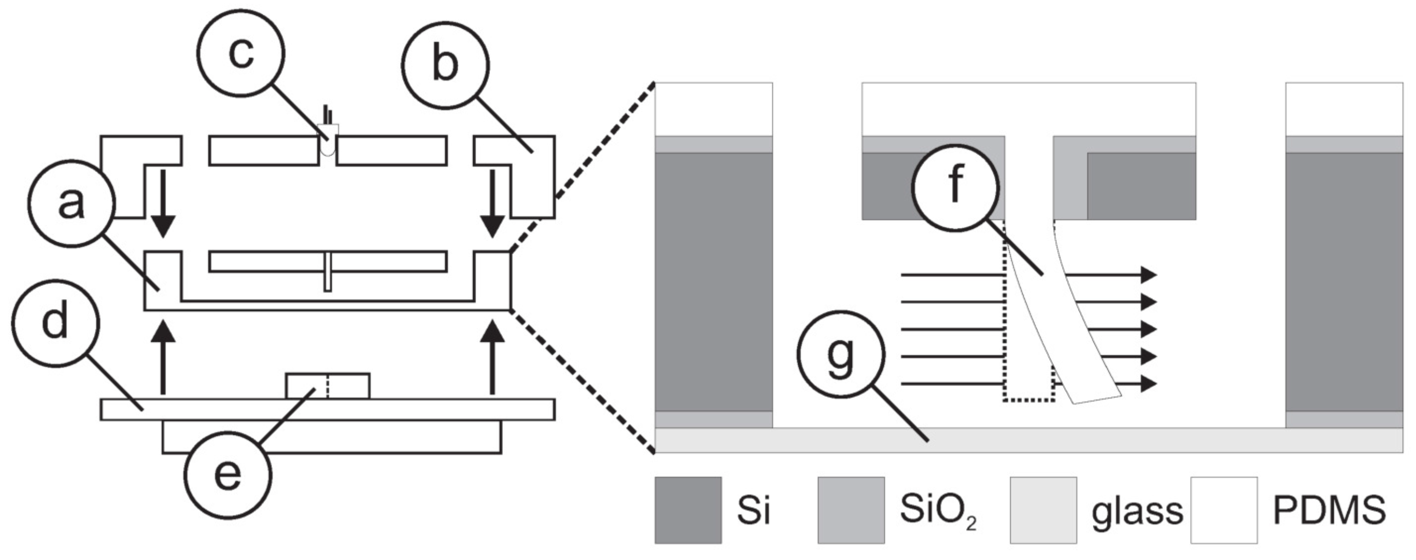
3.1. Microfabrication of Piezoresistive Upwards-Bent Cantilever Beams
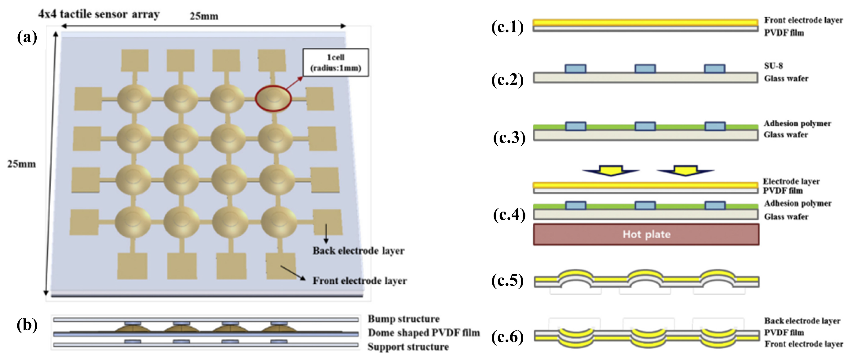
3.2. Microfabrication of Piezoelectric Tactile Membranes
4. Results and Applications
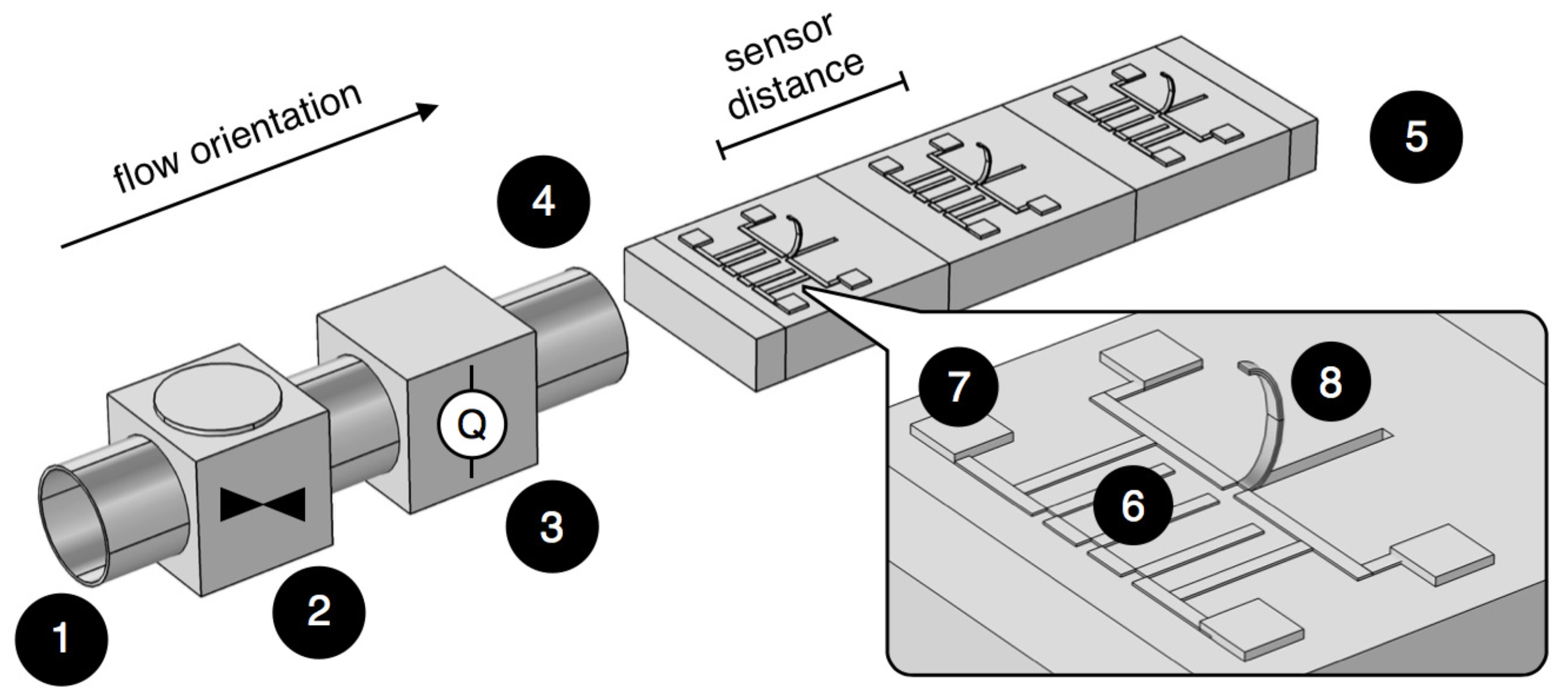
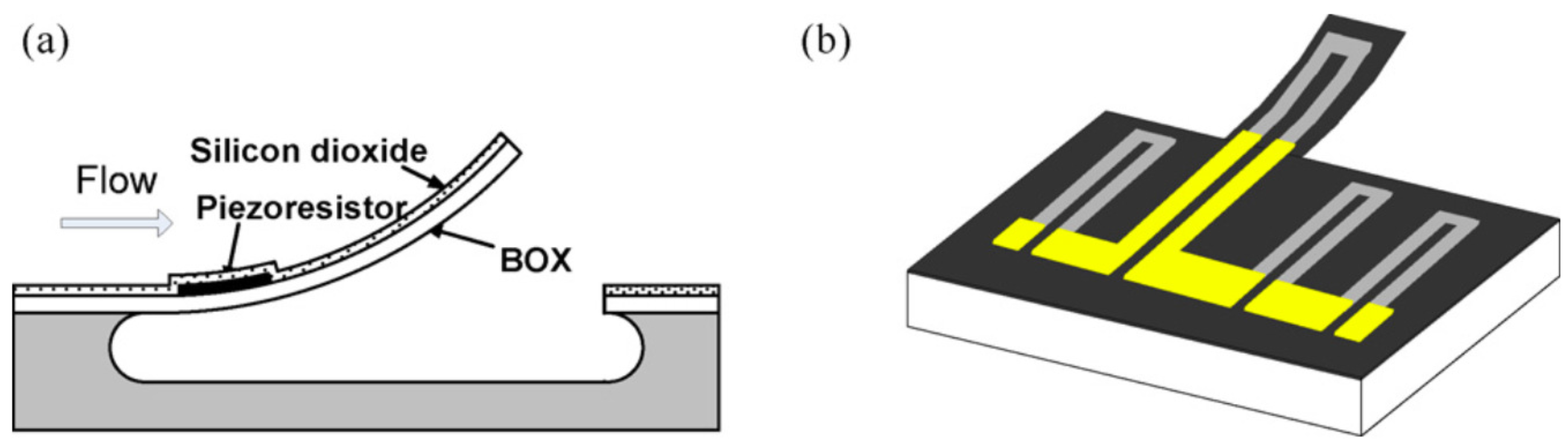
4.1. Piezoresistive Flow Sensing: Mimicking the Biological Lateral Line Organ
4.1.1. Bio-Inspired Artificial Hair Cells
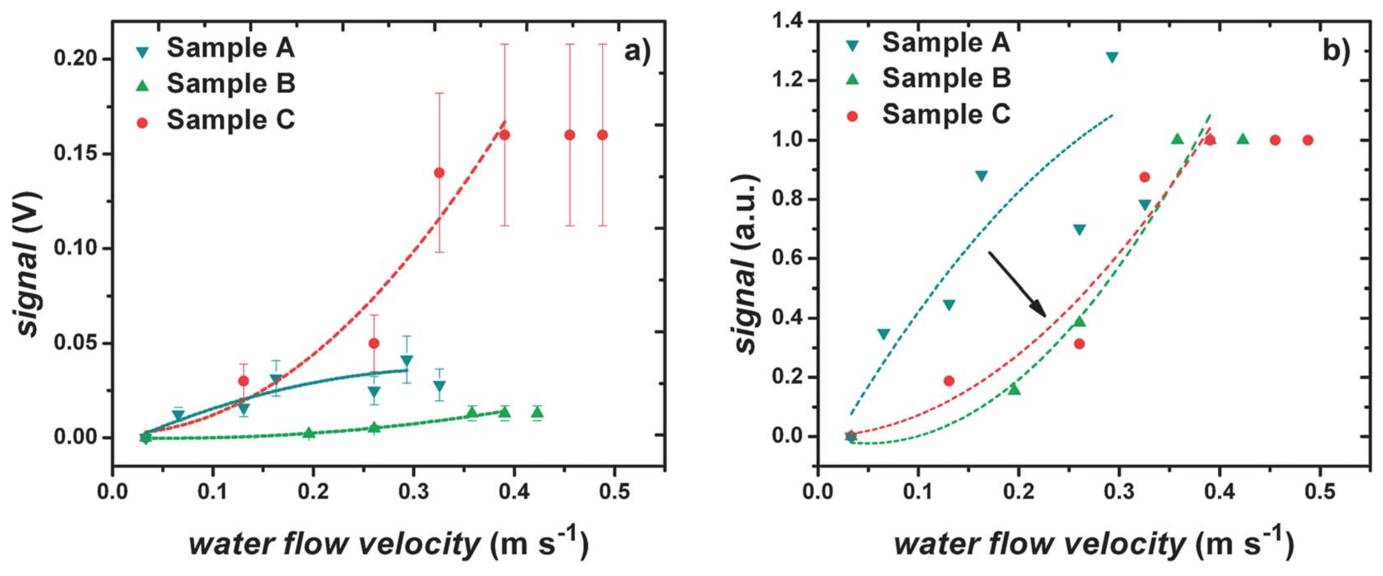
4.1.2. Artificial Lateral Line Flow Rate and Velocity Sensing
4.2. Piezoelectric Tactile Sensing: Mimicking the Human Tactile Sense
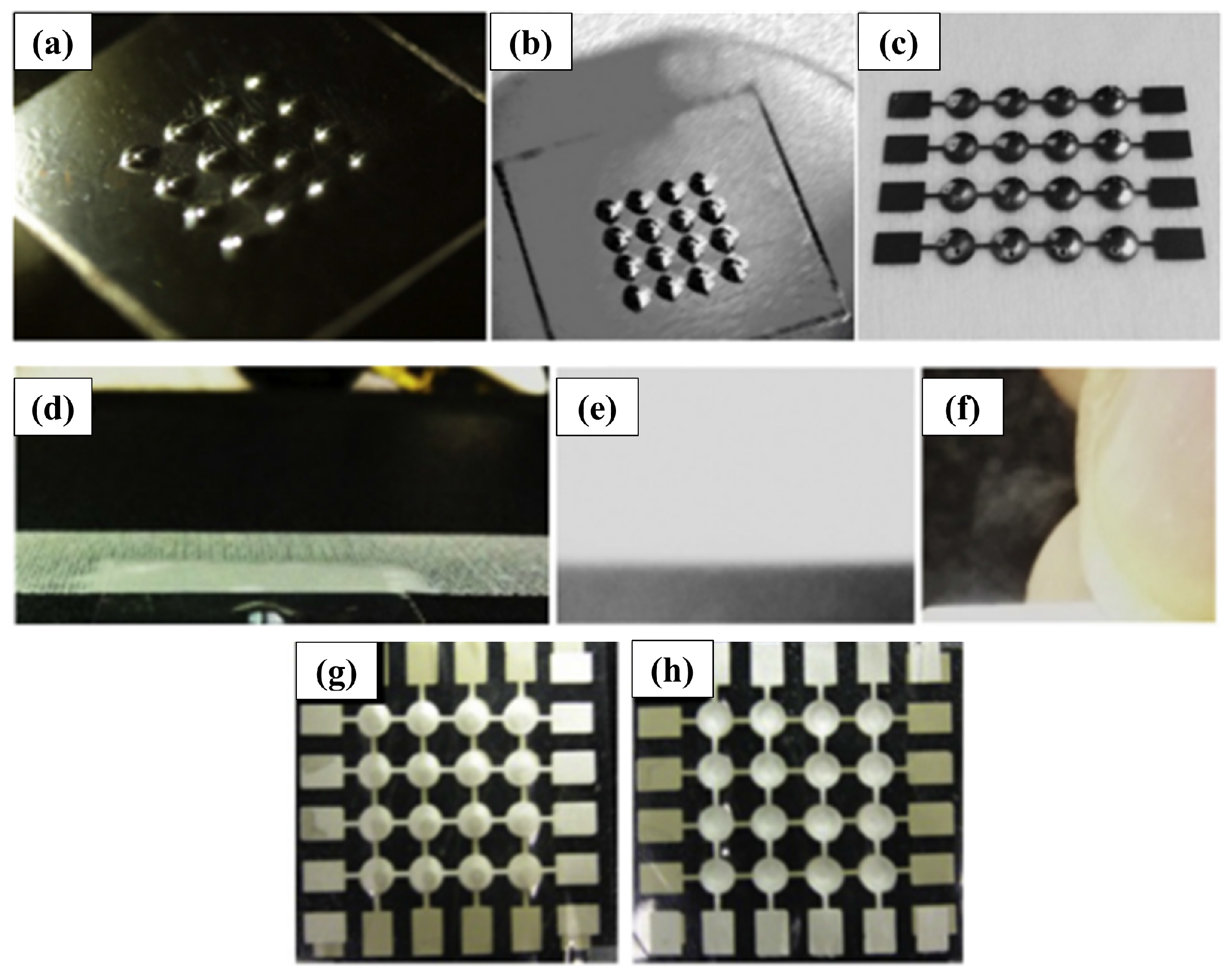
4.2.1. Tactile Sensors
4.2.2. Tactile Sensing System
5. Conclusions
Acknowledgments
Author Contributions
Conflicts of Interest
Abbreviations
| AlN | Aluminum Nitride |
| CCC | Cross-Correlation Coefficient |
| CCF | Cross-Correlation Function |
| CMOS | Complementary Metal-Oxide-Semiconductor |
| CMP | Chemical Mechanical Polishing |
| COC | Cyclic Olefin Copolymer |
| CVP | Chemical Vapor Deposition |
| Cr | Chrome |
| DRIE | Deep Reactive Ion Etching |
| DSDT | Dome-Shaped Diaphragm Transducer |
| ICP | Inductively Coupled Plasma |
| KOH | Potassium Hydroxide |
| LPCVD | Low Pressure Chemical Vapor Deposition |
| LTO | Low Temperature Oxide |
| MEMS | Micro-Electro-Mechanical Systems |
| Mo | Molybdenum |
| PECVD | Plasma-Enhanced Chemical Vapor Deposition |
| pMUT | Piezoelectric Micromachined Ultrasonic Transducers |
| PVDF | Polyvinylidene Difluoride |
| PZT | Lead Zirconate Titanate |
| RIE | Reactive Ion Etching |
| SF6 | Sulfur Hexafluoride |
| Si | Silicon |
| SiCl | Silicon Tetrachloride |
| SiN | Silicon Nitride |
| SiO | Silicon Dioxide |
| SOI | Silicon-On-Insulator |
| TrFE | Trifluoroethylene |
| UT | Ultrasonic Transducer |
| VDF | Vinylidene Fluoride |
| ZnO | Zinc Oxide |
References
- Bao, M. Analysis and Design Principles of MEMS Devices; Elsevier: Amsterdam, The Netherlands, 2005. [Google Scholar]
- Judy, J.W. Microelectromechanical systems (MEMS): Fabrication, design and applications. Smart Mater. Struct. 2001, 10, 1115–1134. [Google Scholar] [CrossRef]
- Liu, C. Foundations of MEMS, 2nd ed.; Pearson: Upper Saddle River, NJ, USA, 2012. [Google Scholar]
- Cai, S.; Breid, D.; Crosby, A.; Suo, Z.; Hutchinson, J. Periodic patterns and energy states of buckled films on compliant substrates. J. Mech. Phys. Solids 2011, 59, 1094–1114. [Google Scholar] [CrossRef]
- Gioia, G.; Ortiz, M. Delamination of compressed thin films. Adv. Appl. Mech. 1997, 33, 119–192. [Google Scholar]
- Freund, L.B.; Suresh, S. Thin Film Materials: Stress, Defect Formation and Surface Evolution; Cambridge University Press: Cambridge, UK, 2004. [Google Scholar]
- Wang, Y.H.; Lee, C.Y.; Chiang, C.M. A MEMS-based Air Flow Sensor with a Free-standing Micro-cantilever Structure. Sensors 2007, 7, 2389–2401. [Google Scholar] [CrossRef]
- Kao, I.; Kumar, A.; Binder, J. Smart MEMS Flow Sensor: Theoretical Analysis and Experimental Characterization. IEEE Sens. J. 2007, 7, 713–722. [Google Scholar] [CrossRef]
- Zhang, Q.; Ruan, W.; Wang, H.; Zhou, Y.; Wang, Z.; Liu, L. A self-bended piezoresistive microcantilever flow sensor for low flow rate measurement. Sens. Actuators A 2010, 158, 273–279. [Google Scholar] [CrossRef]
- Rizzi, F.; Qualtieri, A.; Chambers, L.D.; Epifani, G.; Megill, W.M.; De Vittorio, M. Stress-Driven Artificial Hair Cell for Flow Sensing. In Flow Sensing in Air and Water: Behavioral, Neural and Engineering Principles of Operation; Bleckmann, H., Mogdans, J., Coombs, S.L., Eds.; Springer: Berlin, Germany, 2014; pp. 499–519. [Google Scholar]
- Claassen, W.; Valkenburg, W.; Willemsen, M.; vd Wijgert, W. Influence of deposition temperature, gas pressure, gas phase composition, and RF frequency on composition and mechanical stress of plasma silicon nitride layers. J. Electrochem. Soc. 1985, 132, 893–898. [Google Scholar] [CrossRef]
- Franz, G. Low Pressure Plasmas and Microstructuring Technology; Springer: Berlin/Heidelberg, Germany, 2009. [Google Scholar]
- Reif, R.; Kern, W. IV-1—Plasma-Enhanced Chemical Vapor Deposition. In Thin Film Processes; Vossen, J.L., Kern, W., Eds.; Academic Press: San Diego, CA, USA, 1991; pp. 525–564. [Google Scholar]
- Rizzi, F.; Qualtieri, A.; Chambers, L.D.; Megill, W.M.; de Vittorio, M. Parylene conformal coating encapsulation as a method for advanced tuning of mechanical properties of an artificial hair cell. Soft Matter 2013, 9, 2584–2588. [Google Scholar] [CrossRef]
- Wang, Y.H.; Hsueh, T.H.; Ma, R.H.; Lee, C.Y.; Fu, L.M.; Chou, P.C.; Tsai, C.H. A microcantilever-based gas flow sensor for flow rate and direction detection. In Proceedings of the 2008 Symposium on Design, Test, Integration and Packaging of MEMS/MOEMS, Nice, France, 9–11 April 2008; pp. 142–145. [Google Scholar]
- Dubois, M.A.; Muralt, P. Stress and piezoelectric properties of aluminum nitride thin films deposited onto metal electrodes by pulsed direct current reactive sputtering. J. Appl. Phys. 2001, 89, 6389–6395. [Google Scholar] [CrossRef]
- Iborra, E.; Olivares, J.; Clement, M.; Vergara, L.; Sanz-Hervás, A.; Sangrador, J. Piezoelectric properties and residual stress of sputtered AlN thin films for {MEMS} applications. Sens. Actuators A 2004, 115, 501–507. [Google Scholar] [CrossRef]
- Giordano, C.; Ingrosso, I.; Todaro, M.; Maruccio, G.; Guido, S.D.; Cingolani, R.; Passaseo, A.; de Vittorio, M. AlN on polysilicon piezoelectric cantilevers for sensors/actuators. Microelectron. Eng. 2009, 86, 1204–1207. [Google Scholar] [CrossRef]
- Petroni, S.; Tegola, C.L.; Caretto, G.; Campa, A.; Passaseo, A.; De Vittorio, M.; Cingolani, R. Aluminum Nitride piezo-MEMS on polyimide flexible substrates. Microelectron. Eng. 2011, 88, 2372–2375. [Google Scholar] [CrossRef]
- Ababneh, A.; Alsumady, M.; Seidel, H.; Manzaneque, T.; Hernando-García, J.; Sánchez-Rojas, J.; Bittner, A.; Schmid, U. c-axis orientation and piezoelectric coefficients of AlN thin films sputter-deposited on titanium bottom electrodes. Appl. Surf. Sci. 2012, 259, 59–65. [Google Scholar] [CrossRef]
- Jin, H.; Zhou, J.; Dong, S.; Feng, B.; Luo, J.; Wang, D.; Milne, W.; Yang, C. Deposition of c-axis orientation aluminum nitride films on flexible polymer substrates by reactive direct-current magnetron sputtering. Thin Solid Films 2012, 520, 4863–4870. [Google Scholar] [CrossRef]
- Jackson, N. Influence of silicon crystal orientation on piezoelectric textured aluminium nitride deposited on metal electrodes. Vacuum 2016, 132, 47–52. [Google Scholar] [CrossRef]
- Jackson, N.; Mathewson, A. Enhancing the piezoelectric properties of flexible hybrid AlN materials using semi-crystalline parylene. Smart Mater. Struct. 2017, 26, 045005. [Google Scholar] [CrossRef]
- Jang, J.; Jang, J.H.; Choi, H. Piezoelectric ALN cantilever array on a SU-8 substrate for flexible artificial basilar membrane. In Proceedings of the 2017 IEEE 30th International Conference on Micro Electro Mechanical Systems (MEMS), Las Vegas, NV, USA, 22–26 February 2017; pp. 1200–1203. [Google Scholar]
- Andrei, A.; Krupa, K.; Jozwik, M.; Delobelle, P.; Hirsinger, L.; Gorecki, C.; Nieradko, L.; Meunier, C. AlN as an actuation material for {MEMS} applications: The case of AlN driven multilayered cantilevers. Sens. Actuators A 2008, 141, 565–576. [Google Scholar] [CrossRef]
- Qualtieri, A.; Rizzi, F.; Todaro, M.; Passaseo, A.; Cingolani, R.; De Vittorio, M. Stress-driven AlN cantilever-based flow sensor for fish lateral line system. Microelectron. Eng. 2011, 88, 2376–2378. [Google Scholar] [CrossRef]
- Mastronardi, V.M.; Ceseracciu, L.; Guido, F.; Rizzi, F.; Athanassiou, A.; De Vittorio, M.; Petroni, S. Low stiffness tactile transducers based on AlN thin film and polyimide. Appl. Phys. Lett. 2015, 106, 162901. [Google Scholar] [CrossRef]
- Mastronardi, V.M.; Guido, F.; Amato, M.; de Vittorio, M.; Petroni, S. Piezoelectric ultrasonic transducer based on flexible AlN. Microelectron. Eng. 2014, 121, 59–63. [Google Scholar] [CrossRef]
- Li, C.; Wu, P.M.; Lee, S.; Gorton, A.; Schulz, M.J.; Ahn, C.H. Flexible Dome and Bump Shape Piezoelectric Tactile Sensors Using PVDF-TrFE Copolymer. J. Microelectromech. Syst. 2008, 17, 334–341. [Google Scholar]
- Kim, M.S.; Ahn, H.R.; Lee, S.; Kim, C.; Kim, Y.J. A dome-shaped piezoelectric tactile sensor arrays fabricated by an air inflation technique. Sens. Actuators A 2014, 212, 151–158. [Google Scholar] [CrossRef]
- Khan, S.; Tinku, S.; Lorenzelli, L.; Dahiya, R.S. Flexible Tactile Sensors Using Screen-Printed P(VDF-TrFE) and MWCNT/PDMS Composites. IEEE Sens. J. 2015, 15, 3146–3155. [Google Scholar] [CrossRef]
- Dahiya, R.S.; Valle, M.; Metta, G.; Lorenzelli, L.; Pedrotti, S. Deposition, processing and characterization of P (VDF-TrFE) thin films for sensing applications. In Proceedings of the 2008 on Sensors, Lecce, Italy, 26–29 October 2008; pp. 490–493. [Google Scholar]
- Maita, F.; Maiolo, L.; Pecora, A.; Minotti, A.; Fortunato, G.; Smecca, E.; Alberti, A. Low-temperature flexible piezoelectric AlN capacitor integrated on ultra-flexible poly-Si TFT for advanced tactile sensing. In Proceedings of the Sensors, Valencia, Spain, 2–5 November 2014; pp. 1730–1733. [Google Scholar]
- Jackson, N.; Keeney, L.; Mathewson, A. Flexible-CMOS and biocompatible piezoelectric AlN material for MEMS applications. Smart Mater. Struct. 2013, 22, 115033. [Google Scholar] [CrossRef]
- Ma, W. Flexoelectricity: strain gradient effects in ferroelectrics. Phys. Scr. 2007, 2007, 180–183. [Google Scholar] [CrossRef]
- Zubko, P.; Catalan, G.; Tagantsev, A.K. Flexoelectric Effect in Solids. Annu. Rev. Mater. Res. 2013, 43, 387–421. [Google Scholar] [CrossRef]
- Zhou, Y.; Wang, Z.; Wang, C.; Ruan, W.; Liu, L. Design, fabrication and characterization of a two-step released silicon dioxide piezoresistive microcantilever immunosensor. J. Micromech. Microeng. 2009, 19, 065026. [Google Scholar] [CrossRef]
- Qualtieri, A.; Rizzi, F.; Epifani, G.; Ernits, A.; Kruusmaa, M.; De Vittorio, M. Parylene-coated bioinspired artificial hair cell for liquid flow sensing. Microelectron. Eng. 2012, 98, 516–519. [Google Scholar] [CrossRef]
- Dagdeviren, C.; Su, Y.; Joe, P.; Yona, R.; Liu, Y.; Kim, Y.S.; Huang, Y.; Damadoran, A.R.; Xia, J.; Martin, L.W.; et al. Conformable amplified lead zirconate titanate sensors with enhanced piezoelectric response for cutaneous pressure monitoring. Nat. Commun. 2014, 5, 4496. [Google Scholar] [CrossRef] [PubMed]
- Lee, J.; Choi, W.; Yoo, Y.K.; Hwang, K.S.; Lee, S.M.; Kang, S.; Kim, J.; Lee, J.H. A Micro-Fabricated Force Sensor Using an All Thin Film Piezoelectric Active Sensor. Sensors 2014, 14, 22199–22207. [Google Scholar] [CrossRef] [PubMed]
- Goericke, F.; Mansukhani, K.; Yamamoto, K.; Pisano, A. Experimentally validated aluminum nitride based pressure, temperature and 3-axis acceleration sensors integrated on a single chip. In Proceedings of the 2014 IEEE 27th International Conference on Micro Electro Mechanical Systems (MEMS), San Francisco, CA, USA, 26–30 January 2014; pp. 729–732. [Google Scholar]
- Feng, G.H. A piezoelectric dome-shaped-diaphragm transducer for microgenerator applications. Smart Mater. Struct. 2007, 16, 2636–2644. [Google Scholar] [CrossRef]
- Akhbari, S.; Sammoura, F.; Yang, C.; Heidari, A.; Horsley, D.; Lin, L. Self-curved diaphragms by stress engineering for highly responsive pMUT. In Proceedings of the 28th IEEE International Conference on Micro Electro Mechanical Systems (MEMS), Estoril, Portugal, 18–22 January 2015; pp. 837–840. [Google Scholar]
- Bleckmann, H.; Mogdans, J.; Coombs, S.L. (Eds.) Flow Sensing in Air and Water; Springer: Berlin, Germany, 2014. [Google Scholar]
- Coombs, S.; Bleckmann, H.; Fay, R.; Popper, A. (Eds.) The Lateral Line System; Springer: New York, NY, USA, 2014. [Google Scholar]
- McHenry, M.J.; Liao, J.C. The Hydrodynamics of Flow Stimuli. In The Lateral Line System; Coombs, S., Bleckmann, H., Fay, R.R., Popper, A.N., Eds.; Springer: New York, NY, USA, 2014; pp. 73–98. [Google Scholar]
- Nawi, M.N.M.; Manaf, A.A.; Arshad, M.R.; Sidek, O. Review of MEMS flow sensors based on artificial hair cell sensor. Microsyst. Technol. 2011, 17, 1417–1426. [Google Scholar] [CrossRef]
- Tao, J.; Yu, X.B. Hair flow sensors: From bio-inspiration to bio-mimicking—A review. Smart Mater. Struct. 2012, 21, 113001. [Google Scholar] [CrossRef]
- Shizhe, T. Underwater artificial lateral line flow sensors. Microsyst. Technol. 2014, 20, 2123–2136. [Google Scholar] [CrossRef]
- Rizzi, F.; Qualtieri, A.; Dattoma, T.; Epifani, G.; De Vittorio, M. Biomimetics of underwater hair cell sensing. Microelectron. Eng. 2015, 132, 90–97. [Google Scholar] [CrossRef]
- Liu, G.; Wang, A.; Wang, X.; Liu, P. A Review of Artificial Lateral Line in Sensor Fabrication and Bionic Applications for Robot Fish. Appl. Bionics Biomech. 2016, 2016, 4732703. [Google Scholar] [CrossRef] [PubMed]
- Yilmazoglu, O.; Yadav, S.; Cicek, D.; Schneider, J.J. A nano-microstructured artificial-hair-cell-type sensor based on topologically graded 3D carbon nanotube bundles. Nanotechnology 2016, 27, 365502. [Google Scholar] [CrossRef] [PubMed]
- Ozaki, Y.; Ohyama, T.; Yasuda, T.; Shimoyama, I. An air flow sensor modeled on wind receptor hairs of insects. In Proceedings of the IEEE Thirteenth Annual International Conference on Micro Electro Mechanical Systems (Cat. No.00CH36308), Miyazaki, Japan, 27 January 2000; pp. 531–536. [Google Scholar]
- Fan, Z.; Chen, J.; Zou, J.; Bullen, D.; Liu, C.; Delcomyn, F. Design and fabrication of artificial lateral line flow sensors. J. Micromech. Microeng. 2002, 12, 655–661. [Google Scholar] [CrossRef]
- Chen, J.; Fan, Z.; Zou, J.; Engel, J.; Liu, C. Two-Dimensional Micromachined Flow Sensor Array for Fluid Mechanics Studies. J. Aerosp. Eng. 2003, 16, 85–97. [Google Scholar] [CrossRef]
- Engel, J.M.; Chen, J.; Bullen, D.; Liu, C. Polyurethane rubber as a MEMS material: characterization and demonstration of an all-polymer two-axis artificial hair cell flow sensor. In Proceedings of the 18th IEEE International Conference on Micro Electro Mechanical Systems, Miami Beach, FL, USA, 30 January–3 February 2005; pp. 279–282. [Google Scholar]
- Tucker, C.; Chen, N.; Engel, J.; Yang, Y.; Pandya, S.; Liu, C. High-Sensitivity Bi-Directional Flow Sensor Based on Biological Inspiration of Animal Haircell Sensors. In Proceedings of the 5th IEEE Conference on Sensors, Daegu, Korea, 22–25 October 2006; pp. 1440–1442. [Google Scholar]
- Chen, N.; Tucker, C.; Engel, J.M.; Yang, Y.; Pandya, S.; Liu, C. Design and Characterization of Artificial Haircell Sensor for Flow Sensing With Ultrahigh Velocity and Angular Sensitivity. J. Microelectromech. Syst. 2007, 16, 999–1014. [Google Scholar] [CrossRef]
- Peleshanko, S.; Julian, M.; Ornatska, M.; McConney, M.; LeMieux, M.; Chen, N.; Tucker, C.; Yang, Y.; Liu, C.; Humphrey, J.; et al. Hydrogel-Encapsulated Microfabricated Haircells Mimicking Fish Cupula Neuromast. Adv. Mater. 2007, 19, 2903–2909. [Google Scholar] [CrossRef]
- Aiyar, A.R.; Song, C.; Kim, S.H.; Allen, M.G. An all-polymer airflow sensor using a piezoresistive composite elastomer. Smart Mater. Struct. 2009, 18, 115002. [Google Scholar] [CrossRef]
- Du, L.; Zhao, Z.; Pang, C.; Fang, Z.; Liu, Y.; Han, Y. Micro solid state silicon plate wind velocity sensor. In Proceedings of the 4th IEEE International Conference on Nano/Micro Engineered and Molecular Systems, Shenzhen, China, 5–8 January 2009; pp. 1–4. [Google Scholar]
- Du, L.; Zhao, Z.; Pang, C.; Fang, Z. Drag force micro solid state silicon plate wind velocity sensor. Sens. Actuators A 2009, 151, 35–41. [Google Scholar] [CrossRef]
- McConney, M.E.; Chen, N.; Lu, D.; Hu, H.A.; Coombs, S.; Liu, C.; Tsukruk, V.V. Biologically inspired design of hydrogel-capped hair sensors for enhanced underwater flow detection. Soft Matter 2009, 5, 292–295. [Google Scholar] [CrossRef]
- Song, C.; Aiyar, A.R.; Kim, S.H.; Allen, M.G. Exploitation of aeroelastic effects for drift reduction in an all-polymer air flow sensor. Sens. Actuators A 2009, 165, 66–72. [Google Scholar] [CrossRef]
- Klein, A.; Bleckmann, H. Determination of object position, vortex shedding frequency and flow velocity using artificial lateral line canals. Beilstein J. Nanotechnol. 2011, 2, 276–283. [Google Scholar] [CrossRef] [PubMed]
- Herzog, H.; Steltenkamp, S.; Klein, A.; Tätzner, S.; Schulze, E.; Bleckmann, H. Micro-Machined Flow Sensors Mimicking Lateral Line Canal Neuromasts. Micromachines 2015, 6, 1189–1212. [Google Scholar] [CrossRef]
- Herzog, H.; Klein, A.; Bleckmann, H.; Holik, P.; Schmitz, S.; Siebke, G.; Tatzner, S.; Lacher, M.; Steltenkamp, S. mu-Biomimetic flow-sensors–introducing light-guiding PDMS structures into MEMS. Bioinspiration Biomim. 2015, 10, 036001. [Google Scholar] [CrossRef] [PubMed]
- Abels, C.; Qualtieri, A.; De Vittorio, M.; Megill, W.M.; Rizzi, F. A bio-inspired real-time capable artificial lateral line system for freestream flow measurements. Bioinspiration Biomim. 2016, 11, 035006. [Google Scholar] [CrossRef] [PubMed]
- Dahiya, R.S.; Metta, G.; Valle, M.; Sandini, G. Tactile Sensing—From Humans to Humanoids. IEEE Trans. Robot. 2010, 26, 1–20. [Google Scholar] [CrossRef]
- Lee, W.W.; Cabibihan, J.; Thakor, N.V. Bio-mimetic strategies for tactile sensing. In Proceedings of the 2013 IEEE SENSORS, Baltimore, MD, USA, 3–6 November 2013; pp. 1–4. [Google Scholar]
- Lederman, S.J.; Browse, R.A. The Physiology and Psychophysics of Touch. In Sensors and Sensory Systems for Advanced Robots; Dario, P., Ed.; Springer: Berlin/Heidelberg, Germany, 1988; Volume 43, pp. 71–91. [Google Scholar]
- Sadava, D.; Hillis, D.; Heller, H. Life: The Science of Biology; Sinauer Associates: Sunderland, MA, USA, 2011. [Google Scholar]
- Kandel, E.R.; Schwartz, J.H.; Jessell, T.M.; Siegelbaum, S.A.; Hudspeth, A.J. (Eds.) Principles of Neural Science, 5th ed.; McGraw-Hill Companies: New York, NY, USA, 2013. [Google Scholar]
- Vallbo, A.B.; Johansson, R.S. Properties of cutaneous mechanoreceptors in the human hand related to touch sensation. Hum Neurobiol. 1984, 3, 3–14. [Google Scholar] [PubMed]
- Dahiya, R.; Valle, M. Tactile Sensing Technologies. In Robotic Tactile Sensing; Springer: Dordrecht, The Netherlands, 2013; pp. 79–136. [Google Scholar]
- Amato, M.; Massimo De, V.; Petroni, S. Advanced MEMS Technologies for Tactile Sensing and Actuation. In MEMS, Devices, Circuits, and Systems; CRC Press: Boca Raton, FL, USA, 2013; pp. 351–380. [Google Scholar]
- Akhbari, S.; Sammoura, F.; Shelton, S.; Yang, C.; Horsley, D.; Lin, L. Highly responsive curved aluminum nitride pMUT. In Proceedings of the 2014 IEEE 27th International Conference on Micro Electro Mechanical Systems (MEMS), San Francisco, CA, USA, 26–30 January 2014; pp. 124–127. [Google Scholar]
- Lu, Y.; Horsley, D.A. Modeling, Fabrication, and Characterization of Piezoelectric Micromachined Ultrasonic Transducer Arrays Based on Cavity SOI Wafers. J. Microelectromech. Syst. 2015, 24, 1142–1149. [Google Scholar] [CrossRef]
- Lu, Y.; Tang, H.Y.; Fung, S.; Boser, B.E.; Horsley, D.A. Pulse-Echo Ultrasound Imaging Using an AlN Piezoelectric Micromachined Ultrasonic Transducer Array With Transmit Beam-Forming. J. Microelectromech. Syst. 2016, 25, 179–187. [Google Scholar] [CrossRef]
- Rozen, O.; Block, S.T.; Shelton, S.E.; Przybyla, R.J.; Horsley, D.A. Air-coupled aluminum nitride piezoelectric micromachined ultrasonic transducers at 0.3 MHz to 0.9 MHz. In Proceedings of the 28th IEEE International Conference on Micro Electro Mechanical Systems (MEMS), Estoril, Portugal, 18–22 January 2015; pp. 921–924. [Google Scholar]
- Guido, F.; Mastronardi, V.M.; Todaro, M.T.; Petroni, S.; De Vittorio, M. Piezoelectric soft MEMS for tactile sensing and energy harvesting. In Proceedings of the 2014 IEEE International Conference on IC Design Technology, Austin, TX, USA, 28–30 May 2014; pp. 1–4. [Google Scholar]
- Mastronardi, V.M.; Guido, F.; de Vittorio, M.; Petroni, S. Flexible Force Sensor Based on C-axis Oriented Aluminum Nitride. Procedia Eng. 2014, 87, 164–167. [Google Scholar] [CrossRef]
- Shelton, S.; Chan, M.L.; Park, H.; Horsley, D.; Boser, B.; Izyumin, I.; Przybyla, R.; Frey, T.; Judy, M.; Nunan, K.; et al. CMOS-compatible AlN piezoelectric micromachined ultrasonic transducers. In Proceedings of the 2009 IEEE International Ultrasonics Symposium, Rome, Italy, 20–23 September 2009; pp. 402–405. [Google Scholar]
- Przybyla, R.; Izyumin, I.; Kline, M.; Boser, B.; Shelton, S.; Guedes, A.; Horsley, D. An ultrasonic rangefinder based on an AlN piezoelectric micromachined ultrasound transducer. In Proceedings of the 2010 IEEE Sensors, Kona, HI, USA, 1–4 November 2010; pp. 2417–2421. [Google Scholar]
- Guedes, A.; Shelton, S.; Przybyla, R.; Izyumin, I.; Boser, B.; Horsley, D.A. Aluminum nitride pMUT based on a flexurally-suspended membrane. In Proceedings of the 16th International Solid-State Sensors, Actuators and Microsystems Conference, Beijing, China, 5–9 June 2011; pp. 2062–2065. [Google Scholar]


| Authors | Hair Geometry a | Aspect Ratio | Performance b,c |
|---|---|---|---|
| Ozaki et al. (2000) [53] | Vertical beam () | 12:1 | n/a |
| Ozaki et al. (2000) [53] | Vertical pillar () | 3.5:1 | n/a |
| Fan et al. (2002) [54], Chen et al. (2003) [55] | Vertical beam () | 8.2:1 | n/a |
| Engel et al. (2005) [56] | Vertical pillar () | 6:1 | S = 245 ppm/ |
| Tucker et al. (2006) [57], Chen et al. (2007) [58] | Vertical pillar () | 7.5:1 | S = 200 = 100 |
| Peleshanko et al. (2007) [59] | Dome-like cupula () | 1:2 | S = 75 |
| Wang et al. (2007) [7] | Bent cantilever () | 10:1 | S = 0.0284 /( ) R = 0–45 |
| Wang et al. (2008) [15] | Bent cantilever () | 22.3:1 | n/a |
| Aiyar et al. (2009) [60] | Bent flag () | 3.8:1 | S = 66 /( ) R = 0–16.9 |
| Du et al. (2009) [61,62] | Cantilever () | 1:1 | S = 60 /( ) |
| McConney et al. (2009) [63] | Capped vertical pillar () | 5:1 | S = 100 S = 2.5 |
| Song et al. (2009) [64] | Bent flag () | 5.8:1 | S = 14.5 /( ) R = 0–12 |
| Zhou et al. (2009) [37], Zhang et al. (2010) [9] | Bent cantilever () | 5:1 | S = 1.5–3.5 /( ) R = 0–0.23 |
| Qualtieri et al. (2011) [26] | Bent cantilever () | 6:1 | n/a |
| Qualtieri et al. (2012) [38] | Bent cantilever () | 15:1 | S = 0.7 mV/( ) R = 0.05–0.35 |
| Yilmazoglu et al. (2016) [52] | Vertical beam () | 1.4:1 | S = 2100 ppm/ |
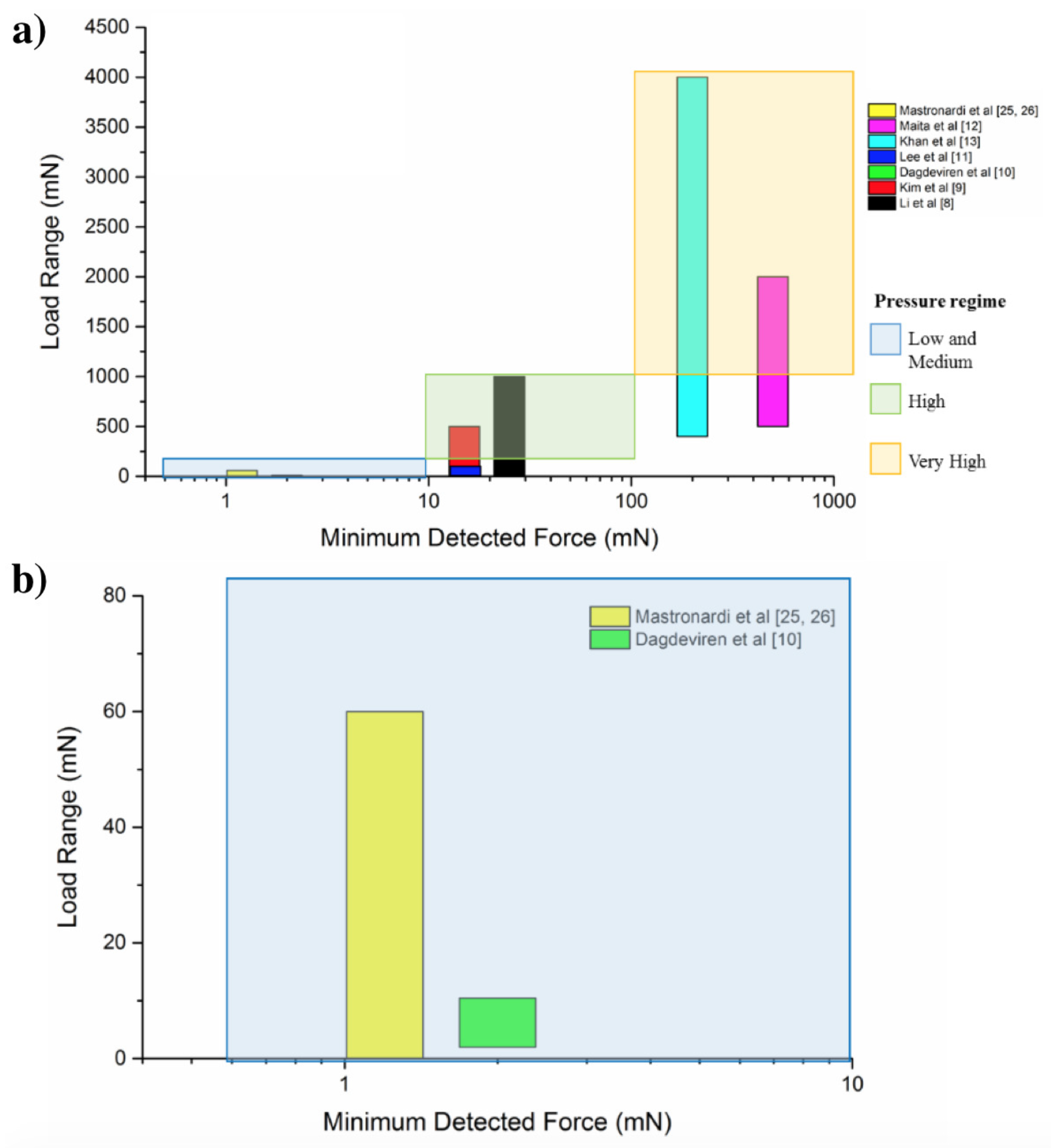
| Authors | Material | Shape | Spatial Res. a (mm) | Min. Force (mN) | Dynamic Sensitivity (mV N−1) | Static Sensitivity (fF N−1) | Load Range (mN) | Voltage Output (mV) |
|---|---|---|---|---|---|---|---|---|
| Li et al. (2008) [29] | PVDF-TrFE | Dome | 0.5 | 25 | up to 10.6 | / | 0–1000 | 0–11 |
| Kim et al. (2014) [30] | PVDF | Dome | 0.9 | 15 | up to 8830 | / | 0–500 | 0–5000 |
| Dagdeviren et al. (2014) [39] | PZT | Flat | 0.25 | 2 | 11.6 | / | 2–10.5 | 0.001–0.1 |
| Lee et al. (2014) [40] | PZT | Flat | 3 | 15.2 | 105 | / | 10–100 | 1–12 |
| Khan et al. (2015) [31] | PVDF-TrFe + MWCN | Flat | / | 200 | 500 | / | 400–4000 | 4–16 |
| Maita et al. (2014) [33] | AlN | Flat | / | 500 | 13 | / | 500–2000 | 3–10 |
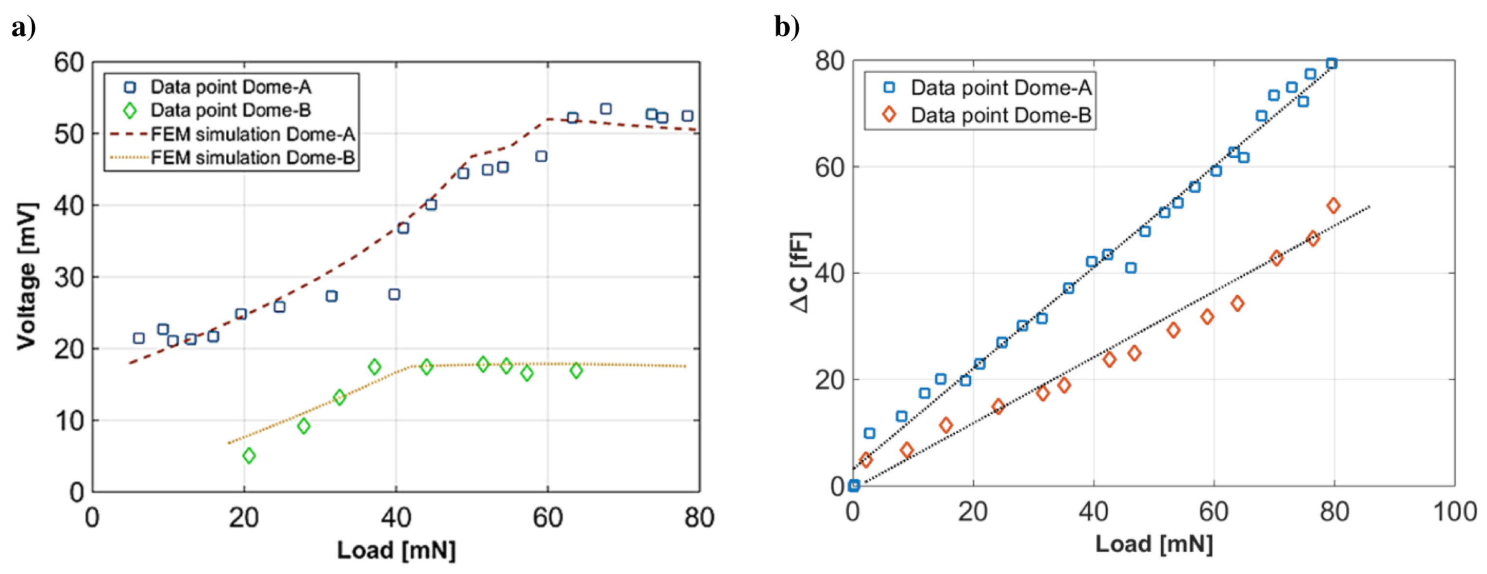
| Mastronardi et al. (2014, 2015) [27,82] | AlN | Dome | 0.75 | 1.2 | up to 480 | up to 950 | 0–60 | 0–37 |
| Authors | Material | Shape | Radius (μm) | Resonance Frequency (kHz) | Displacement (nm) | Driving Voltage (V) |
|---|---|---|---|---|---|---|
| Shelton et al. (2009) [83] | Si/SiO/AlN | Flat circular | 175–225 | 220 | 1000–1300 | 0.5–7 |
| Przybyla et al. (2010) [84] | Si/SiO/AlN | Flat circular | 200 | 214 | 100–750 | 0.5–15 |
| Akhbari et al. (2014) [77] | Si/AlN | Concave curved circular | 60–95 | 500–2190 | 0–5 | 0–10 |
| Guedes et al. (2011) [85] | Si/SiO/AlN | Flat flexurally suspended circular | 200 | 121.3 | 0–1100 | 0–30 |
| Mastronardi et al. (2014) [28] | PI/AlN | Dome curved circular | 250–300 | 390–680 | 0.5–8 | 0–10 |
© 2017 by the authors. Licensee MDPI, Basel, Switzerland. This article is an open access article distributed under the terms and conditions of the Creative Commons Attribution (CC BY) license (http://creativecommons.org/licenses/by/4.0/).
Share and Cite
Abels, C.; Mastronardi, V.M.; Guido, F.; Dattoma, T.; Qualtieri, A.; Megill, W.M.; De Vittorio, M.; Rizzi, F. Nitride-Based Materials for Flexible MEMS Tactile and Flow Sensors in Robotics. Sensors 2017, 17, 1080. https://doi.org/10.3390/s17051080
Abels C, Mastronardi VM, Guido F, Dattoma T, Qualtieri A, Megill WM, De Vittorio M, Rizzi F. Nitride-Based Materials for Flexible MEMS Tactile and Flow Sensors in Robotics. Sensors. 2017; 17(5):1080. https://doi.org/10.3390/s17051080
Chicago/Turabian StyleAbels, Claudio, Vincenzo Mariano Mastronardi, Francesco Guido, Tommaso Dattoma, Antonio Qualtieri, William M. Megill, Massimo De Vittorio, and Francesco Rizzi. 2017. "Nitride-Based Materials for Flexible MEMS Tactile and Flow Sensors in Robotics" Sensors 17, no. 5: 1080. https://doi.org/10.3390/s17051080
APA StyleAbels, C., Mastronardi, V. M., Guido, F., Dattoma, T., Qualtieri, A., Megill, W. M., De Vittorio, M., & Rizzi, F. (2017). Nitride-Based Materials for Flexible MEMS Tactile and Flow Sensors in Robotics. Sensors, 17(5), 1080. https://doi.org/10.3390/s17051080