materials-logo

Journal Browser

Journal Browser

Advances in Electronics Packaging Materials and Technology

A special issue of Materials (ISSN 1996-1944). This special issue belongs to the section "Electronic Materials".

Deadline for manuscript submissions: 20 July 2024 | Viewed by 2826

Special Issue Editor


E-Mail Website
Guest Editor
Department of Advanced Materials Engineering, Tech University of Korea, Siheung si 15073, Republic of Korea
Interests: semi-conductor & battery materials; semiconductor process; battery process; all solid state battery

Special Issue Information

Dear Colleagues,

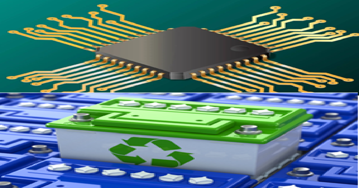
Packaging materials and technologies used in electronic products have continued to evolve with the advancement of science and technology. Electronic packaging includes various insulators, conductors, and polymer technologies to protect electronic products. With the recent emergence of mobile devices such as smartphones, packaging technology has been continuously developed to improve the reliability of manufacturing high-performance electronic products in a limited space. In the future, new technologies such as artificial intelligence, the Internet of Things, and robotics will help in developing ever more complex electronic products. Along with developing these products, electronic packaging technology is expected to develop further. Semiconductors show pattern accuracy at the 3nm level. Since high-performance semiconductor chips must be integrated into the limited space of a smartphone, related packaging technology has had to develop dramatically. In addition, in the case of secondary batteries, their use is expanding due to the rapid increase in electric vehicles. Still, higher reliability is required due to the combustion characteristics of secondary batteries, so all-solid-state batteries and high-performance packaging technologies are being actively researched. In this Special Issue, we would like to discuss the research trends of semiconductor and secondary battery reliability improvement technologies that have been actively researched recently.

Dr. Chang-Bun Yoon
Guest Editor

Manuscript Submission Information

Manuscripts should be submitted online at www.mdpi.com by registering and logging in to this website. Once you are registered, click here to go to the submission form. Manuscripts can be submitted until the deadline. All submissions that pass pre-check are peer-reviewed. Accepted papers will be published continuously in the journal (as soon as accepted) and will be listed together on the special issue website. Research articles, review articles as well as short communications are invited. For planned papers, a title and short abstract (about 100 words) can be sent to the Editorial Office for announcement on this website.

Submitted manuscripts should not have been published previously, nor be under consideration for publication elsewhere (except conference proceedings papers). All manuscripts are thoroughly refereed through a single-blind peer-review process. A guide for authors and other relevant information for submission of manuscripts is available on the Instructions for Authors page. Materials is an international peer-reviewed open access semimonthly journal published by MDPI.

Please visit the Instructions for Authors page before submitting a manuscript. The Article Processing Charge (APC) for publication in this open access journal is 2600 CHF (Swiss Francs). Submitted papers should be well formatted and use good English. Authors may use MDPI's English editing service prior to publication or during author revisions.

Keywords

  • semiconductor materials

  • battery materials
  • packaging
  • all-solid-state battery
  • reliability improvement

Published Papers (3 papers)

Order results
Result details
Select all
Export citation of selected articles as:

Research

Jump to: Review

16 pages, 2906 KiB  
Article
Cohesive Properties of Bimaterial Interfaces in Semiconductors: Experimental Study and Numerical Simulation Using an Inverse Cohesive Contact Approach
by Caio Adler, Pedro Morais, Alireza Akhavan-Safar, Ricardo J. C. Carbas, Eduardo A. S. Marques, Bala Karunamurthy and Lucas F. M. da Silva
Materials 2024, 17(2), 289; https://doi.org/10.3390/ma17020289 - 6 Jan 2024
Viewed by 859
Abstract
Examining crack propagation at the interface of bimaterial components under various conditions is essential for improving the reliability of semiconductor designs. However, the fracture behavior of bimaterial interfaces has been relatively underexplored in the literature, particularly in terms of numerical predictions. Numerical simulations [...] Read more.
Examining crack propagation at the interface of bimaterial components under various conditions is essential for improving the reliability of semiconductor designs. However, the fracture behavior of bimaterial interfaces has been relatively underexplored in the literature, particularly in terms of numerical predictions. Numerical simulations offer vital insights into the evolution of interfacial damage and stress distribution in wafers, showcasing their dependence on material properties. The lack of knowledge about specific interfaces poses a significant obstacle to the development of new products and necessitates active remediation for further progress. The objective of this paper is twofold: firstly, to experimentally investigate the behavior of bimaterial interfaces commonly found in semiconductors under quasi-static loading conditions, and secondly, to determine their respective interfacial cohesive properties using an inverse cohesive zone modeling approach. For this purpose, double cantilever beam specimens were manufactured that allow Mode I static fracture analysis of the interfaces. A compliance-based method was used to obtain the crack size during the tests and the Mode I energy release rate (GIc). Experimental results were utilized to simulate the behavior of different interfaces under specific test conditions in Abaqus. The simulation aimed to extract the interfacial cohesive contact properties of the studied bimaterial interfaces. These properties enable designers to predict the strength of the interfaces, particularly under Mode I loading conditions. To this extent, the cohesive zone modeling (CZM) assisted in defining the behavior of the damage propagation through the bimaterial interfaces. As a result, for the silicon–epoxy molding compound (EMC) interface, the results for maximum strength and GIc are, respectively, 26 MPa and 0.05 N/mm. The second interface tested consisted of polyimide and silicon oxide between the silicon and EMC layers, and the results obtained are 21.5 MPa for the maximum tensile strength and 0.02 N/mm for GIc. This study’s findings aid in predicting and mitigating failure modes in the studied chip packaging. The insights offer directions for future research, focusing on enhancing material properties and exploring the impact of manufacturing parameters and temperature conditions on delamination in multilayer semiconductors. Full article
(This article belongs to the Special Issue Advances in Electronics Packaging Materials and Technology)
Show Figures

Figure 1

12 pages, 3480 KiB  
Article
Enhancing the Plasma-Resistance Properties of Li2O–Al2O3–SiO2 Glasses for the Semiconductor Etch Process via Alkaline Earth Oxide Incorporation
by So-Won Kim, Hwan-Seok Lee, Deok-Sung Jun, Seong-Eui Lee, Joung-Ho Lee and Hee-Chul Lee
Materials 2023, 16(14), 5112; https://doi.org/10.3390/ma16145112 - 20 Jul 2023
Cited by 2 | Viewed by 1036
Abstract
To develop plasma-resistant glass materials suitable for semiconductor etching processes, we introduced alkaline earth oxides (ROs) into a Li2O–Al2O3–SiO2 (LAS) glass. Analysis of glass properties with respect to the additives revealed that among the analyzed materials, [...] Read more.
To develop plasma-resistant glass materials suitable for semiconductor etching processes, we introduced alkaline earth oxides (ROs) into a Li2O–Al2O3–SiO2 (LAS) glass. Analysis of glass properties with respect to the additives revealed that among the analyzed materials, the LAS material in which Li2O was partially replaced by MgO (MLAS) exhibited the most favorable characteristics, including a low dielectric constant (6.3) and thermal expansion coefficient (2.302 × 10⁻⁶/°C). The high performance of MLAS is attributed to the high ionic field strength of Mg2+ ions, which restricts the movement of Li+ ions under the influence of electric fields and thermal vibrations at elevated temperatures. When exposed to CF4/O2/Ar plasma, the etching speed of RO-doped glasses decreased compared with that of quartz and LAS glass, primarily owing to the generation of a high-sublimation-point fluoride layer on the surface. Herein, MLAS demonstrated the slowest etching speed, indicating exceptional plasma resistance. X-ray photoelectron spectroscopy analysis conducted immediately after plasma etching revealed that the oxidation-to-fluorination ratio of Li was the lowest for MLAS. This observation suggests that the presence of Mg2+ ions in the plasma discharge inhibits the migration of Li+ ions toward the surface, thereby contributing to the excellent plasma resistance of MLAS. Full article
(This article belongs to the Special Issue Advances in Electronics Packaging Materials and Technology)
Show Figures

Figure 1

Review

Jump to: Research

15 pages, 8369 KiB  
Review
Thermal Fatigue Failure of Micro-Solder Joints in Electronic Packaging Devices: A Review
by Lei Li, Xinyu Du, Jibing Chen and Yiping Wu
Materials 2024, 17(10), 2365; https://doi.org/10.3390/ma17102365 - 15 May 2024
Viewed by 329
Abstract
In electronic packaging products in the service process, the solder joints experience thermal fatigue due to temperature cycles, which have a significant influence on the performance of electronic products and the reliability of solder joints. In this paper, the thermal fatigue failure mechanism [...] Read more.
In electronic packaging products in the service process, the solder joints experience thermal fatigue due to temperature cycles, which have a significant influence on the performance of electronic products and the reliability of solder joints. In this paper, the thermal fatigue failure mechanism of solder joints in microelectronic packages, the microstructure changes of the thermal fatigue process, the influence factors on the joint fatigue life, and the simulation analysis and forecasting of thermal fatigue life are reviewed. The results show that the solder joints are heterogeneously coarsened, and this leads to fatigue cracks occurring under the elevated high-temperature phase of alternating temperature cycles. However, the thickness of the solder and the hold time in the high-temperature phase do not significantly influence the thermal fatigue. The coarsened region and the IMC layer thicken with the number of cycles, and the cracks initiate and propagate along the interface between the intermetallic compound (IMC) layer and coarsened region, eventually leading to solder joint failure. For lead-containing and lead-free solders, the lead-containing solder shows a faster fatigue crack growth rate and propagates by transgranular mode. Temperature and frequency affect the thermal fatigue life of solder joints to different degrees, and the fatigue lifetime of solder joints can be predicted through a variety of methods and simulated crack trajectories, but also through the use of a unified constitutive model and finite element analysis for prediction. Full article
(This article belongs to the Special Issue Advances in Electronics Packaging Materials and Technology)
Show Figures

Figure 1

Back to TopTop