materials-logo

Journal Browser

Journal Browser

Quantum Transport in Novel 2D Materials and Structures

A special issue of Materials (ISSN 1996-1944). This special issue belongs to the section "Quantum Materials".

Deadline for manuscript submissions: 20 August 2025 | Viewed by 1325

Special Issue Editor


E-Mail Website
Guest Editor
Department of Condensed Matter Theory and Nanophysics, Jagiellonian University, Kraków, Poland
Interests: graphene; quantum entanglement; superconductivity; condensed matter theory; 2D materials
Special Issues, Collections and Topics in MDPI journals

Special Issue Information

Dear Colleagues,

The advent of semiconducting heterostructures in the 1980s allowed researchers to demonstrate—in real world—several surprising phenomena described by theorists (at least to some degree) decades earlier, including the conductance quantization, quantum Hall effect, and Aharonov–Bohm effect.

The discovery of graphene and other truly two-dimensional (i.e., atomically thin) crystals, and the subsequent fabrication of nanostructures containing these materials, has not only made it possible to study the above phenomena more precisely but has also led to the discovery of entirely new physical effects, at least in the world of condensed matter, related to chirality, transmission via evanescent waves, or additional degrees of freedom (valleys) characterizing the effective Dirac quasiparticles. In addition, ambipolar doping, gate-controlled energy gap, mechanical flexibility, and the effects of deformation on the electronic structure allow for the design of electronic (or electromechanical) devices that have no analogues in silicon-based electronics.

In addition, in the field of 2D materials, there have been several significant recent discoveries. Firstly, the observation of unconventional quantum Hall effects in 2D materials is remarkable. This includes phenomena such as quantized Hall resistance and fractional quantum Hall effects. These findings have deepened our understanding of the quantum behavior in these materials. Secondly, the emergence of topological phases in 2D materials is an important advancement. For example, the discovery of the quantum spin Hall effect in monolayer graphene and transition metal dichalcogenides (TMDs) has opened up new research directions. It indicates the presence of unique topological properties in these 2D systems. Thirdly, the study of quantum transport in van der Waals heterostructures is a growing area of interest. When different 2D materials are stacked with precise atomic arrangement control, interesting phenomena occur. Examples include moiré superlattices that can modulate electronic properties and the correlated electron behavior that emerges due to strong electron–electron interactions. This research offers insights into the transport properties and potential applications of these complex 2D material structures. Overall, these recent discoveries in 2D materials have broadened our knowledge and hold great potential for various technological applications in the future.

This Special Issue aims to present a collection of research articles covering different aspects of charge, spin or energy transport in two-dimensional materials, or more complex structures containing these materials, from the analysis of physical principles to computer simulations and experiments.

We hope that the prospective set of results will both shed light on fundamental aspects of the phenomena under consideration and stimulate more practical device development.

Prof. Dr. Adam Rycerz
Guest Editor

Manuscript Submission Information

Manuscripts should be submitted online at www.mdpi.com by registering and logging in to this website. Once you are registered, click here to go to the submission form. Manuscripts can be submitted until the deadline. All submissions that pass pre-check are peer-reviewed. Accepted papers will be published continuously in the journal (as soon as accepted) and will be listed together on the special issue website. Research articles, review articles as well as short communications are invited. For planned papers, a title and short abstract (about 100 words) can be sent to the Editorial Office for announcement on this website.

Submitted manuscripts should not have been published previously, nor be under consideration for publication elsewhere (except conference proceedings papers). All manuscripts are thoroughly refereed through a single-blind peer-review process. A guide for authors and other relevant information for submission of manuscripts is available on the Instructions for Authors page. Materials is an international peer-reviewed open access semimonthly journal published by MDPI.

Please visit the Instructions for Authors page before submitting a manuscript. The Article Processing Charge (APC) for publication in this open access journal is 2600 CHF (Swiss Francs). Submitted papers should be well formatted and use good English. Authors may use MDPI's English editing service prior to publication or during author revisions.

Keywords

  • graphene
  • silicene
  • germanene
  • transition metal dichalcogenides
  • 2D materials
  • spintronics
  • valleytronics
  • nanotubes
  • quantum transport
  • Landauer–Buttiker formalism

Benefits of Publishing in a Special Issue

  • Ease of navigation: Grouping papers by topic helps scholars navigate broad scope journals more efficiently.
  • Greater discoverability: Special Issues support the reach and impact of scientific research. Articles in Special Issues are more discoverable and cited more frequently.
  • Expansion of research network: Special Issues facilitate connections among authors, fostering scientific collaborations.
  • External promotion: Articles in Special Issues are often promoted through the journal's social media, increasing their visibility.
  • e-Book format: Special Issues with more than 10 articles can be published as dedicated e-books, ensuring wide and rapid dissemination.

Further information on MDPI's Special Issue policies can be found here.

Published Papers (3 papers)

Order results
Result details
Select all
Export citation of selected articles as:

Research

35 pages, 5269 KiB  
Article
The Quantum Transport of Dirac Fermions in Selected Graphene Nanosystems Away from the Charge Neutrality Point
by Adam Rycerz
Materials 2025, 18(9), 2036; https://doi.org/10.3390/ma18092036 - 29 Apr 2025
Abstract
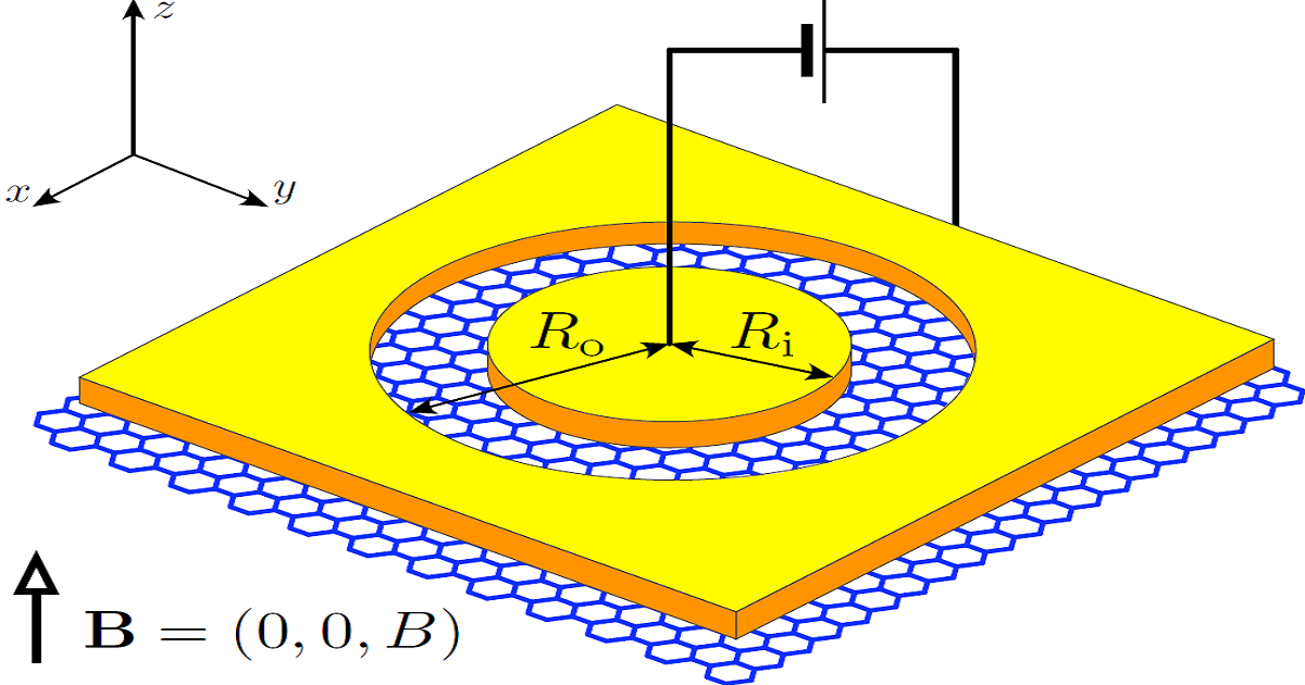
The peculiar electronic properties of graphene, including the universal dc conductivity and the pseudodiffusive shot noise, are usually found in a small vicinity close to the charge neutrality point, away from which the electron’s effective mass raises, and nanostructures in graphene start to [...] Read more.
The peculiar electronic properties of graphene, including the universal dc conductivity and the pseudodiffusive shot noise, are usually found in a small vicinity close to the charge neutrality point, away from which the electron’s effective mass raises, and nanostructures in graphene start to behave similarly to familiar Sharvin contacts in semiconducting heterostructures. Recently, it was pointed out that as long as abrupt potential steps separate the sample area from the leads, some graphene-specific features can be identified relatively far from the charge neutrality point. These features include greater conductance reduction and shot noise enhancement compared to the standard Sharvin values. The purpose of this paper is twofold: First, we extend the previous analysis based on the effective Dirac equation, and derive the formulas that allow the calculation of the arbitrary charge transfer cumulant for doped graphene. Second, the results of the analytic considerations are compared with numerical simulations of quantum transport on the honeycomb lattice for selected nanosystems for which considerations starting from the Dirac equation cannot be directly adapted. For a wedge-shaped constriction with zigzag edges, the transport characteristics can be tuned from graphene-specific (sub-Sharvin) values to standard Sharvin values by varying the electrostatic potential profile in the narrowest section. A similar scenario is followed by the half-Corbino disk. In contrast, a circular quantum dot with two narrow openings showing a mixed behavior appears: the conductance is close to the Sharvin value, while the Fano factor approaches the value characterizing the symmetric chaotic cavity. Carving a hole in the quantum dot to eliminate direct trajectories between the openings reduces the conductance to sub-Sharvin value, but the Fano factor is unaffected. Our results suggest that experimental attempts to verify the predictions for the sub-Sharvin transport regime should focus on systems with relatively wide openings, where the scattering at the sample edges is insignificant next to the scattering at the sample–lead interfaces. Full article
(This article belongs to the Special Issue Quantum Transport in Novel 2D Materials and Structures)
Show Figures

Figure 1

10 pages, 3175 KiB  
Article
Electric Field-Defined Superlattices in Bilayer Graphene: Formation of Topological Bands in Two Dimensions
by Włodzimierz Jaskólski
Materials 2025, 18(7), 1521; https://doi.org/10.3390/ma18071521 - 28 Mar 2025
Viewed by 313
Abstract
An electric field applied to the Bernal-stacked bilayer graphene opens an energy gap; its reversal in some regions creates domain walls and leads to the appearance of one-dimensional chiral gapless states localized at the walls. Here, we investigate the energy structure of bilayer [...] Read more.
An electric field applied to the Bernal-stacked bilayer graphene opens an energy gap; its reversal in some regions creates domain walls and leads to the appearance of one-dimensional chiral gapless states localized at the walls. Here, we investigate the energy structure of bilayer graphene with superlattice potential defined by an external electric field. The calculations are performed within an atomistic π-electron tight-binding approximation. We study one-dimensional and two-dimensional superlattices formed by arrays of electric-field walls in the zigzag and armchair directions and investigate different field polarizations. Chiral gapless states discretize due to the superlattice potential and transform into minibands in the energy gap. As the main result, we show that the minibands can cross at the Fermi level for some field polarizations. This leads to a new kind of two-dimensional gapless states of topological character that form Dirac-like cones at the crossing points. This also has application potential: changing the field polarization can close the energy gap and change the character of the superlattice from semiconducting to metallic. Full article
(This article belongs to the Special Issue Quantum Transport in Novel 2D Materials and Structures)
Show Figures

Figure 1

18 pages, 5371 KiB  
Article
Resonant and Non-Resonant Impurity States Related to GaAs/AlGaAs Quantum Well Sub-Bands
by Volodymyr Akimov, Viktor Tulupenko, Roman Demediuk, Anton Tiutiunnyk, Carlos A. Duque, Alvaro L. Morales, David Laroze and Miguel Eduardo Mora-Ramos
Materials 2025, 18(1), 17; https://doi.org/10.3390/ma18010017 - 24 Dec 2024
Viewed by 695
Abstract
The energy positions and wave function shapes of the ground and excited states of impurities, including resonance states, are studied using the expansion of the impurity wave function in basis functions. The structures under study are rectangular GaAs/AlGaAs quantum wells with four different [...] Read more.
The energy positions and wave function shapes of the ground and excited states of impurities, including resonance states, are studied using the expansion of the impurity wave function in basis functions. The structures under study are rectangular GaAs/AlGaAs quantum wells with four different widths. In all cases, the impurity binding energy (relative to the corresponding sub-band) has a maximum at or near the center of the quantum well, decreases as the heterointerface is approached, and apparently has a limit of 0 if the impurity moves deeper into the barrier. If the impurity moves away from the center of the quantum well, then the “center of mass” of the electron charge of non-resonant impurity states follows the impurity atom, and the “center of mass” of the electron charge of the resonant impurity states moves away from it. The effect is more pronounced for the ground and first resonance states for wider quantum wells, and the shifts reach a maximum when the impurity atom is positioned near the midpoint of the path between the quantum well center and the heterointerface. Full article
(This article belongs to the Special Issue Quantum Transport in Novel 2D Materials and Structures)
Show Figures

Figure 1

Back to TopTop