Abstract
Polarization volume gratings (PVGs) have been recognized as a groundbreaking technology with the potential to revolutionize holographic waveguides and facilitate immersive experiences in augmented and virtual reality (AR/VR) applications. This study investigated the design, fabrication, and utilization of PVGs within the framework of holographic waveguides for immersive encounters. The essay begins by presenting a comprehensive overview of waveguide technologies. The display devices and optical combiners combine the actual and virtual worlds that the naked eye can see. This review categorizes current visual solutions for micro-optical combiners in augmented reality head-mounted displays (AR-HMDs). Subsequently, an investigation was carried out into the manufacturing process, physical principles, optical structures, performance characteristics, and other aspects. Furthermore, a review and assessment of their merits and drawbacks were conducted.
1. Introduction
The rapid growth in AR/VR technologies in recent years has transformed the way we view and interact with digital content. The potential of AR and VR technologies to transform various domains from entertainment and gaming to education, healthcare, and industrial applications has gained significant attention [1,2,3,4,5]. The key to unlocking the true potential of AR and VR lies in developing advanced waveguide technologies that seamlessly deliver immersive and realistic experiences to users. AR displays virtual objects on real-world objects using optical combiners and display devices. One often-employed method involves using transparent optical components, facilitating the concurrent perception of virtual and actual pictures by the human visual system [6,7].
Traditionally, waveguides have played a critical role in directing and delivering visual information to the user’s eyes. However, their weight, size, and field-of-view (FOV) limitations have hindered their widespread application. However, pursuing more immersive and realistic AR/VR experiences has driven academics to seek unique solutions. The introduction of PVGs as a holographic waveguide solution offers a promising approach to overcome these limitations and paves the way for enhanced immersive experiences [8]. PVGs that exhibit excellent efficiency, wide diffraction angle, efficient waveguide coupling, straightforward fabrication procedure, and exceptional polarization selectivity offer valuable insights into distinctive molecule orientation profiles as a subset of Bragg gratings [9]. One can achieve a functioning planar device with a programmed optical axis orientation using many approaches, including the use of reflecting PVGs made of liquid crystals (LC), the utilization of a linear Bragg-Berry phase optical element, or the incorporation of a component consisting of volume Bragg gratings (VBGs). Patterned cholesteric liquid crystals (CLC) are becoming increasingly popular in LC research and photonics. PVG structures offer significant benefits for the development of cutting-edge optical devices and displays, particularly near-eye optical systems. This can be attributed to their intriguing fabrication processes and distinctive visual characteristics [8]. Unlike traditional Bragg gratings, such as volume holographic gratings (VHGs), PVGs attain an almost perfect diffraction efficiency at a far higher diffraction angle and demonstrate a more noticeable sensitivity to the angle of incoming light. PVGs have attractive attributes, including flexibility, thermal conductivity, electrical responsiveness, and other similar properties [9,10].
O. Lavrentovich, and F. Simoni et al. [9,10,11,12,13,14,15] have made notable contributions in LC technology, particularly through their exploration of electrically and optically tunable Bragg reflection in oblique helicoidal cholesterics. Their groundbreaking work demonstrated how electric fields can precisely tune light reflection across an extensive spectrum by altering the pitch and orientation of heliconical cholesteric structures. This novel ability is further illustrated through their research on twist-bend nematic phases and cholesteric gratings, revealing the unique optical characteristics that emerge from the heliconical configuration. These advancements in selective reflection and laser technology are significant milestones in the development of advanced materials for photonics and display technologies. Their innovative approach to constructing responsive and adaptive optical interfaces integrates dynamic LC technologies into AR and VR systems, setting the stage for unprecedented levels of control and versatility in visual technology [16,17,18,19,20,21,22].
The research conducted by Qi-Huo Wei et al. [23,24,25] on photopatterned optical elements delves into the innovative use of plasmonic meta masks and photoalignment techniques to precisely control the molecular orientations in LCs. Their work on the patterning of lyotropic chromonic LCs with photonic metamasks demonstrated the ability to achieve exact molecular alignment through photopatterning, leading to the development of advanced optical elements with complex molecular arrangements. By leveraging high-resolution, high-throughput plasmonic photopatterning, the team has introduced new approaches for crafting structured LC systems that serve as tunable optical devices. This research has significant potential for advancing responsive and dynamic photonic materials, with profound implications for the fields of advanced displays, sensors, and other optoelectronic applications [26].
Sato et al. [27,28] have made significant advancements in the development of LC lenses with electrically controlled focal lengths. Their research has concentrated on creating lenses capable of dynamically adjusting their focal length over a wide range by integrating LC layers with traditional glass lenses. This innovation facilitates the precise control of optical properties through electric fields, enabling applications in adaptive optics, imaging systems, and augmented reality (AR) devices.
Jakli et al. [29,30,31,32,33,34,35,36] have made profound contributions to the field of LC technologies, spanning a wide range of innovations. Their work includes the development of electromagnetic and ferroelectric nematic LCs that undergo vitrification at room temperature, a breakthrough with significant implications for high-performance displays. In addition, they pioneered electrically tunable chiral LC lenses and microlenses incorporating Pancharatnam-Berry phases, which are poised to enhance the optical devices used in AR and VR systems [37]. Their research on LC elastomers and the precise control of molecular orientations in these materials further propels the advancement of adaptive optics and responsive interfaces, enabling more immersive and versatile AR/VR experiences [33,38,39,40,41].
Shin Tsin Wu et al. [42,43,44,45,46,47] have made notable advancements in AR and VR displays, focusing on improving optical efficiency, enhancing image quality, and addressing challenges associated with current display technologies. Their research encompasses waveguide-based AR displays, PVGs, and liquid-crystal-on-silicon (LCoS) for AR. Notably, their work on surpassing the in-coupling efficiency limit with PVGs, developing high-efficiency pancake optics, and optimizing the microdisplay requirements for VR has been pivotal in advancing AR/VR display technologies [2,43,48,49].
Kristiaan Neyts et al. [50,51,52,53,54] have significantly contributed to the development of LC technologies, particularly in photonic devices and advanced optical applications. Their investigation into multidomain LC structures and Pancharatnam–Berry phase gratings has been crucial for enhancing the efficiency and compactness of beam combiners, which are vital for next-generation AR and VR interfaces. Their work bridges the gap between fundamental LC physics and practical photonic devices, offering innovative solutions for high-performance AR/VR displays.
This study analyzes the latest developments in LC-based PVGs and introduces innovative devices and systems that utilize this intriguing optical component.
2. Classification
Optical phenomena are classified into three main groups: macro-optical, micro-optical, and nano-optical. This classification is primarily based on the size scale of the optical systems or phenomena, which determines the optical principles and methods applied. Macro-optical systems involve components that are much larger than the wavelength of light (typically greater than 1 mm), where classical geometric optics such as reflection, refraction, and diffraction are used. Micro-optical systems, with components ranging from 1 µm to 100 µm, experience significant diffraction and interference effects, requiring more complex treatments that go beyond ray optics, such as in micro-lenses and waveguides. Nano-optical systems operate at the nanometer scale (typically less than 100 nm), where quantum effects dominate, and light interacts strongly with nanostructured materials, leading to phenomena such as plasmonic and subwavelength focusing. This classification helps to distinguish optical systems based on their scale and the corresponding physical principles that govern their behavior.
Categorizing AR-HMDs based on optical design poses significant challenges. The performance evaluation of AR-HMD in visual design often involves assessing several vital aspects, including FOV, transmittance, modulation transfer function (MTF), eye box, light effectiveness, and mass [55,56]. Initially, mainstream AR-HMDs utilized optical designs that relied on a combination of reflective and refractive lens elements. This approach aims to provide eyes with high-brightness images. Initial attempts were impeded by the constraints of the processing technology and design methodologies, which ultimately resulted in the implementation of simple rotationally symmetric coaxial optical imaging systems. Nevertheless, these methods must meet growing requirements, such as a substantial FOV, superior resolution, and slender configurations [57,58,59].
Progress in processing technologies, design methodologies, and surface description techniques has enabled the formation of reflective and off-axis refractive structures, which are constructed using freeform surfaces (FFS) and aspheric surfaces (AS). As previously stated, this has led to the creation of multiple catadioptric AR-HMD platforms. Aberrations in optical imaging systems can be effectively corrected by utilizing Adaptive Optics Systems (AOS) and Fast Fourier Transform (FFT) [60,61]. In addition to increasing the FOV and attaining a high resolution, it is possible to represent a structure that is lightweight and compact [62]. Progress in high-precision optical injection processing technologies has facilitated the effective mass production of aspheric and freeform optical lenses. In recent years, AR-HMDs that use advanced optics such AS and FFS technologies have emerged as primary devices capable of meeting the demands of commercial manufacturing [63,64].
AR-HMDs that utilize geometric optical waveguides have the potential to offer more compact and lightweight systems, thus exhibiting characteristics similar to those of prescription glasses. However, some notable obstacles and complexities have emerged regarding the consistency of illumination, suppression of stray light, and FOV enlargement. Furthermore, the attainment of mass production poses challenges because of the intricate nature of their processing technologies. One of the challenges associated with optical invariants is their limitations, and particularly their applicability. Specifically, using optical invariants poses difficulties in the optical domain [65,66].
The utilization of diffractive optical elements (DOE) in AR-HMD systems has attracted considerable attention. When a light beam is incident at a specific angle, the occurrence of DOE leads to a greater deviation angle of the beam compared with the influences of geometric refraction and reflection. In 1996, researchers utilized DOEs AR-HMDs to reduce the overall weight and optical aberrations of a device. After more than ten-year-long development, a diffraction waveguide AR-HMD was successfully fabricated for surface relief grating (SRG) waveguides and VHG waveguides. The developed AR-HMD is distinguished by its slim and lightweight waveguide design, which represents the anticipated form of the future AR-HMDs. Research on planar diffractive waveguide technology has attracted considerable attention because of its advantageous properties in terms of the form factor and substantial effective propagation distance (EPD). AR-HMDs in consumer electronics have emerged as prominent research areas and have attracted significant attention [67,68,69,70].
Nevertheless, the existing diffraction waveguide AR-HMD continue to face certain limitations that impede their widespread use in commercial settings. Some of these problems include low efficiency, chromatic distortion in full-color displays, uneven illuminance, and a scarcity of mass-production processing methods [60,61,71].
Significant research and development efforts have been devoted to studying LC-based gratings and PVG structures. PVGs are made from an LC film, which allows it to achieve a light diffraction efficiency close to 100%. Researchers have focused on the employment of metalenses in AR-HMDs owing to their exceptional abilities in wavefront phase adjustment and geometric features of flat components [72,73].
Figure 1 shows the current AR-HMD optical combiner solutions, which can be split into three main groups: macro-, micro-, and nano-optical. Macro-visual solutions encompass a range of methodologies, including traditional visual methods, free-form prism techniques, and geometric optical waveguide solutions [63]. These methods are based on Snell’s law, which regulates the bending and bouncing of light. Micro-optical solutions comprise many diffraction grating optical solutions, including SRGs, VHGs, and PVGs, which pertain to light deflection phenomena resulting from grating diffraction. Nano-optical solutions encompass metalenses and metasurface reflector solutions, which rely on manipulating phase modulation effects inside nanoscale microstructures [74].
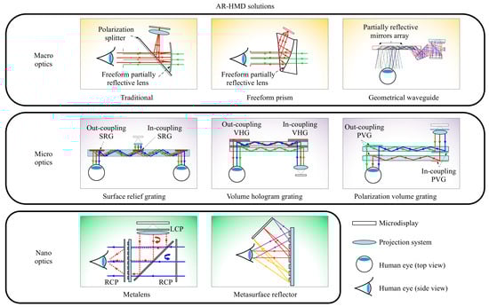
Figure 1.
Fundamental classification of AR-HMD optical solutions, adapted from ref. [63] with permission from the Light: Advanced Manufacturing.
This study comprehensively examines the categorization of AR-HMD micro-optics optical solutions, followed by an analysis of the latest developments in LC-based PVGs. The investigation starts by configuring the LC director to clarify the operational principles of PVGs. In the subsequent section, an examination of the theoretical model is presented, wherein the distinctive optical properties are explained based on the simulation results. The next section focuses on the fabrication process and applications of PVGs.
2.1. Micro-Optical Solutions
In micro-optical solutions, the categorization of planar diffractive waveguides is based on their various periodic structural forms, resulting in three main types: SRG, VHG, and PVG waveguides. The subsequent sections analyze the efficiency of three distinct varieties of grating waveguides.
2.1.1. SRG Waveguide
An SRG waveguide is commonly incorporated into the display module of the headset in an HMD-AR system. It comprises a thin transparent substrate with a patterned surface relief structure. This structure acts as a diffraction grating, manipulating and guiding light from the display source toward the user’s eyes, allowing it to exit the waveguide and be perceived as a virtual image. The structure is typically engineered to achieve a specific diffraction angle and distribution of diffracted light, ensuring an accurate and immersive visual presentation [75].
The operation of the SRG waveguide is based on the concept of total internal reflection (TIR). When light is incident on the waveguide originating from the display source, it experiences TIR at the contact between the waveguide substrate and the surrounding medium. This TIR phenomenon ensures that the light is trapped within the waveguide and propagates along its length. One of their advantages is the ability of SRG waveguides in AR-HMD systems to provide a wide FOV while maintaining compact form factors. Through rigorous surface relief structure design and rigorous optimization of waveguide parameters, it is feasible to obtain an AR experience with a wide FOV while maintaining the compactness and lightweight nature of the headset [76,77].
Figure 2a illustrates the essential elements of a standard one-dimensional binary rectangular grating, including the period, groove dimensions, and duty cycle. NOKIA63 pioneered the initial application of a binary rectangular grating that served as a binocular VR display. Diffraction occurs when the collimated beam interacts with the in-coupling grating, causing the beam to propagate in two symmetric directions by TIR, as shown in Figure 2b. The left and right eyes eventually detect the light as it emerges from the outcoupling grating [78]. The use of an inclined SRG causes a departure from the inherent symmetry of the grating, resulting in a notable increase in the diffraction efficiency within a specific order. Figure 2c depicts a frequently employed slanted surface-relief grating, in which the binary rectangular grating groove is inclined at a specific angle away from the perpendicular line. During the design phase, it is imperative to determine the duty cycle, tilt angle, and groove depth in addition to the grating period. Maintaining a precise distance between the eye and the observed item is crucial during application. Enlarging the exit pupil at the exit-coupling terminal is essential for optimizing the visual perception of the entire image while moving along the direction of light propagation within the waveguide. Successful attainment of exit pupil expansion (EPE) requires accurate fabrication of the outcoupling diffraction grating components, as shown in Figure 2d [79,80].
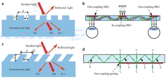
Figure 2.
Waveguide and 1D grating structure: (a) rectangular grating structure, the arrows indicate incident light (approaching the surface), reflected light (rebounding from the surface), and transmitted light (passing through the material), with diffraction orders (D1, D0, D-1) showing how the light splits due to the grating. (b) binocular diffraction waveguide structure, and the arrows illustrate the diffraction and coupling of light through in-coupling and out-coupling SRG, with colored arrows corresponding to different diffraction orders. (c) tilted grating structure, and similar light interactions with a grating, with diffraction orders labeled as D1, D0, and D-1 (d) a 1D pupil expansion structure, and arrows represent the intensities of incident (I0, I1, I2, I3), reflected (r1, r2, r3), and transmitted light (t1, t2, t3) at different angles, demonstrating how light is reflected, transmitted, and diffracted by the optical components. reproduced from Ref. [63] with permission from Light: Advanced Manufacturing.
To provide a complete and accurate representation of colors, it is necessary to use a single-layer diffractive waveguide to ensure that the TIR of red, green, and blue (RGB) light occurs within an acceptable range. However, it is essential to recognize that the FOV for red light is restricted to a narrow wavelength range. To achieve a thorough color display, it is essential to explore other approaches to enlarge the FOV of the color waveguide [81]. A practical approach to accomplish this objective is to employ grating waveguides with varying periods to capture a wide range of light waves, thereby enhancing the FOV of the waveguide. The utilization of a two-layer waveguide stack arrangement was implemented by the Nokia Research Center, as illustrated in Figure 3a from the Nokia Research Center.
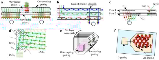
Figure 3.
Two-dimensional (2D) EPE and a stack structure consisting of many layers of waveguides. (a) Construction of a waveguide stack consisting of two layers and the arrows show light traveling through waveguide guides and interacting with the out-coupling grating; (b) construction of a color waveguide with three layers, representing the RGB color model and illustrates diffraction through a slanted grating with light paths corresponding to different wavelengths (blue, green, red).; (c) working principle of a one-dimensional EPE that provides a wide FOV and arrows depict light rays passing through optical plates and being diffracted by gratings G1 and G2; (d) schematic representation of a two-dimensional EPE and shows light interacting with diffractive optical elements (DOEs) in a waveguide, with arrows indicating the light’s modified directions; (e) superposition of six layers of an SRG waveguide to produce several focus planes highlights light propagation through a six-layer waveguide system with in-coupling and out-coupling gratings; (f) pupil enlargement employing a 2-D grating SRG waveguide [63] with permission from Light: Advanced Manufacturing.
The lower plate had a shorter grating period than the upper plate. This configuration entails the utilization of a single layer dedicated to red wavelengths, whereas the other layer is dedicated to blue and green wavelengths. Figure 3b shows the waveguide stack configuration in Microsoft HoloLens, which encompasses three distinct layers [6,82,83].
An alternative approach involves segmenting an EPE function into two distinct components. The two plates shielded the positive and negative incident angles, respectively. This can be accomplished by choosing different grating periods, as illustrated in Figure 3c. Scholars have proposed a method for enhancing the size of the eyebox by utilizing a 2-D EPE structure, as depicted in Figure 3d. A redirection grating, specifically DOE2, is necessary to implement 2D EPE systems. As the light beam propagates towards DOE2, it undergoes constant interaction with DOE2, resulting in a transformation from 1D propagation to 2D beam propagation. According to the illustration, the vertical expansion of the beam is observed before it arrives at DOE3. Following the DOE3 diffraction process, it can be observed that expansion of the horizontal direction occurs, ultimately resulting in the formation of a 2D beam band. The diffractive waveguides manufactured by Microsoft and Digi Lens were found to have a 2D-EPE structure. The first version of the HoloLens system incorporated an optical module with a three-layer waveguide stack architecture to support RGB light. This module provides a 35° diagonal FOV. The second-generation optical module had a two-layer waveguide stack with a 50° diagonal FOV. Compared to its predecessor, the second-generation FOV has improved substantially [6,84].
The focus signals provided by virtual scenes in these near-eye display technologies are insufficient for the human eye. As depicted in Figure 3e, Magic Leap devised a solution to mitigate the issue of the vergence-accommodation conflict (VAC) by employing a configuration consisting of six SRG waveguides. Each waveguide was allocated to a distinct color wavelength RBG to generate multiple focal planes. Among these layers, three are responsible for providing near-focus vision, whereas the remaining three are responsible for rendering the focused content at a distance. Subsequently, these images are allocated to two distinct focus planes, enhancing the visual comfort experienced by human observers [85]. Two-dimensional gratings can achieve the same functionality as planar waveguides, in addition to one-dimensional grating waveguides. The subwavelength grating structure displays unique periodic patterns along two mutually perpendicular directions. A 2D grating, as illustrated in Figure 3f, was employed to meet the 2D EPE criterion. This grating uses pupil duplication in two perpendicular directions. Wave-optic optical waveguide display technology has been implemented in several contexts [86,87]. There are still issues that need to be solved that hinder the broader implementation of SRG. Diffraction waveguides exhibit significant angular and wavelength selectivity in their design. However, they are susceptible to dispersion issues that can lead to a non-uniform color distribution within the exit pupil, generating a rainbow-like phenomenon. Additionally, it is essential to consider the presence of higher diffraction orders in the diffraction gratings. These higher-order diffracted lights may result in a phenomenon known as light leakage, in which light escapes outside the confines of the optical waveguide. When considering the processing technology for the manufacture of SRG, it is essential to prevent the use of extensive angles for the grating slant [88].
Furthermore, the line-to-depth ratio should be manageable. The excessive length of a structure may be an issue in the context of the nanoimprint stage because of the restrictions imposed by Young’s modulus, potentially impairing its capacity to maintain its desired shape. The consequence of this action is the immediate breakdown of the impression grating. Acquiring EBL exposure apparatuses, essential for tool manufacturing, necessitates significant financial investment owing to their high cost. Furthermore, these instruments require a specific ultra-clean environment for reliable precision and efficient operation [89,90,91].
2.1.2. VHG Waveguide
The VHG waveguide system is an alternative approach to light waveguides. The VHG is an architectural structure in three dimensions that is distinguished by a repetitive refractive index created using the interference principle. Under ideal circumstances, the diffraction efficiency approaches 100% when the Bragg condition is satisfied. A decrease in the diffraction efficiency is evident when the departure angle increases to 80 °. VHG can be categorized into two main classifications: reflective and transmissive. The utilization of reflection volume holograms is widespread in waveguides [92]. The coupled wave theory was introduced by Kognik et al. as a method for analyzing the diffraction characteristics of VHG [93]. The concept of employing holographic diffractive elements for HMD was introduced by Amitai et al. [94]. Since 2007, BAE Systems, a prominent British firm, has been committed to exploring and advancing the Q-sight range of waveguide products [95]. In pursuit of these objectives, transmissive holographic gratings have been incorporated into HMDs designs.
When the incident light undergoes TIR within the glass substrate, it subsequently undergoes diffraction upon encountering a holographic surface. Light that has undergone diffraction no longer meets the requirements for TIR and is consequently emitted from the glass plate. Furthermore, it is possible to modify the size of the entrance pupil to maintain a consistent light-departure region, as depicted in Figure 4a [95,96]. Sony created a full-color waveguide display in 2008 using a technique known as multiple holographic layer superposition [63]. Volume hologram stacks for in-coupling and out-coupling reflections were used in the waveguide. Nevertheless, the presence of many holographic layer superpositions might give rise to the issue of stray light owing to the inherent variability in the gratings of each hologram layer. Consequently, the optical axes of the display and collimator are inclined at an angle of 10° with respect to the hologram, as shown in Figure 4b. As a result, the Bragg wavelength parallax observed between the two extremities of the FOV decreased from 45 to 37 nm, but the color range increased from 76% to 120%. In 2015, a dual-sided HOE was created with a slight deviation from the ideal mirror-striped design, as shown in Figure 4c. Consequently, achieving a luminosity three times greater while maintaining uniformity is possible, resulting in an expanded FOV of approximately 19 × 6. Consumers express satisfaction not only in the absence of chromatic aberration and the regularity of images, but also with their desire to acquire AR goods that are lightweight and compact [97,98,99].
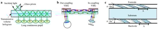
Figure 4.
(a) The holographic optical waveguide was optimized by BAE Systems (one-axis displayed) and the arrows show the incident light entering the glass prism and passing through the transmissive volume hologram, which deflects and directs the light through the long continuous pupil., (b) The full-color schematic of a VHG waveguide with an oblique optical axis by Sony. The arrows represent light diffracting at the out-coupling and in-coupling VHGs, with different colored arrows corresponding to distinct diffraction orders (red, green, blue). The arrows demonstrate how light is coupled in and out of the system via the gratings, (c) The schematic of a VHG waveguide with a deviation mirror-striped structure by Sony, the arrows indicate the direction of light as it passes through the frontside and backside of the material, with periodic features (Λ) on both sides controlling the diffraction properties modified from ref. [63] with permission from Light: Advanced Manufacturing.
When comparing VHG waveguides to SRG and geometric waveguides, it is observed that VHG waveguides exhibit reduced research and developmental expenses as well as accelerated production processes. The manufacturing of VHG waveguides faces numerous obstacles, including the fabrication of holographic materials. Presently, most producers utilize photopolymer materials as media. It is important to recognize that these materials have unique characteristics that directly affect the evenness of the coating, the FOV of the waveguide, and other optical features. Moreover, the environmental stability requirements for the exposure and production processes of holographic waveguides are extremely stringent. Humidity, temperature, and air circulation have an impact on exposure. Furthermore, owing to the inherent constraints of holographic waveguide technology, expanding the FOV of holographic waveguides becomes challenging [100,101].
The primary objectives are to investigate the potential of PVGs in advancing optical systems, with a particular emphasis on their applications in AR and VR. The study aims to explore how these technologies can enhance the manipulation of light, improving system performance and efficiency. Specifically, this paper pursues to optimize the quality of visual experiences, interactivity, and immersion in AR/VR environments by integrating PVGs, thereby pushing the boundaries of display technologies. Another key objective is to propose and design novel optical devices that leverage these components, offering more compact, efficient, and scalable solutions for a range of applications, including optical sensing, imaging, and holography. By addressing these objectives, the paper aims to contribute to the development of next-generation optical systems and technologies, paving the way for more immersive and high-performance AR/VR applications.
2.1.3. PVGs Waveguide
Patterned CLC are increasingly used in the fields of LC and photonics, leading to the growing popularity of PVGs. PVGs have demonstrated significant benefits in emerging optical devices and upcoming displays, particularly near-eye optical systems. This can be attributed to the intriguing manufacturing procedures and distinctive optical characteristics of these materials.
Pancharatnam-Berry phase optical elements (PBOEs) have emerged as novel optical components on the LC front that resemble cycloidal diffractive wave plates (CDWs). Various practical optical effects have been accomplished utilizing PBOEs, including but not limited to focusing, wavelength selection, and waveguide coupling [102,103].
PBOEs possess notable optical tunability, polarization selectivity, and diffraction efficiency characteristics, making them highly promising for many applications in future display systems. When VHG and CDW are compared, the CDW has polarization sensitivity, resulting in a considerable increase in the diffraction efficiency. When the polarization handedness of the incident beam is properly aligned [104]. However, owing to the limitations imposed by physical factors, the diffraction angle of CDW tends to remain relatively small, often measuring approximately 15° when observed in an atmospheric environment. PVGs is a recently introduced material that has been suggested to combine the advantages of VHG with CDWs, possessing a reduced thickness compared to traditional VHG by a few tens of microns [105].
Compared to VHG, which displays a refractive index modulation of approximately 10−2, PVGs exhibit a significantly stronger modulation, with a predominant value of 0.2. Theoretically, it is feasible to achieve any desired diffraction angle by adjusting the size of the period. Achieving any desired diffraction angle is feasible by adjusting the period’s size along the x- and y-axes. The dependence of the diffraction efficiency and spectrum bandwidth on the diffraction angle in PVGs is notably lacking. Furthermore, the angular bandwidth of PVGs exceeds that of VHG by a considerable margin. These characteristics prove advantageous for augmenting the FOV of AR-HMDs. Holographic waveguide technology, while promising for applications in AR/VR, is subject to several inherent constraints that impact its performance and practical deployment. One of the key limitations is the spectral bandwidth, as holographic waveguides are often restricted in the range of wavelengths they can effectively diffract, leading to challenges in achieving high-quality full-color displays. Additionally, the diffraction efficiency of these waveguides can be relatively low, meaning that a significant portion of the light is lost, which reduces the brightness and clarity of the image. The design complexity is another significant constraint, as the creation of holographic patterns requires precise control over grating structures and their alignment, which increases both the difficulty and cost of production. Moreover, optical losses due to scattering, reflection, and absorption within the waveguide materials further diminish the efficiency of light transmission. Environmental factors, such as temperature variations and humidity, can also compromise the performance of holographic waveguides by altering the refractive index of the materials, potentially leading to distortion in the projected images. FOV is similarly constrained, as the diffraction angles are limited, which may result in a narrow viewing area that detracts from the immersive experience required for applications like AR. Furthermore, material and manufacturing challenges persist, with high-quality, defect-free materials necessary for precise holographic recording, adding both complexity and cost to the fabrication process. Finally, issues such as coupling losses and the limited resolution of the grating structures further complicate the design of high-performance systems, requiring meticulous calibration and optimization. Overcoming these constraints demands advancements in material science, precision fabrication techniques, and innovative design strategies, all of which are critical to unlocking the full potential of holographic waveguides in real-world applications. Moreover, it is essential to acknowledge that greater PVGs thickness results in a proportional improvement in the diffraction efficiency. PVGs exhibits a favorable blend of CDW and VHG, characterized by notable attributes such as a wide diffraction angle, improved diffraction efficiency, and polarization selectivity. Similarly to VHGs, PVGs can be categorized into transmission and reflection forms with the reflective variant specifically employed in AR-HMD [106].
Weng has put forth a methodology for constructing a PVGs physical structure that exhibits a substantial diffraction angle while maintaining high efficiency. Figure 5a illustrates the fundamental physical principle of PVGs. To provide the rotation angle of the LC optical axis on the x-z plane, the PVGs uses the top substrate. This rotation angle exhibits continuous and periodic changes along the x-axis [106]. The LC layer underneath the upper substrate of the PVGs had a helical structure, distinguished by its periodicity along the y-axis. The method employed in this study produces many periodic and oblique surfaces with varying refractive indices, as illustrated by the dashed green lines in the diagram. The induction of a spiral configuration along the y-axis can be easily accomplished by incorporating a chiral dopant. The periodicity of the structure can be adjusted by varying the helical twist strength and the dopant concentration. Figure 5b depicts the operational situation of the reflecting PVGs. When a beam is first-order polarized, its handedness remains constant with respect to the incident beams.
Furthermore, when the incident beam was positioned perpendicular to the rotational direction of the PVGs, no changes occurred in the polarization state. Consequently, the beam passes through the 0th order. An optical path diagram of the PVGs waveguide AR-HMD is shown in Figure 5c. A configuration is created by stacking two PVGs, each of which is either right- or left-handed. In-coupled gratings were formed because of this configuration. The in-coupled gratings display diffraction for both right and left circularly polarized beams while also allowing the transmission of a perpendicularly polarized beam. The inverse relationship between the diffraction angles resulted from the perpendicular orientation of the two PVGs. The transmission of the micro display image occurs within the waveguide because of the diffraction angle beyond the TIR angle. The waveguide incorporates a pair of reflecting PVGs that exhibit mirror symmetry and serve as embedded gratings for the outcoupling. The image being propagated undergoes diffraction and is emitted through two outcoupled gratings, which the human eye perceives [107]. Figure 5d depicts a flowchart of the steps involved in creating the PVGs. Before beginning the exposure fabrication operation, dimethylformamide (DMF) was used to dissolve the bright yellow (BY) material. This solution was then placed on a glass substrate using spin-coating techniques to create thin, uniformly dispersed films. Subsequently, the films were subjected to drying on a heated surface. The film samples were then exposed to polarized interference. Furthermore, photoinitiators, chiral dopants, and reactive mesogens are included in the spin-coating process. Subsequently, the coated films undergo a curing process aided using ultraviolet (UV) light. Ultimately, the objects undergo a sequence of iterative applications and subsequent solidification operations until the desired thickness is achieved. Figure 5e shows a schematic diagram representing the optical pathway of the PVGs exposure. The linearly polarized He-Cr laser beam passes through an unpolarized beam splitter, causing it to be divided into two distinct paths. Subsequently, the two beams were guided.

Figure 5.
(a) PVGs’ basic physical principles, the arrows show light traveling through a PVG structure with periodic layers, indicating diffraction paths. (b) reflective PVGs operating status, illustrates the diffraction of LCP and RCP light, with arrows showing different diffraction orders. (c) PVGs waveguide AR-HMD optical path diagram depicts light entering the display system, with arrows representing light paths for left and right eyes using circular polarization (LCP, RCP), (d) PVGs fabrication flowchart arrows indicating solvent evaporation, UV curing, and polarized interference exposure (e) PVGs exposure schematic diagram, and arrows represent light paths through a laser system, including spatial filtering and collimation, (f) PVGs used as couplers in various waveguide layers for various spectra illustrates light diffraction through stacked PVGs, with arrows showing the in-coupling and out-coupling of light based on polarization., modified from Refs. [63,106,108] with permission from Light: Advanced Manufacturing.
A pair of quarter-wave plates (QWPs) was used to generate two beams that exhibited circular polarization of opposing handedness. The convergence of these two beams leads to the creation of an angle α, which is oriented towards the coated substrate to generate periodicity. Zhang and colleagues fabricated a dual-layer PVGs coupled waveguide, as illustrated in Figure 5f. This technological advancement has made it easier to produce an AR-HMD with full color and a 35° diagonal FOV. At 630, 532, and 457 nm in the red, green, and blue wavelengths, respectively, the waveguide showed a diffraction efficiency of more than 80% when linked to PVGs [108]. PVGs represent the most recent advancement in structural design. These gratings can attain diffraction efficiencies greater than 80%. It is important to note that the diffraction efficiency increases in direct proportion to PVGs thickness. This level of efficiency was unparalleled by alternative raster grating waveguides. Controlling the arrangement period of the LC microstructure in both the x- and y-axes enables the customization of the conspicuous diffraction angle.
Furthermore, the angular bandwidth of PVGs is substantially more comprehensive than that of the VHGs. Furthermore, the light transmittance exceeds the equivalence, offering a significant improvement in a broad FOV in future applications. Nevertheless, ongoing research is solely being conducted in controlled laboratory settings, and the intricate procedure involved in preparing the exposure limits its feasibility for large-scale production in the commercial sector.
3. Principles of PVGs
To comprehend underlying physical concepts, acquiring knowledge regarding the internal structure of PVGs materials is crucial. Remarkably, via additional investigations into physical models and experimental studies, there has been a notable shift in the comprehension of LC director arrangements in PVGs. The bulk structure was initially assumed to have a planar form, as shown in Figure 6a, with all LC directors oriented parallel to the substrate [106,109]. The helical axis of the CLC is positioned perpendicular to the substrate, and the CLC structure experiences rotational movement owing to the sinusoidal alignment pattern at the bottom. The arrangement described results in a Bragg structure characterized by a Bragg pitch that adheres to the subsequent equation [110,111].
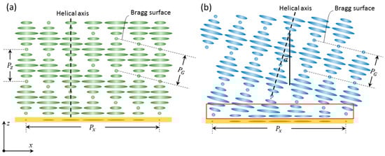
Figure 6.
The PVGs LC director configurations consisted of (a) planar-PVGs, where the helical axis was oriented perpendicular to the substrate surface, the arrows labeled Pz and Px indicate the periodicity along the z and x axes, respectively. The dashed line represents the helical axis, and PG denotes the Bragg surface. and (b) slanted-PVGs, where the helical axis was parallel to the Bragg surface. The red box symbolizes the intermediary area between a level and inclined structure the arrows again show the periodicity along Px and the helical axis with angle α, with the PG indicated. The red box highlights the significant region of periodicity., which improves from ref. [112] with permission from the crystals.
In this scenario, Pz is equivalent to the pitch of the CLC, which is denoted as PCLC. Pz represents the periodic modulation of the grating along the z-axis, which is typically aligned with the propagation direction of light through the grating. This modulation determines how light interacts with the PVG and contributes to its anisotropic behavior, where distinct periodicities along the transverse Px and longitudinal Pz axes influence diffraction properties. Pz also plays a crucial role in defining the overall grating period (PG) and impacts on the diffraction efficiency, with smaller Pz values enhancing light-grating interactions and improving performance for specific wavelengths or polarization states. Additionally, the interaction of Pz with incident light determines the angular and spectral characteristics of the diffracted light, making it essential for optimizing PVG performance in systems like AR displays and optical filters. The observed planar structure corresponds to our conceptual comprehension, as all LC directors adhere precisely to the bottom planar alignment. In addition, the Pancharatnam-Berry phase, which is a geometric phase, has been observed in transmissive LC polarization gratings and CLC structures. The rotation of the helical axis generates a geometric phase that can be utilized to create diverse optical components. Thus far, the planar structure has provided a plausible explanation for several experimental data points.
Equation (3) shows that the bulk free energy density of the planar structure is nonzero and varies inversely with the square of (Px). If Px is significantly larger than the pitch of the CLC, any deviation from completely relaxed circumstances will not be perceptible. However, Px eventually decreased to a level like the length of the CLC pitch as the deflection angle of the PVGs increased. The bulk free energy was so high that the system became unstable. The formation of planar-PVGs requires a large Px (where planar-PVGs and slanted-PVGs are indistinguishable) or strong anchoring and small thickness (less than 300 nm for each layer, and repeated spin-coating to achieve a sufficient thickness of approximately 3 m). The reflection efficiency, wavelength response, and angular response of planar PVGs and slanted PVGs are similar, except for their polarization selectivity. Therefore, in terms of practical implementation, it is more advantageous to use slanted PVGs constructed using a single assembly process. Unless otherwise specified, the PVGs we are referring to are the diagonal ones [113].
4. Fabrication Methods for PVGs
4.1. The Basic Preparation Process and Materials
4.1.1. Active and Passive PVGs
PVGs structures are mainly formed through the self-organization of CLC molecules, guided by surface alignment patterns. Presently, there are two main methods for creating PVGs devices. The first method, illustrated in Figure 7a, involves producing a film-like passive PVGs by initially applying a photo-alignment (PA) layer to a substrate. This layer is then subjected to patterned polarized light exposure, followed by the application of CLC reactive mesogens (RM). The film is subsequently fully cured with ultraviolet (UV) light. The resulting PVGs acts as a stable film, with its stability largely reliant on the crosslink density of the selected CLC-RM material system after curing [5,72,108]. Additionally, PVGs can function as active devices [114]. The process for creating active PVGs is akin to that used for conventional LC devices. It involves using an LC cell technique to introduce partially polymerizable CLC materials into a properly aligned cell, which includes two transparent electrode plates, as shown in Figure 7b. Consequently, active PVGs may display varied reactions to different stimuli based on their individual material composition, including voltage, frequency, and light.
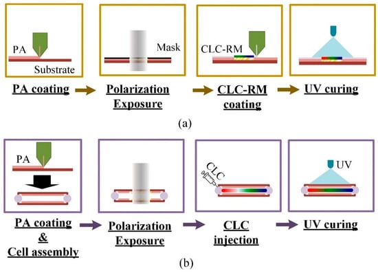
Figure 7.
Two PVGs preparation processes: (a) passive PVGs and (b) active PVGs.
4.1.2. Gradient-Pitch PVGs
Gradient-pitch PVG structures refer to LC-based devices where the pitch (the distance between adjacent helical structures) varies continuously or in discrete steps across the device. In these structures, the pitch gradient allows for tunable optical properties, such as selective wavelength reflection or transmission. By modulating the pitch along the structure, the grating can be tailored to reflect different wavelengths of light at different positions, enabling dynamic control over optical behavior. This gradient in pitch can be achieved through various means, including applying external fields (electric or magnetic) to adjust the orientation of LC molecules or through photopatterning techniques. These gradient-pitch PVGs are particularly useful in applications like tunable optical filters, beam steering, and displays, where precise control over light interaction is needed [115].
Figure 8a illustrates the schematic of a single unit with 16 gradient regions in a PVG sample, fabricated using a customized gradient photomask. The photomask, with 35,500 repeated units, features a 4 × 4 region with gradually varying transmittance (37% to 7%) designed based on UV exposure dosage, leading to two types of gradient pitch in CLC arrangements along the xz and y axes. Figure 8b illustrates a single unit with 16 gradient regions (R1–R16) in the x-z plane of the PVG sample, where CLCs twist vertically along a slanted helix axis. The pitch gradually decreases from R1 to R16 due to reduced UV exposure and dye absorption, with the longest pitch at the top and shortest at the bottom. Figure 8c illustrates the orientation of SD-1 molecules, with the horizontal period at the bottom surface in the x-z plane, used to precisely align the LC molecules in the horizontal plane. The angle φ represents the tilt of the grating vector K [116].
The schematic fabrication process of reflective PVGs with gradient periods, as described in Figure 8d. The glass substrate was cleaned sequentially with acetone, isopropyl alcohol, and ethanol. A 1 wt.% solution of the photo-alignment material azobenzene sulfonic dye (SD-1) in dimethylformamide was spin-coated onto the cleaned substrate at 500 rpm for 5 s, followed by 3000 rpm for 30 s to form a uniform thin film (step i). The film was then dried on a hotplate at 100 °C for 10 min. To create the photo-alignment pattern, the SD-1-coated substrate was exposed to left-handed and right-handed circularly polarized light from a two-beam interferometer, generating a PB grating pattern (step ii). The PVG precursor, a mixture of RM257, chiral dopant R5011, photo-initiator Irgacure 651, UV dye (Avobenzone, Shanghai, China), and surfactant (Zonyl 8857A), was then spin-coated onto the exposed substrate. The mixture was first applied at 500 rpm for 30 s, then heated on a hot stage at 80 °C for two minutes to remove the toluene solvent and promote self-alignment of the chiral liquid crystal (step iii). Finally, the PVG sample was cured under UV light at 60 °C using a photomask with gradient transmittance (step iv) [117].
Figure 8e illustrates the optical setup for two-beam interference. A linearly polarized Ar+ laser beam (λ = 488 nm) was expanded and collimated using a lens, then split into two beams (s and p waves) by a polarizing beam splitter (PBS) cube. A half-wave plate (HWP) was placed before the PBS to ensure equal intensity for both beams. The beams then passed through a quarter-wave plate (QWP) to convert them into opposite-handed circularly polarized beams. The glass substrate coated with SD-1 was positioned in the interference path to receive the PB grating pattern. In this setup, the UV light exposure dosage was 5 J/cm2, the angle between the two beams was 2θ = 59°, and the estimated horizontal period of the grating pattern was λ = 495 nm.

Figure 8.
(a) Schematic representation of a single unit featuring 16 gradient regions in the PVG sample and arrows R1, R4, R13, R16 indicate light wave vector directions in a periodic structure, with the x, y, and z axes labeled. (b) Schematic profile illustrating four distinct regions in the PVGs along with the orientation of SD-1 molecules at the bottom and arrows show the diffraction patterns along the x, y, and z axes, with the angle α representing the grating’s angular orientation. (c) Schematic cross-sectional view of LC molecules within one period length arrows K, Δx, and Δy indicate the wave vector direction and the periodicity along the x and y axes. (d) Diagram illustrating the fabrication process of reflective PVGs with gradient periods and arrows show light exposure (LCP, RCP) during the fabrication process, including spin-coating, UV exposure, and curing. (e) Schematic of the optical configuration for two-beam interference and arrows depict the optical path of laser light through various components, including a half-wave plate (HWP), polarizing beam splitter (PBS), mirrors (M1, M2), and quarter-wave plates (QWP1, QWP2) towards the sample. Reprinted with permission from [118] © Optical Society of America.
4.1.3. Liquid Crystal Materials
The CLC materials for passive PVG typically comprise a combination of nematic RM, chiral intermediates, and photo-initiators, all dissolved in volatile solvents. Figure 9a illustrates the chemical structures of some materials frequently utilized in the primary components of PVGs. Diacrylate-type reactive RM monomers, characterized by acrylate functional groups at both ends, serve as the main constituents for the synthesis of solid-state RM networks, as shown in Figure 9b [119]. The integration of RM materials with varying spacer lengths, particularly those with flexible carbon chain lengths, is a conventional approach in the optimization of LC materials. This blending facilitates the formation of mixed crystals with appropriate phase transition temperatures or viscosities, aiming to enhance performance and optimize the preparation process. Comprehensive research has been undertaken on these materials, including an examination of RM materials relevant to film manufacturing methodologies available in references [120,121]. Studies demonstrate that the film-forming properties and grating architecture of PVGs can be improved by optimizing monomer composition, engineering solvents, and including additives.
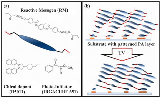
Figure 9.
(a) Examples of key components in liquid crystal materials for passive photonic devices include RM, chiral dopants, and photo-initiators. (b) Schematic representation of the polymerization process of cholesteric phase RM materials in PVGs following UV light exposure [122].
Conversely, active PVGs provide a wider array of LC material options, facilitating the selection of an appropriate formulation tailored to specific application needs. Chen et al. [123] It was proved that the response of PVG devices to electric field frequencies and light may be attained utilizing dual-frequency liquid crystals infused with azobenzene chiral dopants. Li et al. [114] effectively managed the efficiency of PVGs through voltage control. These examples demonstrate the capability of active PVGs to provide controllable and tunable optical responses, positioning them as a significant area of research for advanced optical and electronic devices. Passive PVGs exhibit excellent compatibility with existing waveguide coupling methodologies for diffractive optical waveguide (DOW-AR) applications, owing to their thin film deposition technique and environmental resilience. This feature simplifies the process of creating PVGs on waveguide substrates as coupling gratings, making it a favored option in this field of study. Active PVGs enhance the ability to manipulate and adapt to achieve specific optical responses when exposed to external stimuli. These qualities can lead to innovative designs and uses for AR devices, positioning them as a valid research focus.
4.2. Polarization Exposure
A periodic alignment pattern can be produced through the superposition interference of two coherent beams: one with left circular polarization (LCP) and the other with right circular polarization (RCP), as shown in Figure 10a. By integrating polarizing optical components, such as wave plates, into a standard holographic exposure system, a polarized interference exposure setup for PVGs can be achieved, as depicted in Figure 10b. When these two beams, each with a wavelength of λ, are symmetrically aligned relative to the vertical axis of the substrate and meet at an angle of 2θ, the resulting spatial period dx can be calculated as:
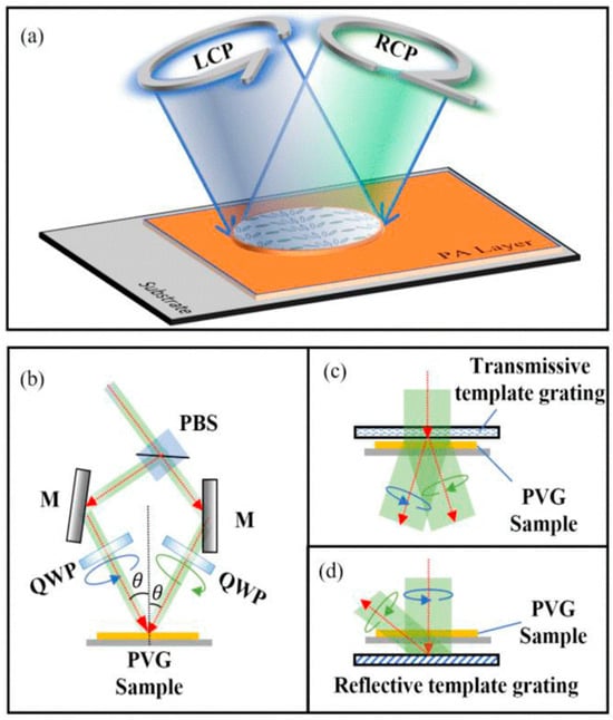
Figure 10.
(a) Setup for photo-alignment exposure in PVGs fabrication and the arrows indicate LCP and RCP light being incident on the photoalignment (PA) layer on the substrate. The light interacts with the PA layer, affecting its orientation. (b) Polarization interference diagram illustrating two beams of circularly polarized light exhibiting orthogonal rotational characteristics. Polarized holographic configuration. The arrows represent light passing through a polarizing beam splitter (PBS) and being reflected by mirrors (M) after passing through quarter-wave plates (QWP), with the angle θ showing the rotation of the polarization as it interacts with the sample on the PVG. Holographic imprinting utilizing (c) transmissive and the arrows show light interacting with a transmissive template grating. The incident light is diffracted by the template grating and interacts with the PVG sample at specific angles. (d) reflective template gratings the arrows represent light interacting with a reflective template grating, with the diffraction and reflection patterns shown as the light interacts with the PVG sample at different angles [122].
It is crucial to recognize that, akin to other interferometric exposure techniques, the two exposure beams used in the PVGs surface alignment process might exhibit asymmetry. It is vital to ensure that the light intensity hitting the substrate remains uniform, ideally maintaining a 1:1 ratio. This consistency is key to forming stable linearly polarized electric field oscillations within the PA layer, enabling the PA material molecules to gather energy in a specific polarization direction, thereby enhancing PA quality.
When choosing an asymmetric exposure, it is crucial to individually calculate and adjust the projected light intensity and the polarization state ellipticity on the substrate plane for each exposure beam. The interference of reflected beams at different angles of incidence on the substrate must be taken into account. Higher exposure angles result in shorter interference periods, particularly in symmetric structures that can accommodate a broader range of exposure angles. This flexibility in exposure angles allows for the creation of lower period interference cycles. Consequently, due to the straightforwardness and reliability of the preparation process, symmetric exposure is typically advised. The holographic exposure technique enables quick, high-resolution alignment patterning over large areas. However, a laser source with a long coherence length and a vibration-stable exposure stage is generally required to ensure high-quality interference.
Besides the traditional holographic exposure system utilizing a beam splitter or polarized beam splitter (BS/PBS) to create two coherent polarized lights, an alternative method called “holographic imprinting” can be utilized. This way requires the template grating to create two orthogonal beams of circularly polarized light through diffraction, thereby establishing an interference field in the overlapping region [124].
In 2009, Nersisyan et al. [125] utilized a Pacharatnam-Berry (PB) transmission grating as a model to produce two orthogonal circularly polarized beams (+1st and −1st orders) for interference, as depicted in Figure 10c. This approach enabled them to fabricate a PB grating with a 2.5 μm period. However, achieving a smaller period is challenging due to the limited diffraction angle of PB gratings, which typically does not exceed 15°. Recently, researchers have proposed alternative methods to overcome this limitation by using PVGs as template gratings. In 2023, Fang et al. [126] and Ye et al. [127] independently introduced a technique that employs two stacked transmissive PVGs as templates to generate two diffractive beams with a significant angular separation for interference. This method has demonstrated the capability to achieve a reduced period with submicron precision effectively.
Reflective PVGs can function as template gratings for holographic imprinting, as demonstrated in Figure 10d. In 2022, Xiong et al. [128] introduced a method utilizing the interference between the +1st and 0th orders of a reflecting photonic crystal to create a PA pattern with a period of 0.6 μm. This method streamlines the procedure by employing the incident light from the template grating for interferometric exposure, thereby eliminating interference from other diffraction orders in the interference field. This strategy can yield superior interference patterns.
The protocols for PVG exposure outline that the two coherent beams responsible for creating interference can originate from either the same side of the substrate (Figure 10b,c) or from opposite sides (Figure 10d). In traditional volume grating production, this difference usually involves altering the spatial orientation of the grating vector, leading to the development of either a transmissive or reflective volume grating [129]. However, in the case of PVGs, the interference exposure mainly results in periodic patterns within the PA layer on the substrate’s surface. The PA layer’s typical thickness, being just a few nanometers, is insufficient to create volume effects. The creation of a transmissive or reflective photonic volume grating (PVG) is largely influenced by the periodicity perpendicular to the substrate’s orientation, as determined by the cholesteric phase in the subsequent liquid crystal layer [106]. The transmissive or reflective nature of PVGs is not affected by the orientation of the interfering beams, whether they strike the same side or opposite sides of the substrate. Nonetheless, during the exposure process, several potential issues must be considered that could affect the quality of the diffraction patterns. For transmissive templates, it is crucial to minimize the impact of the zeroth-order transmitted light on the interference pattern. For reflective templates, interlayer interference between substrate surfaces must be carefully managed. These challenges can be addressed by improving the template grating design, adjusting the intensity and polarization of the incident light, and using suitable substrate coatings or refractive index matching materials [130,131,132].
5. Optical Properties
To comprehensively showcase the diffraction properties of PVGs, a meticulous simulation model was developed using a commercially accessible Finite Element Method (FEM) program. When analyzing PVGs, it is crucial to evaluate several key attributes, including diffraction efficiency, wavelength response, angular response, and polarization response [133,134,135,136]. Based on the findings shown in Figure 11a, only light that is circularly polarized and has the same handedness as helical rotation undergoes diffraction. In this case, the RCP is diffraction-prone, whereas the LCP is unaffected. Moreover, in the case of Bragg volume gratings, PVGs must possess sufficient thickness to effectively induce Bragg diffraction. Figure 11b illustrates a clear correlation between the diffraction efficiencies [82].
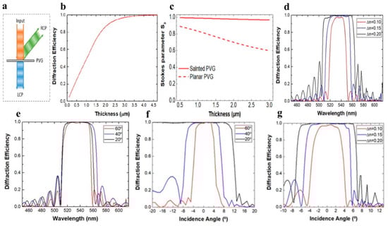
Figure 11.
(a) Diagram of a PVGs-diffracted beam; (b) Diffraction efficiency simulated as a function of layer thickness; (c) Stokes parameters S3 against film thickness; (d) diffraction efficiency spectra at 50° diffraction angle and normal incidence with varying refractive index contrast; (e) various diffraction angles with Dn = 0.15. (f) Three refractive indices contrast with 50° diffraction angles; (g) three diffraction angles with Dn = 0.15. The diffraction efficiency with respect to the incident angle improved from Ref. [112] with permission from the crystals.
The diffraction efficiency initially exhibited a monotonically increasing trend as the thickness increased, followed by a gradual saturation and convergence of 100%. Hence, the optimal thickness to achieve high diffraction effectiveness for a specific wavelength can be readily derived by considering the number of pitches. The thickness of a PVGs is significantly smaller, measuring only a few micrometers, in contrast to a standard VHG, which typically has a thickness of tens of micrometers. Additionally, it is crucial to acknowledge that the efficiency discussed pertains only to circularly polarized input. It should be noted that PVGs allows for complete transmission of the opposite circular polarization. This characteristic offers a significant level of light transmittance to the surrounding environment, which holds considerable significance for transparent near-eye displays [135,136,137,138,139,140].
As shown in Figure 11c, the analysis of polarization properties is an essential aspect that has received limited attention in previous studies. However, it is imperative to investigate these features to effectively utilize PVGs in cascaded optical systems, where precise polarization control is crucial [141]. According to the preliminary analysis, when the input circular polarization is appropriate, the first-order diffracted light maintains circular polarization. In the context of this discussion, it was observed that when circularly polarized light is incident upon reflective or transmissive PVGs, it maintains its original handedness or undergoes a reversal in handedness. Subsequently, Xiang et al. discovered transmissive PVGs and observed a significant deviation from circular polarization in the first-order polarization state, as reported in their study. This finding was further verified through modeling. In a recent study, Lee et al. analyzed the polarization response of PVGs [113,142].
A quantitative metric used to examine the polarization characteristics of the diffracted light is the Stokes parameter S3. The magnitude of the circular polarization that light exhibits is indicated by sign S3. For instance, when S3 = 1, RCP light is present. In contrast, an S3 equal to −1 indicates the presence of LCP light. The simulation demonstrated that the horizontal period (Px) was 440 nm and the vertical period (Pz) was 205 nm. Consequently, this gives rise to an inclined orientation of the central wavelength, pre-established as 532 nm, whereas the measured value of Dn is 0.15. In the context of diagonal design, when the angle of incidence is perpendicular, the first-order polarization condition strongly resembles circular polarization, as illustrated in Figure 5d. On the other hand, the light emanating from the PVGs exhibits a significant departure from circular polarization due to diffraction.
A previous study on the response of polarization led to the discovery of a tilted arrangement of the PVGs. Nevertheless, it is important to acknowledge that the analysis of the polarization response is the initial phase. Both the inclination angle and the angle of incidence significantly affected the polarization response. A more comprehensive examination is required to thoroughly comprehend the optical reaction of subject matter. PVGs Bragg diffraction is known to be dependent on the helical twist that occurs along the optical axis of the LC. As a result, the fundamental factor influencing index modulation in PVGs is the birefringence of LC material. As a result of improvements in the LCD industry, a wide range of birefringence values is available, ranging from n = 0.05–0.4. The reflecting band of PVGs, such as the spectral features of CLC, can be easily modified using an LC with various refractive index variations (n), as shown in Figure 11d. Typically, as the refractive index (n) increases, the width of the reflection band also increases. Figure 11e displays the diffraction efficiency spectra at three distinct diffraction angles with a refractive index of 0.15. Based on the obtained simulation findings, it is evident that the diffraction efficiency and bandwidth exhibit negligible correlation with the diffraction angle. This characteristic of PVGs allows for efficient diffraction of light at various angles, making them highly advantageous for near-eye display systems.
The investigation and illustration of the angular response across various levels of birefringence are shown in Figure 11f. As the difference in the refractive index (Dn) increases, so does the angular width of the incident light band. In contrast to VHG’s modest effective index modulation, often on the order of 10−2, LC’s birefringence of the LC is substantially higher, typically approximately 0.15. As a result, PVGs have a more comprehensive range of angular bandwidths, which is vital in various applications, including the use of light couplers in near-eye systems. The previously listed topics are discussed later. It is worth noting that the diffraction angle influences the angular response. Figure 11g shows the angular bandwidth for various diffraction angles while maintaining a constant Dn value of 0.15. The observed pattern indicates that as the angle of diffraction increases, the range of incident light angles that results in high diffraction efficiency becomes wider [112].
6. Applications of Polarization Volume Gratings in DOW
PVGs are optical elements with unique diffraction characteristics and the capability for large-scale production due to efficient and economical manufacturing processes, making them an attractive option for various optical uses. PVGs have demonstrated significant promise and progress as DOW coupling components in AR display technologies. This section seeks to examine the latest research progress concerning the application of PVGs in DOW-AR systems.
6.1. EPE Function and Diffractive Optical Waveguide Working Principles
Diffractive optical waveguides (DOWs) are optical instruments that utilize diffractive components, like gratings, to couple and guide imaging light through a slender, transparent waveguide [83]. Figure 12 demonstrates the fundamental principle of DOWs by depicting a waveguide system featuring at least two grating sections that function as in-couplers and out-couplers. When the collimated light field from the image projector enters the in-coupling grating, it experiences diffraction [142,143,144,145,146,147,148,149,150,151,152,153,154]. The angle of diffraction exceeds the waveguide medium’s total internal reflection angle, which confines the diffracted light within the waveguide, allowing it to travel along the structure. Upon interacting with the out-coupling grating, the propagating light is diffracted again, breaking the waveguide’s total internal reflection condition. This process allows the light to exit the waveguide and be visible to the human eye. To prevent dispersion due to grating momenta within the waveguide system, it is crucial that the sum of the grating vectors of all coupling gratings in the waveguide plane equals zero. This also ensures the angular consistency of both the incoming and outgoing light.
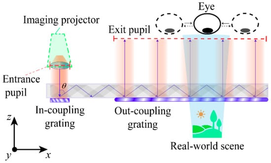
Figure 12.
Basic schematic illustration of the DOW system [122].
The EPE feature of DOWs is typically accomplished by adjusting the local diffraction efficiency within the out-coupling grating. This adjustment enables a portion of the light energy traveling through the waveguide to be diffracted at each diffraction point, while the rest of the light continues its journey within the waveguide. As the light moves along, it undergoes diffraction at multiple reflection points on the grating, resulting in repeated output and continued propagation. This mechanism enhances the light output in the out-coupling area and increases the size of the exit pupil, as shown in Figure 12. A larger exit pupil allows for a wider eye box, accommodating a greater range of eye movements for viewers and permitting a reduction in the size of the imaging projector aperture. Consequently, this reduces the overall volume and weight of the waveguide system, making DOWs a more favorable optical solution compared to other options.
The design depicted in Figure 12 enables one-dimensional electrostatic potential energy simply along the x-axis. The optical pupil size in the y-direction decreases with increasing propagation distance. To attain sufficient eye box size in both dimensions, a 1D-EPE waveguide typically requires an extended entrance pupil. This indicates that the size of the entrance pupil in the non-expanded direction (y-direction) must be considerably greater than in the expanded direction. Thus, additional diminishment of the image projector’s dimensions and mass for the 1D-EPE waveguide configuration poses difficulties [155,156,157,158,159,160,161,162,163,164].
To ensure pupil expansion across the entire waveguide plane, a DOW should be configured as a two-dimensional 2D-EPE structure. Figure 13a depicts a traditional “L-shaped” 2D-EPE setup [165], which includes an additional steering grating within the waveguide system. This steering grating directs light from the in-coupling grating within the waveguide plane, allowing for the reproduction and dispersion of light in multiple directions from the out-coupling grating. The presence of the steering grating means that the grating vectors of the in-coupling and out-coupling gratings cannot be parallel within the waveguide plane, facilitating the sequential duplication and propagation of light in two distinct directions. The basic “L-shaped” design comprises three coupling gratings, all of which can be one-dimensional (linear) gratings, leading to the sequential expansion of optical pupils in various directions. Alternatively, another type of 2D-EPE structure employs a two-dimensional (crossing) grating to combine the functions of steering and out-coupling gratings [166]. Figure 13b shows that the crossed grating consists of two primitive vectors, Go1 and Go2, which enable the steering of propagating light while simultaneously expanding the exit pupil in different directions. This structure offers several benefits over the “L-shaped” design, such as a smaller waveguide size, reduced diffractive interaction loss, and enhanced fabrication tolerance. These advantages contribute to high imaging quality while keeping fabrication costs low.
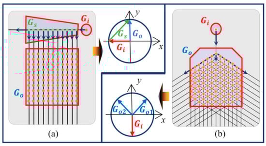
Figure 13.
Illustration of typical two-dimensional (2D-EPE) structures in DOW systems. (a) The “L-shaped” configuration and the arrow labeled Gi represents the incident wave vector, indicating the direction of the incoming wave. The Gs arrow represents the scattered wave vector, showing the direction of the diffracted wave after interaction with the grating. The Go arrow indicates the original wave vector direction, which is parallel to the grating’s surface. (b) the “crossed” grating configuration and the arrow labeled Gi indicates the incident wave vector in a new orientation, while the other arrows, Go and Gs, show the directions of the outgoing and scattered waves. The hexagonal pattern of the grating in this panel suggests a different geometry, and the arrows highlight the corresponding wave vectors in this configuration [7].
6.2. Advantages of PVGs Coupler for DOW Applications
For waveguide coupling to function effectively, the coupling grating must generate a diffraction angle large enough to keep the diffracted light confined within the waveguide under total internal reflection (TIR) conditions. The grating vector’s range within the waveguide plane must meet the following criteria:
In this scenario, ko denotes the wave vector of the incoming light, n defines the refractive index of the medium around the grating, θi represents the angle at which the light hits the medium, and m signifies the diffraction order. To avoid crosstalk, only the first-order diffracted light (m = ±1) is permitted to propagate. For illustration, we consider the grating vector Gx in the waveguide plane (xy-plane) to be oriented along the x-axis, and the refractive index of the medium surrounding the grating is consistent in both reflective and transmissive fields. Figure 14 shows the diffraction characteristics and k-vector diagram of an in-coupling grating.
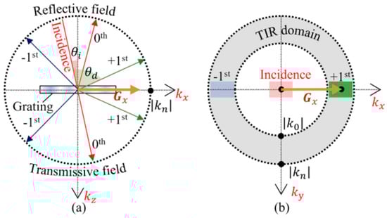
Figure 14.
(a) Diffraction behavior and the incidence arrow represent the incident wave vector, with an angle θd relative to the grating’s surface. The grating vector, Gx, is parallel to the grating’s periodic structure, indicating the direction of the grating’s spatial frequency. The arrows labeled +1st, 0th, and -1st indicate the diffraction orders of the reflected and transmitted fields, corresponding to different directions of diffracted light. The reflective field and transmissive field arrows represent the diffracted light components in the reflected and transmitted directions, respectively. (b) k-vector diagram of the in-coupling grating in a DOW system and the incidence arrow represents the direction of the incident wave vector in the x-y plane. The Gx arrow shows the projection of the grating vector along the x-axis. The TIR domain (Total Internal Reflection domain) is indicated by the shaded region, with the k0 vector showing the magnitude of the incident wave vector in the absence of diffraction. The diffraction orders +1st and -1st are represented, showing the direction of diffracted light in the x-y plane [7].
To attain superior imaging performance, DOW applications frequently necessitate in-coupling gratings that exhibit highly efficient single-order diffraction properties, concentrating the main diffraction energy at either the +1 or −1 order. The diffraction efficiency of out-coupling gratings is generally adjusted at different positions to enable pupil expansion. However, it requires a single-order diffraction capability, and the diffracted energy must be confined to the reflective or transmissive field to prevent the output light from exiting the waveguide in an unintended direction. The coupling grating period within the waveguide plane (2π/|Gx|) is usually at a subwavelength scale to satisfy Equation 5. At this scale, achieving these performance standards with traditional gratings is difficult. SRGs are commonly used as waveguide coupling gratings, with the grating surface’s morphology influencing their diffraction characteristics. The existing literature indicates that a standard SRG with a quasi-sinusoidal profile can attain a diffraction effectiveness of up to 34% [167]. Conversely, a binary (rectangular) relief profile can attain diffraction efficiencies of up to 41% [167]. Nevertheless, as the SRG period attains the subwavelength scale, an asymmetric shape is generally necessary to provide satisfactory diffraction efficiency.
Blazed gratings, a type of asymmetric SRGs have demonstrated diffraction efficiency above 55% for subwavelength periods [168]. In the case of more intricate topologies, such as the inclined grating structure documented in [169], the efficiency may exceed 80%. However, the fabrication of intricate morphological gratings at subwavelength periodic dimensions is very prone to manufacturing defects, potentially resulting in substantially increased production costs. As a result, SRG-coupling gratings have considerable processing difficulties and cost obstacles in mass production, despite the theoretical potential for attaining relatively high diffraction efficiency via intricate surface morphology [170].
The literature [171,172] indicates that typical optical efficiency ratings for SRG waveguide systems range from 50 to 200 nit/lm. However, when assessing power consumption and display brightness in outdoor environments, the challenges of optical efficiency remain the primary concerns for contemporary SRG-based DOW-AR systems. [122]. Conversely, PVGs provides a maximum diffraction effectiveness above 80% with a more straightforward and economical preparation method [173]. Consequently, PVGs possess the capability to improve the effectiveness of diffractive waveguides while decreasing the related preparation expenses. A PVG waveguide prototype created in [7] further substantiates this possibility, exhibiting a waveguide system efficiency of 441 nit/lm. Conversely, VHGs provide the benefit of attaining exceptionally high single-order diffraction efficiency, approaching 100%, through a relatively straightforward production procedure, rendering them a cost-effective option for the development of efficient waveguide coupling gratings. However, the wavelength and angular bandwidth of VHGs provide challenges in meeting the requirements for FOV and color representation in DOW-AR applications, due to the limitations imposed by the material’s refractive index contrast [174]. Initial VHG-based waveguide systems typically possess a FOV of less than 20° [102].
Recent research indicate that the response bandwidth of VHGs can be markedly enhanced through multiplexing design or by combining with additional optical components, such as free-form surfaces. Nonetheless, these methods typically need exact alignment and lamination processes, hence increasing production complexity and cost. Therefore, continuous research and development are crucial to improve the performance and reliability of VHG-based waveguide systems. Considering the existing limits of coupling grating technology and the diffractive features of PVGs, it can be concluded that PVGs presents numerous potential benefits as a waveguide coupling grating, including:
(a) Elevated single-order diffraction efficiency, ensuring optical efficacy within the waveguide and reducing backward light leakage. (b) Expandable bandwidth range that ensures adequate field of view and color accuracy. (c) Polarization selectivity enhances the transmission of external ambient light at the exit pupil region while reducing the “rainbow pattern” phenomenon caused by the diffraction of external ambient light (d). The efficient and cost-effective approach for mass production. These advantages establish PVGs as a feasible substitute for waveguide coupling elements and have prompted researchers to extensively investigate their potential in AR applications.
6.3. Recent Advances in PVGs-Based DOW-AR Applications
Beyond an extensive examination of the physical properties, preparation methods, and optimization techniques of PVGs, significant progress has been made in exploring their capability for waveguide coupling. This section explores and assesses the recent advancements in using PVGs for DOW-AR applications.
PVGs-based waveguide systems, as a variant of DOW technology, exhibit core concepts and reasoning akin to other grating-based waveguide technologies. Consequently, numerous design and research outcomes pertaining to the performance of DOW systems can be utilized in the design and optimization of PVGs waveguides, albeit originally for a distinct sort of linked grating technology. A plethora of studies and conclusions pertain exclusively to PVG-based waveguide applications, owing to the unique optical characteristics of PVG couplers. We highlight several of these investigations herein.
6.3.1. Full-Color Imaging and FOV Optimized
Diffraction waveguide technology enables color displays by permitting the concurrent transmission of light fields in red (R), green (G), and blue (B) wavelengths. The most straightforward method involves directing the red, green, and blue images through three distinct waveguides, theoretically ensuring that the RGB channels remain entirely separate. This separation allows for the individual optimization of each channel, which can enhance both the field of view and color performance. This method has limitations related to waveguide thickness and production costs, stemming from the necessity to individually prepare and integrate three layers of waveguides. In 2018, researchers introduced a dual-layer PVG waveguide structure to deliver a comprehensive color AR display [108]. Figure 15 illustrates that the wavelength multiplexing design of PVGs-couplers enables the propagation of two channels, green and blue, within a single waveguide medium. Conversely, the alternative waveguide is designated solely for the propagation of red light.
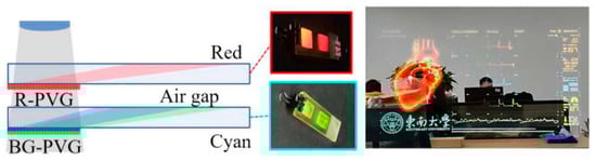
Figure 15.
Double-layer PVG waveguide design to realize full-color AR display [108], reproduced with permission from The Optical Society.
This design enables the creation of a full-color AR display using PVGs waveguide technology, featuring a 35° diagonal field of view. However, the challenge arises when a single waveguide layer is used to carry two different wavelength ranges at once, as this complicates the process of achieving a wider field of view within the limited total internal reflection angle range of the waveguide substrate, due to the effects of grating dispersion.
To enhance the FOV, Gu et al. [81] examined the FOV efficacy in full-color PVG systems using various multilayer configurations and introduced an optimized two-layer PVGs waveguide design in 2022. This method partitions the picture light’s FOV in green into two segments, facilitating propagation through two separate waveguides. As a result, this method increases the FOV of a full-color PVGs waveguide to 45°, as demonstrated in Figure 16. Ding et al. [174] performed an extensive analysis of the FOV limit for single-layer PVGs color waveguides, emphasizing optimal gratings and waveguide properties, and provided a meticulous design optimization for color imaging in PVGs.
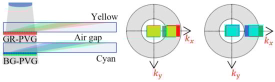
Figure 16.
Schematic diagram of the optimized two-layer PVGs waveguide scheme and the corresponding k-vector coupling principle. The arrows indicate the direction of light as it passes through the GR-PVG and BG-PVG layers. The different colors represent the varying wavelengths of light: red for the GR-PVG layer, blue for the BG-PVG layer, and yellow and cyan for the light passing through the air gap. The light diffracts according to the periodicity of the grating structure. The arrows labeled kx and ky represent the components of the wave vector in the x and y directions, respectively, in the diffraction pattern. The kx and ky directions correspond to the horizontal and vertical components of the diffraction wave vectors, showing how the light is diffracted by the grating at specific angles. The colored boxes in the diffraction diagram represent the diffraction orders of the incident light: red, yellow, cyan, and green correspond to different diffraction orders based on the grating structure, while the arrows indicate their respective directions in the kx and ky axes [128], reproduced with permission under the creative common’s attribution 4.0 license.
Yan et al. [122] recently developed a technique for creating three-dimensional gradient periodic PVGs. As shown in Figure 17, their approach involved crafting mask plates with two-dimensional variations in UV transmittance and enhancing LC materials by incorporating UV absorbers. The team successfully produced the required waveguides and confirmed the validity of their proposed method. The resulting gradient photonic volume gratings demonstrated an angular bandwidth of 61° and maintained a diffraction efficiency of 80%, with peak efficiency nearing 100%. The broader angular bandwidth facilitates an increased FOV for the PVGs waveguide, while the targeted adjustment of grating diffraction efficiency within the waveguide plane effectively enhances pupil exit uniformity.
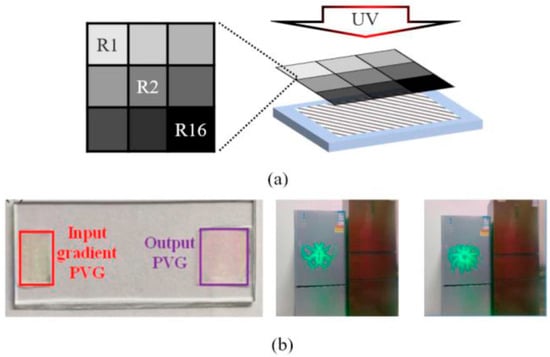
Figure 17.
PVGs featuring a three-dimensional gradient periodic structure achieved through regionalized UV curing intensity control [122]. (a) Schematic diagram of a mask plate featuring various UV transmittance cells and the UV curing process of PVGs. (b) The prepared waveguide sample and the imaging effect, reproduced with permission from The Optical Society.
In addition, compared to other coupling grating technologies, the polarization characteristics of PVG add another dimension for improving waveguide imaging. Recently, Chen et al. [175] presented a waveguide design with three channels that utilizes the polarization response of PVGs to distinguish imaging beams with different FOV ranges and transmit them separately. Numerical analysis indicates that this approach can achieve a substantial diagonal field of view of 90° for a PVGs waveguide.
6.3.2. Uniformity Enhancement Method of the Exit Pupil
The consistency of the exit pupil is an essential performance indicator for a DOW device. To achieve a uniform output intensity at different grating positions, the diffraction efficiency of the out-coupling grating can be adjusted locally [75,176]. In PVG couplers, this efficiency can be altered spatially by changing the thickness of the couplers. However, this approach complicates the preparation process and might affect the transmittance of ambient light. In 2018, Lee et al. introduced an innovative way for attaining uniform waveguide output by using the polarization selectivity of photonic crystal waveguides. Regulating the polarization state of propagating light facilitates the attainment of a consistent output for the PVGs waveguide. A layer of liquid crystal film with a certain thickness was incorporated in the out-coupling region, as illustrated in Figure 18a. The film can modify the polarization state of the incident light by propagating it at different locations on the out-coupling PVGs. This method enables the preservation of consistent thickness in out-coupling photonic crystal waveguides, hence allowing for localized efficiency regulation by the manipulation of the orientation of liquid crystal molecules in the supplementary layer.
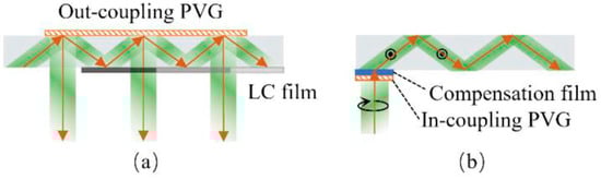
Figure 18.
Improving exit pupil uniformity in PVGs waveguides involves (a) adding an additional LC film in the out-coupling zone and the out-coupling PVG directs the diffracted light through the LC film. The arrows indicate the direction of light propagation as it is diffracted by the out-coupling grating, with different diffraction orders represented by the arrows pointing in various directions. These arrows demonstrate the path the light takes through the system after passing through the out-coupling PVG. (b) a compensating film in the in-coupling region and the arrows show the light interacting with both the in-coupling PVG and the compensation film. The incident light is directed through the system, and the arrows indicate the light’s path after passing through the in-coupling PVG. The dashed arrows show the direction of the light as it enters the compensation film, with the circular arrow indicating the rotation or adjustment of the light within the system. This configuration adjusts the diffraction and light propagation through the layers [122].
Ascertaining the polarization state of propagating light within the waveguide is arduous due to its fluctuation with each total internal reflection bounce. Light traveling at varying angles experiences unique polarization alteration trajectories, resulting in different polarization states at many sites. This variability complicates the design of polarization modulations in the out-coupling area. Feng et al. [177] presented a resolution to this problem by introducing a compensating film to sustain a consistent polarization state of light during propagation. As illustrated in Figure 18b, a compensation film can be added following the transmissive in-coupling PVGs to alter the polarization state of the diffracted light from circular to linear (either s-polarization or p-polarization). This adjustment ensures that each TIR maintains the polarization of the light as it propagates, thereby aiding in the subsequent enhancement of exit pupil uniformity [117,118].
6.3.3. Two-Dimensional Pupil Expansion
Cui et al. [110,177] implemented the “L-shaped” scheme, typically utilized in contemporary DOW systems, to improve the effectiveness and functionality of PVGs waveguide solutions in 2021. This method facilitated the implementation of the 2D-EPE function for PVGs waveguides. In 2022, a novel 2D-EPE scheme for PVGs waveguide technology was introduced in [7], with the corresponding results illustrated in Figure 19. This scheme utilizes the principle of polarization multiplexing by designing the out-coupling PVGs as a composite grating, which concurrently achieves deflection of propagating light in multiple directions and facilitates unidirectional coupling output. This scheme necessitates only two grating regions, in contrast to the “L-shaped” structure, enabling a more compact grating layout and facilitating shorter light propagation distances. This approach minimizes light energy loss and scatters during waveguide propagation, facilitating subsequent device layout design.
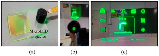
Figure 19.
The proposed 2D-EPE technique for the PVGs waveguide via multiplexing design was reprinted with permission from The Optical Society [7]. (a) Here are some pictures of how the prepared samples looked and the results of the AR imaging at were taken at distances of (b) 100 mm and (c) 18 mm from the waveguide.
In summary, these advances demonstrate the versatility and effectiveness of PVGs technology in addressing the challenges encountered in DOW-AR applications. Sustained research and development will likely reveal the potential of PVGs for various applications, providing promising optical solutions for AR devices.
7. Comparison and Prospects
Compared to macro-optics, combiners utilizing micro optics possess the advantages of smaller dimensions and reduced weight owing to the diffraction effect, which leads to a greater beam deflection angle. Consequently, these micro-optics-based combiners are highly amenable to miniaturization. In specific scenarios, it is possible to achieve an FOV exceeding 40°. The bandwidth allocated for the SRGs and PVGs is moderate, whereas the VHG has a relatively limited bandwidth. Nevertheless, existing diffraction waveguide combiners that rely on micro optics face several challenges. These include low efficiency levels below 10%, chromatic aberration issues in full-color displays, nonuniformity in illuminance, and a lack of mass-production processing technology. These obstacles have impeded the widespread adoption of these combiners in commercial applications. In addition, the presence of a significant angle and wavelength selectivity, as well as the occurrence of higher-order diffracted light in the diffractive waveguide, give rise to notable challenges in terms of dispersion and stray light, which can negatively impact the user’s overall experience. The limitations of SRG persist in the form of high cost and low efficiency. The laser exposure method can be utilized to obtain submicron machining precision in the fabrication of VHGs and PVGs [98].
The manufacturing procedure of holographic materials directly influences the evenness of the coating. In addition, the level of exposure is affected by the environmental stability requirements, which include parameters such as humidity, temperature, and airflow dynamics. Applying this specific exposure technique poses difficulties in achieving a mass-manufacturing procedure that maintains elevated levels of quality. Consequently, this hinders the extensive adoption and progress of applications designed for mobile devices. The implementation of roll-to-roll manufacturing technology has significantly streamlined the large-scale fabrication of waveguides. Nevertheless, achieving impeccable color waveguide processing without chromatic aberration remains a considerable obstacle, mainly because of the constraints imposed by the Bragg condition. The future enhancement of optical phenomena in existing combiners will depend on advancements in combining various solutions, manufacturing methodologies, and employing developing materials and display technologies. The design process encompasses several difficulties and possibilities, necessitating the incorporation of multiple solutions to create complex procedures and systems. The advancement of optical effects in micro- and nano-optics manufacturing remains reliant on substructure processing. Table 1 shows the comparison of different types of micro-optics.

Table 1.
Comparison of different types of micro-optics [178,179,180].
Incorporating complex-shaped substructures, which provide more design freedom, facilitate the achievement of broader bandwidths, and a high degree of precision in meeting design requirements, will affect the optical effects. Utilizing and incorporating components such as polymer nanoparticles will also achieve superior optical results, encompassing a decrease in optical chromatic aberration and higher imaging fidelity. The efficacy of VHG combiners also depends on the properties of the exposure and substrate materials. The phenomenon of exposure to VHG has exhibited notable advancements throughout its history, progressing from the utilization of silver halide and dichromate substances to the evolution of photo-induced polymer materials. Numerous academic investigations have recorded and analyzed the advancement in question [169]. The VHG waveguide system has improved its lightweight and shape, transitioning from classic glass substrates to contemporary resin substrates. Further research can be conducted on new micro-displays to develop specialized image sources, such as displays with specific polarizations and curved screens [181,182,183].
8. Conclusions
The paper concludes that AR-HMDs can be made thinner and lighter using grating devices based on micro-optical solutions. Planar diffractive waveguides employ subwavelength gratings to achieve light-coupling. The FOV and quality of the full-color display further influence the limitations in the development of diffractive waveguides. In the waveguide domain, it is vital to organize them into numerous layers to generate comprehensive color displays within the SRG waveguides. However, it should be noted that VHG waveguides sometimes require a complex three-step multilayer exposure procedure. This technique might lead to color crosstalk issues and present difficulties in achieving a full-color display with a large FOV. The integration of PVGs with LC results in a significant improvement in the diffraction efficiency and an increase in the FOV. This advancement aligns with ongoing research that focuses on developing AR-HMD combiners.
This study provides an overview of the current advancements in the physical concepts and manufacturing techniques employed in developing LC-based PVGs. It also investigates the different applications of these gratings in the development of novel optical technologies and forthcoming near-eye displays. The fabrication methods of PVGs, covering the key processes, essential materials, and related polarization exposure techniques used in their production. Following this, the review explores the applications of PVGs in DOWs, outlining the working principles of DOW systems. It highlights the advantages of using PVGs as couplers in DOW-AR applications, comparing them to other alternative schemes. Finally, the review discusses several recent advancements in PVG-based DOW-AR applications, such as full-color imaging, FoV optimization, exit pupil uniformity enhancement, 2D-EPE, and the integration of polarization volume lenses. This paper aims to provide valuable references and insights for future research and applications of PVG technology.
Advances in LC materials and optical systems have contributed to rapid progress in PVGs. PVGs have evolved from single-function gratings into multifunctional devices. Owing to their distinct and appealing optical features, PVGs have been efficiently used in creative optical systems to meet the expanding requirements of fundamental research and practical applications, including near-eye AR displays. Persistent and significant advancements, coupled with the introduction of innovative materials and hybridization methods, would facilitate the advancement of both PVGs and future-generation displays, thereby enhancing the quality of human existence.
Author Contributions
Conceptualization: A.Z. and S.S.; methodology: M.H.E.; writing—original draft preparation: A.Z. and S.S.; writing—review and editing: K.A. and M.H.E.; supervision: M.H.E.; project administration: M.H.E.; funding acquisition: M.H.E. All authors have read and agreed to the published version of the manuscript.
Funding
This research received no external funding.
Data Availability Statement
Not applicable.
Conflicts of Interest
The authors declare no conflicts of interest.
References
- Yin, K.; He, Z.; Xiong, J.; Zou, J.; Li, K.; Wu, S.T. Virtual reality and augmented reality displays: Advances and future perspectives. J. Phys. Photonics 2021, 3, 022010. [Google Scholar] [CrossRef]
- Kaur, R.; Pensia, L.; Kumar, R. Bragg degenerate model for fabrication of holographic waveguide-based near-eye displays. Appl. Opt. 2023, 62, 3467–3476. [Google Scholar] [CrossRef]
- Al-Ansi, A.M.; Jaboob, M.; Garad, A.; Al-Ansi, A. Analyzing augmented reality (AR) and virtual reality (VR) recent development in education. Soc. Sci. Humanit. Open 2023, 8, 100532. [Google Scholar] [CrossRef]
- Cevikbas, M.; Bulut, N.; Kaiser, G. Exploring the Benefits and Drawbacks of AR and VR Technologies for Learners of Mathematics: Recent Developments. Systems 2023, 11, 244. [Google Scholar] [CrossRef]
- Zia, A.; Saeed, S.; Man, T.; Liu, H.; Chen, C.X.; Wan, Y. Next-generation interfaces: Integrating liquid crystal technologies in augmented and virtual reality–A review. Liq. Cryst. Rev. 2024, 12, 30–56. [Google Scholar] [CrossRef]
- Wang, C.; Zhang, Y.; Weng, Y.; Shen, Z.; Wei, R.; Gu, Y.; Zhang, L. Holographic waveguide display with large field of view based on volume holographic grating. J. Soc. Inf. Disp. 2023, 31, 433–442. [Google Scholar] [CrossRef]
- Weng, Y.; Zhang, Y.; Wang, W.; Gu, Y.; Wang, C.; Wei, R.; Zhang, L.; Wang, B. High-efficiency and compact two-dimensional exit pupil expansion design for diffractive waveguide based on polarization volume grating. Opt. Express 2023, 31, 6601–6614. [Google Scholar] [CrossRef] [PubMed]
- Choi, M.; Han, H.; Min, W.; Min, K.; Han, D.; Shin, G. Recent applications of optical elements in augmented and virtual reality displays: A review. ACS Appl. Opt. Mater. 2024, 2, 1247–1268. [Google Scholar] [CrossRef]
- Tang, M.; Sun, C.; Ding, W.; Jiang, F.; Li, Y.; Li, W.; Lu, J. Full-color augmented reality display via integrated achromatic template polarization volume grating. Displays 2025, 103190. [Google Scholar] [CrossRef]
- Iadlovska, O.S.; Maxwell, G.R.; Babakhanova, G.; Georg, H.M.; Christopher, W.; Sergij, V.S.; Oleg, D.L. Tuning selective reffection of light by surface anchoring in cholesteric cells with oblique helicoidal structures. Opt. Lett. 2018, 43, 1850–1853. [Google Scholar] [CrossRef]
- Thapa, K.; Iadlovska, O.S.; Bisoyi, H.K.; Daniel, A.P.; John, M.D.S.; Corrie, T.I.; Quan, L.; Sergij, V.S.; Oleg, D.L. Combined electric and photocontrol of selective light reffection at an oblique helicoidal cholesteric liquid crystal doped with azoxybenzene derivative. Phys. Rev. E 2021, 104, 044702. [Google Scholar] [CrossRef] [PubMed]
- Simoni, F.; Francescangeli, O. Effects of light on molecular orientation of liquid crystals. J. Phys. Condens. Matter 1999, 11, R439–R487. [Google Scholar] [CrossRef]
- Lucchetti, L.; Kushnir, K.; Zaltron, A.; Simoni, F. Liquid crystal cells based on photovoltaic substrates. J. Eur. Opt. Soc. Publ. 2016, 11, 16007. [Google Scholar] [CrossRef]
- Nava, G.; Ciciulla, F.; Simoni, F.; Iadlovska, O.; Lavrentovich, O.D.; Lucchetti, L. Heliconical cholesteric liquid crystals as electrically tunable optical fflters in notch and bandpass conffgurations. Liq. Cryst. 2021, 48, 1534–1543. [Google Scholar] [CrossRef]
- Xiang, J.; Li, Y.; Li, Q.; Paterson, D.A.; Storey, J.M.D.; Imrie, C.T.; Lavrentovich, O.D. Liquid crystals: Electrically tunable selective reffection of light from ultraviolet to visible and infrared by Heliconical Cholesterics. Adv. Mater. 2015, 27, 3013. [Google Scholar] [CrossRef]
- Francescangeli, O.; Lucchetti, L.; Simoni, F.; Stanić, V.; Mazzulla, A. Lightinduced molecular adsorption and reorientation at polyvinylcinnamate-ffuorinated/liquid-crystal interface. Phys. Rev. E—Stat. Nonlinear Soft Matter Phys. 2005, 71, 011702. [Google Scholar] [CrossRef]
- Iadlovska, O.S.; Thapa, K.; Rajabi, M.; Mrukiewicz, M.; Shiyanovskii, S.V.; Lavrentovich, O.D. Electrically tunable total reffection of light by oblique helicoidal cholesteric. arXiv 2024, arXiv:2024:240408768. [Google Scholar]
- Jirón, V.; Rajabi, M.; Wang, H.; Lavrentovich, O.D. Dynamic control of active droplets using light-responsive chiral liquid crystal environment. Commun. Phys. 2024, 7, 200. [Google Scholar] [CrossRef]
- Nava, G.; Barboza, R.; Simoni, F.; Iadlovska, O.; Lavrentovich, O.D.; Lucchetti, L. Optical control of light polarization in heliconical cholesteric liquid crystals. Opt. Lett. 2022, 47, 2967–2970. [Google Scholar] [CrossRef]
- Lavrentovich, O.D. Design of nematic liquid crystals to control microscale dynamics. Liq. Cryst. Rev. 2020, 8, 59–129. [Google Scholar] [CrossRef]
- Li, B.-X.; Borshch, V.; Xiao, R.-L.; Paladugu, S.; Turiv, T.; Shiyanovskii, S.V.; Lavrentovich, O.D. Electrically driven three-dimensional solitary waves as director bullets in nematic liquid crystals. Nat. Commun. 2018, 9, 2912. [Google Scholar] [CrossRef]
- Xiang, J.; Varanytsia, A.; Minkowski, F.; Daniel, A.P.; John MD., S.; Corrie, T.I.; Lavrentovich O., D.; Peter, P.-M. Electrically tunable laser based on oblique heliconical cholesteric liquid crystal. Proc. Natl. Acad. Sci. USA 2016, 113, 12925–12928. [Google Scholar] [CrossRef]
- Liu, S.; Yu, H.; Jiang, M.; Ma, L.L.; Lu, Y.Q.; Wei, Q.H. Dual diffraction bands of heliconical liquid crystal gratings. Phys. Rev. Mater. 2024, 8, 085201. [Google Scholar] [CrossRef]
- Guo, Y.; Jiang, M.; Peng, C.; Sun, K.; Yaroshchuk, O.; Lavrentovich, O.; Wei., Q.H. Highâ resolution and highâ throughput plasmonic photopatterning of complex molecular orientationsin liquid crystals. Adv. Mater. 2016, 28, 2353–2358. [Google Scholar]
- Guo, Y.; Jiang, M.; Afghah, S.; Peng, C.; Selinger, R.; Lavrentovich, O.D.; Wei, Q.H. Photopatterned designer disclination networks in nematic liquid crystals. Adv. Opt. Mater. 2021, 9, 2170063. [Google Scholar] [CrossRef]
- Jiang, M.; Guo, Y.; Yu, H.; Turiv, T.; Lavrentovich, O.D.; Wei, Q.H. Low f-number diffractionlimited Pancharatnam–Berry microlenses enabled by Plasmonic Photopatterning of Liquid Crystal Polymers. Adv Mater. 2019, 31, 1808028. [Google Scholar] [CrossRef]
- Sato, S. Applications of liquid crystals to variablefocusing lenses. Opt Rev. 1999, 6, 471–485. [Google Scholar] [CrossRef]
- Ye, M.; Wang, B.; Sato, S. Liquid-crystal lens with a focal length that is variable in a wide range. Appl Opt. 2004, 43, 6407–6412. [Google Scholar] [CrossRef] [PubMed]
- Perera, K.; Haputhantrige, N.; Himel, M.S.H. M Mostafa, A Adaka, EK Mann, OD Lavrentovich Electrically tunable polymer stabilized chiral ferroelectric nematic liquid crystal microlenses. Adv Opt Mater. 2024, 12, 2302500. [Google Scholar] [CrossRef]
- Adaka, A.; Guragain, P.; Perera, K.; Nepal, P.; Almatani, B.; Sprunt, S.; Gleeson, J.; Twieg, R.J.; Jákli., A. A ferroelectric nematic liquid crystal vitriffed at room temperature. Liq. Cryst. 2024, 52, 1–9. [Google Scholar]
- Perera, K.; Haputhantrige, N.; Himel, M.S.H.; Mostafa, M.; Adaka, A.; Lavrentovich, O.D. AI Jákli Electrically tunable chiral liquid crystal lens arrays. Liq. Cryst. XXVII. 2023, 12658, 67–73. [Google Scholar]
- Alyami, A.; Rajapaksha, C.H.; Feng, C.; Paudel, P.R.; Paul, A.; Adaka, A.; Dharmarathna, R.; Lüssem, B.; Jákli, A. Ionic liquid crystal elastomers for actuators, sensors, and organic transistors. Liq. Cryst. 2023, 50, 1151–1161. [Google Scholar] [CrossRef]
- Karaszi, Z.; Máthé, M.; Salamon, P.; Buka, Á.; Jakli, A. Lens-shaped nematic liquid crystal droplets with negative dielectric anisotropy in electric and magnetic ffelds. Liq. Cryst. 2023, 50, 393–402. [Google Scholar] [CrossRef]
- Salamon, P.; Karaszi, Z.; Kenderesi, V.; Buka, Á.; Jákli, A. Liquid crystal spherical caps in magnetic ffelds. Phys. Rev. Res. 2020, 2, 023261. [Google Scholar] [CrossRef]
- Aya, S.; Salamon, P.; Paterson, D.A.; Storey, J.; Imrie, C.T.; Jákli, A.; Buka, Á. High-contrast and fast photorheological switching of a twist-bend nematic liquid crystal. JoVE 2019, 152, e60433. [Google Scholar]
- Guimarães, V.G.; Wang, J.; Planitzer, S.; Fodor-Csorba, K.; Zola, R.S.; Jákli, A. Fast electrooptical switching of dichroic dye-doped antiferroelectric liquid crystals without polarizers. Phys. Rev. Appl. 2018, 10, 064008. [Google Scholar] [CrossRef]
- Perera, K.; Padmini, H.N.; Mann, E.; Jákli, A. Polymer stabilized paraboloid liquid crystal microlenses with integrated Pancharatnam–Berry phase. Adv. Opt. Mater. 2022, 10, 2101510. [Google Scholar] [CrossRef]
- Rajapaksha, C.P.H.; Gunathilaka, M.D.T.; Narute, S.; Albehaijan, H.; Piedrahita, C.; Paudel, P.; Feng, C.; Lüssem, B.; Kyu, T.; Jákli, A. FlexoIonic effect of ionic liquid crystal elastomers. Molecules 2021, 26, 4234. [Google Scholar] [CrossRef] [PubMed]
- Feng, C.; Rajapaksha, C.P.H.; Cedillo, J.M.; Piedrahita, C.; Cao, J.; Kaphle, V.; Lüssem, B.; Kyu, T.; Jákli, A. Electroresponsive ionic liquid crystal elastomers. Macromol. Rapid Commun. 2019, 40, 1900299. [Google Scholar] [CrossRef] [PubMed]
- Shahsavan, H.; Yu, L.; Jákli, A.; Zhao, B. Smart biomimetic micro/nanostructures based on liquid crystal elastomers and networks. Soft Matter 2017, 13, 8006–8022. [Google Scholar] [CrossRef]
- Salili, S.M.; Xiang, J.; Wang, H.; Li, Q.; Paterson, D.A.; Storey, J.M.D.; Imrie, C.T.; Lavrentovich, O.D.; Sprunt, S.N.; Gleeson, J.T.; et al. Magnetically tunable selective reffection of light by heliconical cholesterics. Phys. Rev. E 2016, 94, 042705. [Google Scholar] [CrossRef] [PubMed]
- Huang, X.; Li, Y.; He, Z.; Wu, S.T.; Liu, S. Multispectral PancharatnamBerry phase liquid crystal lens and Its aplication in AR displays. Soc. Inf. Disp. 2024, 55, 450–452. [Google Scholar]
- Yang, Z.; Luo, Z.; Ding, Y.; Qian, Y.; Chen, S.C.; Lin, C.L.; Wu, S.T. Advances and challenges in microdisplays and imaging optics for virtual reality and mixed reality. Device 2024, 2, 100398. [Google Scholar] [CrossRef]
- Qian, Y.; Chen, S.-C.; Hsiang, E.-L.; Akimoto, H.; Lin, C.L.; Wu, S.T. Enhancing a display’s sunlight read ability with tone mapping. Photonics 2024, 11, 578. [Google Scholar] [CrossRef]
- Yang, Q.; Ding, Y.; Wu, S.T. Full-color, wide ffeld-of-view single-layer waveguide for augmented reality displays. J. Soc. Inf. Disp. 2024, 32, 247–254. [Google Scholar] [CrossRef]
- Li, Y.; Semmen, J.; Wu, S.-T. Switchable flat optical elements with patterned cholesteric liquid crystal for augmented reality displays. In Proceedings of the Optical Architectures for Displays and Sensing in Augmented, Virtual, and Mixed Reality (AR, VR, MR) IV, Virtual, 16 March 2023; Volume 12449, pp. 134–143. [Google Scholar]
- Hsiang, E.-L.; Yang, Z.; Zhan, T.; Zou, J.; Akimoto, H.; Wu, S.T. Optimizing the display performance for virtual reality systems. OSA Contin. 2021, 4, 3052–3067. [Google Scholar] [CrossRef]
- Ding, Y.; Gu, Y.; Yang, Q.; Yang, Z.; Huang, Y.; Weng, Y.; Zhang, Y.; Wu, S.T. Breaking the in-coupling efffciency limit in waveguide-based AR displays with polarization volume gratings. Light. Sci. Appl. 2024, 13, 185. [Google Scholar] [CrossRef]
- Luo, Z.; Ding, Y.; Peng, F.; He, Z.; Wang, Y.; Wu, S.T. Compact and high-efffciency liquid-crystal-on-silicon for augmented reality displays. Photonics 2024, 11, 669. [Google Scholar] [CrossRef]
- Nys, I.; Stebryté, M.; Sharma, R.; Berteloot, B.; Beeckman, J.; Neyts, K. Diffractive optical elements based on photoaligned liquid crystals: Reffective and transmissive devices with different functionalities. Liq. Cryst. Opt. Photonic Devices 2024, 13016, 49–55. [Google Scholar]
- Stebryte, M.; Berteloot, B.; Sharma, R. Chiral liquid crystal ffat optics devices for optical components and augmented reality displays. Soc. Inf. Disp. 2023, 54, 189–190. [Google Scholar]
- Nys, I.; Ropač, P.; Berteloot, B.; Ravnik, M.; Neyts, K. Highly dispersive liquid crystal diffraction gratings with continuously varying periodicity. J. Mol. Liq. 2023, 383, 122062. [Google Scholar] [CrossRef]
- Nys, I.; Liu, S.; Huang, Y.N.; Strzeżysz, O.; Kula, P.; Neyts, K. Geometric phase ffat optical gratings with high diffraction angle based on dual-frequency nematic liquid crystal. Adv. Opt. Mater. 2023, 11, 2300972. [Google Scholar] [CrossRef]
- Stebryte, M.; Nys, I.; Beeckman, J.; Neyts, K. Chiral liquid crystal based holographic reffective lens for spectral detection. Opt. Express 2022, 30, 42829–42839. [Google Scholar] [CrossRef] [PubMed]
- Barboza, R.; Bortolozzi, U.; Clerc, M.G.; Residori, S. Berry phase of light under Bragg reflection by chiral liquid-crystal media. Phys. Rev. Lett. 2016, 117, 053903. [Google Scholar] [CrossRef]
- Wang, X.Q.; Tam, A.M.W.; Yang, W.Q.; Kiselev, A.D.; Shen, D.; Chigrinov, V.; Kwok, H.S.; Li, Q. Light Reconfigurable Topological Optical Phase Structure Enabled by a Photoresponsive Chiral System. Adv. Opt. Mater. 2023, 11, 2202529. [Google Scholar] [CrossRef]
- Tecchia, F. Fundamentals of Wearable Computers and Augmented Reality; MIT Press One Rogers Street: Cambridge, MA, USA, 2016; pp. 83–100. [Google Scholar]
- Li, H.; Zhang, X.; Shi, G.; Qu, H.; Wu, Y.; Zhang, J. Review and analysis of avionic helmet-mounted displays. Opt. Eng. 2013, 52, 110901. [Google Scholar] [CrossRef]
- Cakmakci, O.; Rolland, J. Head-worn displays: A review. J. Disp. Technol. 2006, 2, 199–216. [Google Scholar] [CrossRef]
- Yang, T.; Jin, G.-F.; Zhu, J. Automated design of freeform imaging systems. Light. Sci. Appl. 2017, 6, e17081. [Google Scholar] [CrossRef]
- Wei, L.; Li, Y.; Jing, J.; Feng, L.; Zhou, J. Design and fabrication of a compact off-axis see-through head-mounted display using a freeform surface. Opt. Express 2018, 26, 8550–8565. [Google Scholar] [CrossRef]
- Supranowitz, C.; Dumas, P.; Nitzsche, T.; Nelson, J.D.; Light, B.B.; Medicus, K.; Smith, N. Fabrication and metrology of high-precision freeform surfaces. Optifab 2013, SPIE 2013, 235–244. [Google Scholar]
- Cheng, D.; Wang, Q.; Liu, Y.; Chen, H.; Ni, D.; Wang, X.; Yao, C.; Hou, Q.; Hou, W.; Luo, G. Design and manufacture AR head-mounted displays: A review and outlook. Light Adv. Manuf. 2021, 2, 350–369. [Google Scholar] [CrossRef]
- Sang, X.; Chen, Z.; Gao, X.; Yan, B.; Li, H.; Wang, Y.; Zhao, L. Design and fabrication of a wide-angle off-axis three-mirror head-mounted display system. Optik 2019, 191, 139–145. [Google Scholar] [CrossRef]
- Kress, B.C. Optical waveguide combiners for AR headsets: Features and limitations. Digit. Opt. Technol. 2019, SPIE 2019, 75–100. [Google Scholar]
- Zhang, W.; Wang, Z.; Xu, J. Research on a surface-relief optical waveguide augmented reality display device. Appl. Opt. 2018, 57, 3720–3729. [Google Scholar] [CrossRef] [PubMed]
- Katz, S.; Kaplan, N.; Grossinger, I. Using Diffractive Optical Elements: DOEs for beam shaping–fundamentals and applications. Opt. Photonik 2018, 13, 83–86. [Google Scholar] [CrossRef]
- Hu, Z.Y.; Jiang, T.; Tian, Z.N.; Niu, L.G.; Mao, J.W.; Chen, Q.D.; Sun, H.B. Broad-Bandwidth Micro-Diffractive Optical Elements. Laser Photonics Rev. 2022, 16, 2100537. [Google Scholar] [CrossRef]
- Wang, H.; Wang, H.; Zhang, W.; Yang, J.K. Toward near-perfect diffractive optical elements via nanoscale 3D printing. ACS Nano 2020, 14, 10452–10461. [Google Scholar] [CrossRef]
- Vehar, D.; Hermerschmidt, A.; Nestler, R.; Franke, K.-H. Single-shot structured light with diffractive optic elements for real-time 3D imaging in collaborative logistic scenarios. Digit. Opt. Technol. 2023, SPIE 2023, 144–159. [Google Scholar]
- Tang, R.; Zhang, B.; Jin, G.; Zhu, J. Multiple surface expansion method for design of freeform imaging systems. Opt. Express 2018, 26, 2983–2994. [Google Scholar] [CrossRef]
- Lee, Y.-H.; Yin, K.; Wu, S.-T. Reflective polarization volume gratings for high efficiency waveguide-coupling augmented reality displays. Opt. Express 2017, 25, 27008–27014. [Google Scholar] [CrossRef]
- Lee, G.-Y.; Hong, J.-Y.; Hwang, S.; Moon, S.; Kang, H.; Jeon, S.; Kim, H.; Jeong, J.-H.; Lee, B. Metasurface eyepiece for augmented reality. Nat. Commun. 2018, 9, 4562. [Google Scholar] [CrossRef] [PubMed]
- Levola, T.; Laakkonen, P. Replicated slanted gratings with a high refractive index material for in and outcoupling of light. Opt. Express 2007, 15, 2067–2074. [Google Scholar] [CrossRef]
- Ni, D.; Cheng, D.; Liu, Y.; Wang, X.; Yao, C.; Yang, T.; Chi, C.; Wang, Y. Uniformity improvement of two-dimensional surface relief grating waveguide display using particle swarm optimization. Opt. Express 2022, 30, 24523. [Google Scholar] [CrossRef]
- Xiao, J.; Liu, J.; Han, J.; Wang, Y. Design of achromatic surface microstructure for near-eye display with diffractive waveguide. Opt. Commun. 2019, 452, 411–416. [Google Scholar] [CrossRef]
- Liu, Z.; Pan, C.; Pang, Y.; Huang, Z. A full-color near-eye augmented reality display using a tilted waveguide and diffraction gratings. Opt. Commun. 2019, 431, 45–50. [Google Scholar] [CrossRef]
- Rokhsaritalemi, S.; Abolghasem, S.N.; Choi, S.M. A review on mixed reality: Current trends, challenges and prospects. Appl. Sci. 2020, 10, 636. [Google Scholar] [CrossRef]
- Moharam, M.; Pommet, D.A.; Grann, E.B.; Gaylord, T.K. Stable implementation of the rigorous coupled-wave analysis for surface-relief gratings: Enhanced transmittance matrix approach. J. Opt. Soc. Am. A 1995, 12, 1077–1086. [Google Scholar] [CrossRef]
- Zhao, J.; Tian, X.; Wang, J. Conical diffractions of multilayered gratings modeled by Cartesian rigorous coupled-wave analysis. J. Opt. Soc. Am. A 2023, 40, 1940–1946. [Google Scholar] [CrossRef]
- Gu, Y.; Weng, Y.; Zhang, Y.; Wang, C.; Wei, R.; Wang, W.; Lin, N.; Zhang, L.; Wang, B. A study of the field of view performance for full-color waveguide displays based on polarization volume gratings. Crystals 2022, 12, 1805. [Google Scholar] [CrossRef]
- Gu, Y.; Weng, Y.; Wei, R.; Shen, Z.; Wang, C.; Zhang, L.; Zhang, Y. Holographic waveguide display with large field of view and high light efficiency based on polarized volume holographic grating. IEEE Photon-J. 2021, 14, 1–7. [Google Scholar] [CrossRef]
- Levola, T. Diffractive optics for virtual reality displays. J. Soc. Inf. Disp. 2006, 14, 467–475. [Google Scholar] [CrossRef]
- Luo, C. Breaking Through the Fov Limit of Augmented Reality Near-To-Eye Display with High Resolution by Digital Micromirror Device and Volume Hologram Grating. Master’s Thesis, The University of Arizona, Tucson, AZ, USA, 2020. [Google Scholar]
- Saeed, S.; Zia, A.; Liu, R.; Liu, D.; Cao, L.; Wang, Z. Optimizing broadband antireflection with Au micropatterns: A combined FDTD simulation and two-beam LIL approach. Appl. Opt. 2024, 63, 1394–1401. [Google Scholar] [CrossRef]
- Eisen, L.; Meyklyar, M.; Golub, M.; Friesem, A.A.; Gurwich, I.; Weiss, V. Planar configuration for image projection. Appl. Opt. 2006, 45, 4005–4011. [Google Scholar] [CrossRef]
- Kress, B.C.; Cummings, W.J. 11–1: Invited paper: Towards the ultimate mixed reality experience: HoloLens display architecture choices. In SID Symposium Digest of Technical Papers; Wiley Online Library: Hoboken, NJ, USA, 2017; pp. 127–131. [Google Scholar]
- Wang, H.; Ma, D. Surface relief grating near-eye display waveguide design. arXiv 2023, arXiv:2307.01600. [Google Scholar] [CrossRef]
- Drazic, V.; Shramkova, O.; Varghese, B.; Blondé, L.; de La Perrière, V.B.; Schiffler, J.; Twardowski, P.; Lecler, S.; Walter, B.; Mairiaux, E. Over-wavelength pitch sized diffraction gratings for augmented reality applications. Opt. Express 2022, 30, 1293–1303. [Google Scholar] [CrossRef]
- Solomashenko, A.; Kuznetsov, A.; Nikolaev, V.; Afanaseva, O. Development of a Holographic Waveguide with Thermal Compensation for Augmented Reality Devices. Appl. Sci. 2022, 12, 11281. [Google Scholar] [CrossRef]
- Saeed, S.; Liu, R.; Gao, M.; Liu, D.; Wang, Z.; Zia, A. Hierarchical and gradient Si nano wires-holes arrays by LIL and MACE. In Proceedings of the 2022 IEEE International Conference on Manipulation, Manufacturing and Measurement on the Nanoscale (3M-NANO), Tianjin, China, 2 August 2022; pp. 568–571. [Google Scholar]
- Shen, Z.; Wang, C.; Weng, Y.; Zhang, Y. 15.2: Design and Realization of Full-Color VHG Holographic Waveguide Display. In SID Symposium Digest of Technical Papers; Wiley Online Library: Hoboken, NJ, USA, 2022; pp. 162–165. [Google Scholar]
- Kogelnik, H. Coupled wave theory for thick hologram gratings. Bell Syst. Tech. J. 1969, 48, 2909–2947. [Google Scholar] [CrossRef]
- Amitai, Y.; Friesem, A.; Weiss, V. Holographic elements with high efficiency and low aberrations for helmet displays. Appl. Opt. 1989, 28, 3405–3416. [Google Scholar] [CrossRef]
- Guo, L.J. Nanoimprint lithography: Methods and material requirements. Adv. Mater. 2007, 19, 495–513. [Google Scholar] [CrossRef]
- Bonod, N.; Neauport, J. Diffraction gratings: From principles to applications in high-intensity lasers. Adv. Opt. Photon 2016, 8, 156–199. [Google Scholar] [CrossRef]
- Oku, T.; Akutsu, K.; Kuwahara, M.; Yoshida, T.; Kato, E.; Aiki, K.; Matsumura, I.; Nakano, S.; Machida, A.; Mukawa, H. 15.2: High-Luminance See-Through Eyewear Display with Novel Volume Hologram Waveguide Technology. In SID Symposium Digest of Technical Papers; Wiley Online Library: Hoboken, NJ, USA, 2015; pp. 192–195. [Google Scholar]
- Liu, A.; Zhang, Y.; Shen, Z.; Weng, Y.; Xia, J.; Wang, B. 73–3: High Refractive Index Photopolymer Fabricated Holographic Grating used for RGB Waveguide-type Display. In SID Symposium Digest of Technical Papers; Wiley Online Library: Hoboken, NJ, USA, 2019; pp. 1042–1044. [Google Scholar]
- Malallah, R.E.; Li, H.; Qi, Y.; Cassidy, D.; Muniraj, I.; Al-Attar, N.; Sheridan, J.T. Improving the uniformity of holographic recording using multilayer photopolymer. Part I. Theoretical analysis. J. Opt. Soc. Am. A 2019, 36, 320–333. [Google Scholar] [CrossRef]
- Liu, Y.; Fan, F.; Hong, Y.; Zang, J.; Kang, G.; Tan, X.; Shimura, T. Volume holographic recording in Al nanoparticles dispersed phenanthrenequinone-doped poly (methyl methacrylate) photopolymer. Nanotechnology 2018, 30, 145202. [Google Scholar] [CrossRef] [PubMed]
- Yoshida, T.; Tokuyama, K.; Takai, Y.; Tsukuda, D.; Kaneko, T.; Suzuki, N.; Anzai, T.; Yoshikaie, A.; Akutsu, K.; Machida, A. A plastic holographic waveguide combiner for light-weight and highly-transparent augmented reality glasses. J. Soc. Inf. Disp. 2018, 26, 280–286. [Google Scholar]
- Mukawa, H.; Akutsu, K.; Matsumura, I.; Nakano, S.; Yoshida, T.; Kuwahara, M.; Aiki, K. A full-color eyewear display using planar waveguides with reflection volume holograms. J. Soc. Inf. Disp. 2009, 17, 185–193. [Google Scholar]
- Tan, G.; Lee, Y.-H.; Zhan, T.; Yang, J.; Liu, S.; Zhao, D.; Wu, S.-T. Foveated imaging for near-eye displays. Opt. Express 2018, 26, 25076–25085. [Google Scholar] [CrossRef]
- Zhan, T.; Lee, Y.-H.; Tan, G.; Xiong, J.; Yin, K.; Gou, F.; Zou, J.; Zhang, N.; Zhao, D.; Yang, J. Pancharatnam–Berry optical elements for head-up and near-eye displays. J. Opt. Soc. Am. B 2019, 36, D52–D65. [Google Scholar] [CrossRef]
- Zhang, S.; Chen, S.; Zhang, L. Design and optimization of a collimating lens for ultra-small μLED displays using FDTD simulation. Opt. Express 2024, 32, 46021–46032. [Google Scholar] [CrossRef]
- Weng, Y.; Xu, D.; Zhang, Y.; Li, X.; Wu, S.-T. Polarization volume grating with high efficiency and large diffraction angle. Opt. Express 2016, 24, 17746–17759. [Google Scholar] [CrossRef]
- Wang, J.; McGinty, C.; West, J.; Bryant, D.; Finnemeyer, V.; Reich, R.; Berry, S.; Clark, H.; Yaroshchuk, O.; Bos, P. Effects of humidity and surface on photoalignment of brilliant yellow. Liq. Cryst. 2017, 44, 863–872. [Google Scholar] [CrossRef]
- Weng, Y.; Zhang, Y.; Cui, J.; Liu, A.; Shen, Z.; Li, X.; Wang, B. Liquid-crystal-based polarization volume grating applied for full-color waveguide displays. Opt. Lett. 2018, 43, 5773–5776. [Google Scholar] [CrossRef] [PubMed]
- Kobashi, J.; Yoshida, H.; Ozaki, M. Planar optics with patterned chiral liquid crystals. Nat. Photon. 2016, 10, 389–392. [Google Scholar]
- Lee, Y.-H.; Tan, G.; Zhan, T.; Weng, Y.; Liu, G.; Gou, F.; Peng, F.; Tabiryan, N.V.; Gauza, S.; Wu, S.-T. Recent progress in Pancharatnam–Berry phase optical elements and the applications for virtual/augmented realities. Opt. Data Process. Storage 2017, 3, 79–88. [Google Scholar] [CrossRef]
- McManamon, P.F.; Bos, P.J.; Escuti, M.J.; Heikenfeld, J.; Serati, S.; Xie, H.; Watson, E.A. A review of phased array steering for narrow-band electrooptical systems. Proc. IEEE 2009, 97, 1078–1096. [Google Scholar] [CrossRef]
- Yin, K.; Zhan, T.; Xiong, J.; He, Z.; Wu, S.-T. Polarization volume gratings for near-eye displays and novel photonic devices. Crystals 2020, 10, 561. [Google Scholar] [CrossRef]
- Lee, Y.-H.; He, Z.; Wu, S.-T. Optical properties of reflective liquid crystal polarization volume gratings. J. Opt. Soc. Am. B 2019, 36, D9–D12. [Google Scholar] [CrossRef]
- Li, Y.; Semmen, J.; Yang, Q.; Wu, S.T. Switchable polarization volume gratings for augmented reality waveguide displays. J. Soc. Inf. Disp. 2023, 31, 328–335. [Google Scholar] [CrossRef]
- Yin, K.; Lin, H.Y.; Wu, S.T. Chirped polarization volume grating with ultra-wide angular bandwidth and high efficiency for see-through near-eye displays. Opt. Express 2019, 27, 35895–35902. [Google Scholar] [CrossRef]
- Lin, W.K.; Zhou, S.K.; Liang, Y.Y.; Sun, C.; Lin, S.H.; Yu, Y.W.; Su, W.C.; Sun, C.C. Crosstalk noise reduction of angle-multiplexed volume-holographic gratings for see-through lightguide display. Opt. Express 2025, 33, 20951–20963. [Google Scholar]
- Mitov, M. Cholesteric liquid crystals with a broad light reflection band. Adv. Mater. 2012, 24, 6260–6276. [Google Scholar] [CrossRef]
- Shi, Y.; Zhao, C.; Ho, J.Y.-L.; Vashchenko, V.V.; Srivastava, A.K.; Chigrinov, V.G.; Kwok, H.-S.; Song, F.; Luo, D. Exotic property of azobenzenesulfonic photoalignment material based on relative humidity. Langmuir 2017, 33, 3968–3974. [Google Scholar] [CrossRef] [PubMed]
- Yan, X.; Wang, J.; Zhang, W. Gradient polarization volume grating with wide angular bandwidth for augmented reality. Opt. Express 2023, 31, 35282–35292. [Google Scholar] [CrossRef]
- Yun, C.-J.; Song, J.-K. Functional films using reactive mesogens for display applications. J. Inf. Disp. 2017, 18, 119–129. [Google Scholar] [CrossRef]
- Liu, D.; Broer, D.J. Liquid crystal polymer networks: Preparation, properties, and applications of films with patterned molecular alignment. Langmuir 2014, 30, 13499–13509. [Google Scholar] [CrossRef]
- Weng, Y.; Zhang, Y.; Wang, W.; Wang, C.; Gu, Y.; Wei, R.; Lin, N.; He, N.; Zhang, L.; Wang, B. Liquid-Crystal Polarization Volume Gratings Technology and its Applications in Diffractive Optical Waveguides Systems for Augmented Reality. IEEE J. Sel. Top. Quantum Electron. 2023, 30, 1–15. [Google Scholar] [CrossRef]
- Broer, D.; Crawford, G.P.; Zumer, S. Cross-Linked Liquid Crystalline Systems: From Rigid Polymer Networks to Elastomers; CRC press: Boca Raton, FL, USA, 2011. [Google Scholar]
- Chen, R.; Lee, Y.H.; Zhan, T.; Yin, K.; An, Z.; Wu, S.T. Multistimuli-responsive self-organized liquid crystal Bragg gratings. Adv. Opt. Mater. 2019, 7, 1900101. [Google Scholar] [CrossRef]
- Zia, A.; Wu, H.; Saeed, S.; Man, T.; Liu, H.; XiaoChen, C.; Wan, Y. Three-layer polarization volume grating with enhanced diffraction efficiency and FOV in AR and VR applications. Liq. Cryst. 2024, 185–194. [Google Scholar] [CrossRef]
- Nersisyan, S.R.; Tabiryan, N.V.; Steeves, D.M.; Kimball, B.R. Characterization of optically imprinted polarization gratings. Appl. Opt. 2009, 48, 4062–4067. [Google Scholar] [CrossRef] [PubMed]
- Fang, Q.; Lv, Y.; Yan, Z.; Sun, X.; Shen, J.; Liu, M.; Wang, T.; Chen, J.; Yin, S. Photoalignment of sub-micrometer periodic liquid crystal polarization grating by using the optical imprinting method. Opt. Express 2023, 31, 13428–13435. [Google Scholar] [CrossRef]
- Ye, X.; Zeng, T.; Liu, S.; Fan, F.; Wen, S. Optical imprinting subwavelength-period liquid crystal polarization gratings with dual-twist templates. Opt. Lett. 2023, 48, 2078–2081. [Google Scholar] [CrossRef]
- Xiong, J.; Yang, Q.; Li, Y.; Wu, S.-T. Holo-imprinting polarization optics with a reflective liquid crystal hologram template. Light Sci. Appl. 2022, 11, 54. [Google Scholar] [CrossRef] [PubMed]
- Blanche, P.-A.; Gailly, P.; Habraken, S.; Lemaire, P.; Jamar, C. Volume phase holographic gratings: Large size and high diffraction efficiency. Opt. Eng. 2004, 43, 2603–2612. [Google Scholar] [CrossRef]
- Tseng, M.-C.; Yaroshchuk, O.; Bidna, T.; Srivastava, A.K.; Chigrinov, V.; Kwok, H.-S. Strengthening of liquid crystal photoalignment on azo dye films: Passivation by reactive mesogens. RSC Adv. 2016, 6, 48181–48188. [Google Scholar] [CrossRef]
- Wang, J.; McGinty, C.; Reich, R.; Finnemeyer, V.; Clark, H.; Berry, S.; Bos, P. Process for a reactive monomer alignment layer for liquid crystals formed on an azodye sublayer. Materials 2018, 11, 1195. [Google Scholar] [CrossRef] [PubMed]
- Ouskova, E.; Vergara, R.; Hwang, J.; Roberts, D.; Steeves, D.M.; Kimball, B.R.; Tabiryan, N. Dual-function reversible/irreversible photoalignment material. J. Mol. Liq. 2018, 267, 205–211. [Google Scholar] [CrossRef]
- Sakhno, O.; Gritsai, Y.; Sahm, H.; Stumpe, J. Fabrication and performance of efficient thin circular polarization gratings with Bragg properties using bulk photo-alignment of a liquid crystalline polymer. Appl. Phys. B Laser Opt. 2018, 124, 52. [Google Scholar] [CrossRef]
- McDonald, L.T.; Finlayson, E.D.; Wilts, B.D.; Vukusic, P. Circularly polarized reflection from the scarab beetle Chalcothea smaragdina: Light scattering by a dual photonic structure. Interface Focus 2017, 7, 20160129. [Google Scholar] [CrossRef]
- Emoto, A.; Matsumoto, T.; Yamashita, A.; Shioda, T.; Ono, H.; Kawatsuki, N. Large birefringence and polarization holographic gratings formed in photocross-linkable polymer liquid crystals comprising bistolane mesogenic side groups. J. Appl. Phys. 2009, 106, 073505. [Google Scholar] [CrossRef]
- Yang, D.-K.; Wu, S.-T. Fundamentals of Liquid Crystal Devices; John Wiley & Sons: Hoboken, NJ, USA, 2014. [Google Scholar]
- Gao, K.; McGinty, C.; Payson, H.; Berry, S.; Vornehm, J.; Finnemeyer, V.; Roberts, B.; Bos, P. High-efficiency large-angle Pancharatnam phase deflector based on dual-twist design. Opt. Express 2017, 25, 6283–6293. [Google Scholar] [CrossRef] [PubMed]
- Crawford, G.P.; Eakin, J.N.; Radcliffe, M.D.; Callan-Jones, A.; Pelcovits, R.A. Liquid-crystal diffraction gratings using polarization holography alignment techniques. J. Appl. Phys. 2005, 98. [Google Scholar] [CrossRef]
- Wu, H.; Hu, W.; Hu, H.-C.; Lin, X.-W.; Zhu, G.; Choi, J.-W.; Chigrinov, V.; Lu, Y.-Q. Arbitrary photo-patterning in liquid crystal alignments using DMD based lithography system. Opt. Express 2012, 20, 16684–16689. [Google Scholar] [CrossRef]
- Chen, P.; Wei, B.Y.; Hu, W.; Lu, Y.Q. Liquid-crystal-mediated geometric phase: From transmissive to broadband reflective planar optics. Adv. Mater. 2020, 32, e1903665. [Google Scholar] [CrossRef]
- Zhang, L.; Weng, Y.; Wei, R.; Wang, C.; Gu, Y.; Huang, C.; Zhang, Y. Off-axis polarization volume lens for diffractive waveguide. Crystals 2023, 13, 390. [Google Scholar] [CrossRef]
- Xiang, X.; Kim, J.; Komanduri, R.; Escuti, M.J. Nanoscale liquid crystal polymer Bragg polarization gratings. Opt. Express 2017, 25, 19298–19308. [Google Scholar] [CrossRef]
- Yin, K.; Hsiang, E.-L.; Zou, J.; Li, Y.; Yang, Z.; Yang, Q.; Lai, P.-C.; Lin, C.-L.; Wu, S.-T. Advanced liquid crystal devices for augmented reality and virtual reality displays: Principles and applications. Light. Sci. Appl. 2022, 11, 161. [Google Scholar] [CrossRef]
- Xiong, J.; Hsiang, E.-L.; He, Z.; Zhan, T.; Wu, S.-T. Augmented reality and virtual reality displays: Emerging technologies and future perspectives. Light. Sci. Appl. 2021, 10, 216. [Google Scholar] [CrossRef] [PubMed]
- Li, Y.; Yang, Q.; Xiong, J.; Yin, K.; Wu, S.-T. 3D displays in augmented and virtual realities with holographic optical elements. Opt. Express 2021, 29, 42696–42712. [Google Scholar] [CrossRef]
- He, J.; He, Z.; Towers, A.; Zhan, T.; Chen, H.; Zhou, L.; Zhang, C.; Chen, R.; Sun, T.; Gesquiere, A.J. Ligand assisted swelling–deswelling microencapsulation (LASDM) for stable; color tunable perovskite–polymer composites. Nanoscale Adv. 2020, 2, 2034–2043. [Google Scholar] [CrossRef]
- Cheng, B.; Sun, L.; Yu, G.; Sun, T.X. A novel emissive projection display (EPD) on transparent phosphor screen. In Proceedings of the Emerging Digital Micromirror Device Based Systems and Applications IX, SPIE, San Francisco, CA, USA, 21 March 2017; pp. 120–127. [Google Scholar]
- Yin, K.; Lin, H.Y.; Wu, S.T. Chirped polarization volume grating for wide FOV and high-efficiency waveguide-based AR displays. J. Soc. Inf. Disp. 2020, 28, 368–374. [Google Scholar] [CrossRef]
- He, Z.; Gou, F.; Chen, R.; Yin, K.; Zhan, T.; Wu, S.-T. Liquid crystal beam steering devices: Principles, recent advances, and future developments. Crystals 2019, 9, 292. [Google Scholar] [CrossRef]
- Yin, K.; Lee, Y.H.; He, Z.; Wu, S.T. Stretchable; flexible, and adherable polarization volume grating film for waveguide-based augmented reality displays. J. Soc. Inf. Disp. 2019, 27, 232–237. [Google Scholar] [CrossRef]
- Kim, J.; Komanduri, R.K.; Lawler, K.F.; Kekas, D.J.; Escuti, M.J. Efficient and monolithic polarization conversion system based on a polarization grating. Appl. Opt. 2012, 51, 4852–4857. [Google Scholar] [CrossRef] [PubMed]
- Fan, F.; Tam, A.; Sun, J.; Chigrinov, V. Complex Nanoscale-Ordered Liquid Crystal Polymer Film for High Transmittance Holographic Polarizer. Adv. Mater. 2015, 27, 7191–7195. [Google Scholar]
- Zhan, T.; Zou, J.; Lu, M.; Chen, E.; Wu, S.-T. Wavelength-multiplexed multi-focal-plane seethrough near-eye displays. Opt. Express 2019, 27, 27507–27513. [Google Scholar] [CrossRef]
- Xiang, X.; Kim, J.; Escuti, M.J. Bragg polarization gratings for wide angular bandwidth and high efficiency at steep deflection angles. Sci. Rep. 2018, 8, 7202. [Google Scholar] [CrossRef]
- Zhao, Y.; Wang, J.; Chen, Y.; Wang, F.; Wang, J.; Zhu, X.; Hong, R.; Tao, C.; Zhang, D.; Lian, Y.; et al. Broadband high efficiency polarization grating with continuously varying periodicity based on liquid crystal polymer. J. Mol. Liq. 2025, 426, 127482. [Google Scholar] [CrossRef]
- Saarikko, P. Diffractive exit-pupil expander with a large field of view. In Proceedings of the SPlE-The International Society for Optical Engineering, Photonics in Multimedia II, Strasbourg, France, 25 April 2008; pp. 34–39. [Google Scholar]
- Cui, J.; Zhang, Y. Exit pupil expansion based on polarization volume grating. Crystals 2021, 11, 333. [Google Scholar] [CrossRef]
- Äyräs, P.; Saarikko, P.; Levola, T. Exit pupil expander with a large field of view based on diffractive optics. J. Soc. Inf. Disp. 2009, 17, 659–664. [Google Scholar] [CrossRef]
- Lee, Y.H.; Tan, G.; Yin, K.; Zhan, T.; Wu, S.T. Compact see-through near-eye display with depth adaption. J. Soc. Inf. Disp. 2018, 26, 64–70. [Google Scholar] [CrossRef]
- Yin, K.; He, Z.; Wu, S.T. Reflective polarization volume lens with small f-number and large diffraction angle. Adv. Opt. Mater. 2020, 8, 2000170. [Google Scholar] [CrossRef]
- Hoffman, D.M.; Girshick, A.R.; Akeley, K.; Banks, M.S. Vergence–accommodation conflicts hinder visual performance and cause visual fatigue. J. Vis. 2008, 8, 33. [Google Scholar] [CrossRef]
- Hua, H. Enabling focus cues in head-mounted displays. Proc. IEEE 2017, 105, 805–824. [Google Scholar] [CrossRef]
- Huang, F.-C. The Light Field Stereoscope–Immersive Computer Graphics Via Factored Near-Eye Field Displays with Focus Cues; Association for Computing Machinery: New York, NY, USA, 2015. [Google Scholar]
- Wakunami, K.; Hsieh, P.-Y.; Oi, R.; Senoh, T.; Sasaki, H.; Ichihashi, Y.; Okui, M.; Huang, Y.-P.; Yamamoto, K. Projection-type see-through holographic three-dimensional display. Nat. Commun. 2016, 7, 12954. [Google Scholar] [CrossRef]
- Li, G.; Lee, D.; Jeong, Y.; Cho, J.; Lee, B. Holographic display for see-through augmented reality using mirror-lens holographic optical element. Opt. Lett. 2016, 41, 2486–2489. [Google Scholar] [CrossRef] [PubMed]
- Kress, B.; Raulot, V.; Grossman, M. Exit pupil expander for wearable see-through displays. Photonic Appl. Aerosp. Transp. Harsh Environ. III 2012, 8368 SPIE, 123–130. [Google Scholar]
- Solomashenko, A.; Lushnikov, D.; Shishova, M.; Afanaseva, O.; Zlokazov, E. Image quality for near-eye display based on holographic waveguides. Appl. Sci. 2022, 12, 1136. [Google Scholar] [CrossRef]
- Vostrikov, G.N.; Muravyev, N.V.; Angervaks, A.E.; Okun, R.A.; Perevoznikova, A.S.; Ryu, J.; Putilin, A.N. Method for compensating aberrations of a virtual image formed by an augmented reality display based on a cylindrical diffractive waveguide. Appl. Sci. 2023, 13, 2400. [Google Scholar] [CrossRef]
- Mattelin, M.-A.; Radosavljevic, A.; Missinne, J.; Cuypers, D.; Van Steenberge, G. Design and fabrication of blazed gratings for a waveguide-type head mounted display. Opt. Express 2020, 28, 11175–11190. [Google Scholar] [CrossRef] [PubMed]
- Waldern, J.D.; Morad, R.; Popovich, M.M. Waveguide manufacturing for AR displays, past, present and future. In Frontiers in Optics; Optica Publishing Group: Washington, DC, USA, 2018; p. FW5A-1. [Google Scholar] [CrossRef]
- Sim, I.; Choi, K.; Baek, Y.; Choi, J.H.; Jo, J.; Yeom, J.; Kim, B.; Cho, Y.; Lee, H.; Bang, H.; et al. Microdisplay technologies in augmented reality and virtual reality headsets. Nat. Rev. Electr. Eng. 2025, 2, 634–650. [Google Scholar] [CrossRef]
- Xiong, J.; Yin, K.; Li, K.; Wu, S.-T. Holographic optical elements for augmented reality: Principles, present status, and future perspectives. Adv. Photon-Res. 2021, 2, 2000049. [Google Scholar]
- Li, Y.C.; Lin, B.H.; Neyts, K.; Beeckman, J.; Wang, C.T. Multiband reflectors based on stacked Single-Pitch cholesteric liquid crystal films. Opt. Laser Technol. 2025, 190, 113290. [Google Scholar] [CrossRef]
- Shen, Z.; Zhang, Y.; Liu, A.; Weng, Y.; Li, X. Volume holographic waveguide display with large field of view using a Au-NPs dispersed acrylate-based photopolymer. Opt. Mater. Express 2020, 10, 312–322. [Google Scholar] [CrossRef]
- Ding, Y.; Li, Y.; Yang, Q.; Wu, S.T. Design optimization of polarization volume gratings for full-color waveguide-based augmented reality displays. J. Soc. Inf. Disp. 2023, 31, 380–386. [Google Scholar] [CrossRef]
- Chen, C.P.; Cui, Y.; Chen, Y.; Meng, S.; Sun, Y.; Mao, C.; Chu, Q. Near-eye display with a triple-channel waveguide for metaverse. Opt. Express 2022, 30, 31256–31266. [Google Scholar] [CrossRef] [PubMed]
- Yan, S.; Zhang, E.; Guo, J.; Jia, P.; Yang, K.; Kong, L. Eyebox uniformity optimization over the full field of view for optical waveguide displays based on linked list processing. Opt. Express 2022, 30, 38139–38151. [Google Scholar] [CrossRef]
- Feng, X.; Lu, L.; Lee, Y.-H.; Bos, P.J. Compensator design for polarization state management in waveguide displays based on polarization volume gratings. Opt. Express 2021, 29, 8809–8815. [Google Scholar] [CrossRef] [PubMed]
- Xiong, J.; Tan, G.; Zhan, T.; Wu, S.-T. Breaking the field-of-view limit in augmented reality with a scanning waveguide display. OSA Contin. 2020, 3, 2730–2740. [Google Scholar] [CrossRef]
- Weng, J.; Li, H.; Wu, R.; Liu, X. Single-image-source binocular waveguide display based on polarization volume gratings and lenses. Opt. Lett. 2023, 48, 2050–2053. [Google Scholar] [CrossRef]
- Ding, Y.; Yang, Q.; Li, Y.; Yang, Z.; Liang, H. Waveguide-based augmented reality displays: Perspectives and challenges. eLight 2023, 3, 24. [Google Scholar] [CrossRef]
- Zhang, D.; Guo, Z.; Xu, C.T.; Li, J.; Lu, Y.Q. Colorless and unidirectional diffractive-type solar concentrators compatible with existing windows. PhotoniX 2025, 6, 20. [Google Scholar] [CrossRef]
Disclaimer/Publisher’s Note: The statements, opinions and data contained in all publications are solely those of the individual author(s) and contributor(s) and not of MDPI and/or the editor(s). MDPI and/or the editor(s) disclaim responsibility for any injury to people or property resulting from any ideas, methods, instructions or products referred to in the content. |
© 2025 by the authors. Licensee MDPI, Basel, Switzerland. This article is an open access article distributed under the terms and conditions of the Creative Commons Attribution (CC BY) license (https://creativecommons.org/licenses/by/4.0/).