Abstract
Thermoelectric (TE) materials represent a critical frontier in sustainable energy conversion technologies, providing direct thermal-to-electrical energy conversion with solid-state reliability. The optimizations of TE performance demand a nuanced comprehension of structure–property relationships across diverse length scales. This review summarizes established and emerging spectroscopic and microscopic techniques used to characterize inorganic and polymer TE materials, specifically poly(3,4-ethylenedioxythiophene): poly(styrenesulfonate) (PEDOT:PSS). For inorganic TE, ultraviolet–visible (UV–Vis) spectroscopy, energy-dispersive X-ray (EDX) spectroscopy, and X-ray photoelectron spectroscopy (XPS) are widely applied for electronic structure characterization. For phase analysis of inorganic TE materials, Raman spectroscopy (RS), electron energy loss spectroscopy (EELS), and nuclear magnetic resonance (NMR) spectroscopy are utilized. For analyzing the surface morphology and crystalline structure, chemical scanning electron microscopy (SEM), transmission electron microscopy (TEM), and X-ray diffraction (XRD) are commonly used. For polymer TE materials, ultraviolet−visible–near-infrared (UV−Vis−NIR) spectroscopy and ultraviolet photoelectron spectroscopy (UPS) are generally employed for determining electronic structure. For functional group analysis of polymer TE, attenuated total reflectance–Fourier-transform infrared (ATR−FTIR) spectroscopy and RS are broadly utilized. XPS is used for elemental composition analysis of polymer TE. For the surface morphology of polymer TE, atomic force microscopic (AFM) and SEM are applied. Grazing incidence wide-angle X-ray scattering (GIWAXS) and XRD are employed for analyzing the crystalline structures of polymer TE materials. These techniques elucidate electronic, structural, morphological, and chemical properties, aiding in optimizing TE properties like conductivity, thermal stability, and mechanical strength. This review also suggests future research directions, including in situ methods and machine learning-assisted multi-dimensional spectroscopy to enhance TE performance for applications in electronic devices, energy storage, and solar cells.
1. Introduction
The increasing global energy demand and escalating evidence of environmental issues have spurred intensive research into alternative energy technologies. Over two-thirds of the energy consumed globally is dissipated or lost as heat energy released into the environment. This presents a noteworthy opportunity to harness this mostly unexploited waste heat energy for generating clean and renewable energy with no emissions, providing economic and environmental benefits for sustainable development.
Thermoelectric generators (TEGs) are solid-state instruments that directly transform thermal energy into electrical energy according to the principle of the Seebeck effect [1,2]. According to the Seebeck effect, TEGs can change the temperature difference across the hot and cold side values (ΔT) into electricity [3]. In contrast, when electrically powered, they can produce a ΔT value that enables active heating or cooling, with the capability of switching between hot and cold sides as required [4]. TEGs possess numerous advantages compared with other energy harvesting devices, including their long lifespan, scalability, high reliability, and lack of moving parts, providing compatibility with various systems [5,6]. Hence, they serve different purposes in industries like automotive, portable electronic devices, buildings, and aerospace [7,8,9,10,11,12]. Nevertheless, the extensive adoption of TE technology is restricted because of the lower efficacy of existing devices and materials. To overcome this restriction, extensive development efforts have been dedicated to finding more efficient TEGs [13].
All TE devices, regardless of type, can share a basic architecture encompassing many kinds of p-and n-type legs, which are connected electrically in series and thermally in parallel [14,15], as portrayed in Figure 1A. TE devices (specifically micro-TE devices) have received increasing commercial value in recent years, with a promising future, as illustrated in Figure 1B. As such, the development of TE devices with multifunctional, stable, and high performance remains a commercially promising direction with broad application potential.
The efficiency of current TE materials is technically determined by the dimensionless figure of merit ZT = (σS2T)/κ, where σ, S, κ, and T are the electrical conductivity, the Seebeck coefficient, the total thermal conductivity, and the absolute temperature [16,17,18,19], respectively, and high ZT values correspond to the high theoretical efficiency (η) of a TE material and device. In addition to improving ZT, enhancing η involves optimizing heat transfer, decreasing internal resistance, and using rational device designs to attain mechanical flexibility [20].
In recent years, remarkable progress has been attained in TE materials science and engineering [21]. Deep understanding of the mechanisms of charge and heat transport, together with advances in fabrication techniques and multiscale structural design, has led to substantial enhancement in TE material performance [22]. Thus far, TE materials including GeTe [23,24,25,26], PbTe [27], SnSe [28,29], Cu2Se [30], and AgSbTe2 [31] have exhibited ZT values greater than 2, with some approaching 3 through microstructural engineering and compositional tuning. On the TE device side, innovations in manufacturing technologies have realized TE devices with η values above 13% [27,32,33] under laboratory conditions.

Figure 1.
(A). Illustration of a representative TE device made of many kinds of p-type and n-type TE materials. (B). Global markets for TE devices and micro-TE devices by millions of U.S. dollars during 2022–2028. Adapted with permission from ref. [34], Copyright 2025, American Chemical Society. (C). Variations in ZT, S2σ, σ, S, and κ (including lattice κl and electronic κe contributions) with n. Reproduced with permission from ref. [35], Copyright 2024, Wiley.
Nevertheless, most of these inorganic-based TE applications have the disadvantage of higher cost and possess comparatively low conversion η values (<6%) [36]. Also, the manufacturing process steps of these inorganic TE materials are complex, with multiple stages and techniques such as hot pressing and melting-spinning, which require significant time and advanced instruments [37]. Inorganic TE materials possess a rigid surface, which will limit the contact area when the surface is uneven. Another limitation is that most inorganic TE raw materials are less-abundant resources, which can make these TE applications more costly. Additionally, some elements are toxic, including Bi and Te; therefore, TE is not appropriate for applications requiring direct human body contact [38,39,40].
In the past several years, organic materials like conductive polymers, small molecules, and organic TE composite materials and devices have made substantial progress owing to their diverse advantages including largely adjustable molecular configuration/structure, lower cost, super-flexibility, abundant sources, tunable electrical properties, lightweight characteristics, high mechanical flexibility, environmentally benign nature, low-cost fabrication, and solution processability methods [38,41,42,43,44,45,46,47,48,49,50,51,52]. Due to their relatively unchanging and low k (generally ranging from 0.1 to 0.4 W/mK), even with increases in σ, their TE properties/performance are usually estimated by employing the power factor (PF, S2σ) instead of ZT. Various kinds of TE materials have been established in different forms, such as free-standing films, thin films, and bulk. Thin-film organic TE material fabrication, usually with a thickness varying from several nanometers to micrometers, can provide numerous benefits compared to bulk TE materials, such as versatile engineering design possibilities, owing to their dimensionality reduction, compatibility with microfabrication approaches, cost-effectiveness, scalability, and improved conversion efficiency [44,53,54,55,56,57]. These attributes can fabricate film-based TEGs, especially appropriate for integration into physical and chemical sensors, heat sources with curved surfaces, and flexible and wearable electronic devices. Thus far, several prudential approaches of both the synthesis of materials and the manufacture of super-flexible instruments have been established, and their corresponding TE properties/performances have been enhanced [58,59,60,61]. However, they are still far from practical applications. Hence, engineering of existing materials or material ingenuity, as well as understanding of the in-depth fundamental molecular mechanism for TE property improvement, is urgent.
Amongst all of the organic or polymer TE materials, poly(3,4-ethylenedioxythiophene):poly(styrene sulfonate) (PEDOT:PSS) is probably the most extensively studied and the most successful conducting polymers (CPs) related to several practical applications, as PEDOT:PSS can be easily dispersed in water or some polar organic solvents, whereas most CPs in the conductive state are intractable and insoluble in any solvent. Moreover, it possesses easy film formation, superior transparency in the visible range, and superior thermal stability [62], as well as high S and high σ with superior TE behaviors that can be used for flexible TE generators. Therefore, PEDOT:PSS with excellent TE behaviors can be employed for flexible TEGs. It must have both superior σ and S. Nevertheless, σ and S are interdependent. To overcome these challenges, various materials and approaches have been developed to boost the TE performance/properties of PEDOT:PSS [62], including the manufacture of inorganic particles/PEDOT:PSS composites [63,64], secondary doping and dedoping engineering [43,65,66], doping, dedoping process and ionic energy filtering [65], sulfuric acid crystallization [67,68], solvent treatment [41,69,70,71,72,73], construction of polymer nanostructure [74,75,76], and various pre- or post-treatment techniques, as summarized in Table 1. Indeed, TE research of PEDOT:PSS has already established a breakthrough in achieving higher PF and ZT. For instance, extremely high PF and ZT values of 1285 ± 67 µW/mK2 and 0.80 ± 0.04, respectively [77], have been reported for acid (H2SO4), base (NaOH), dimethyl sulfoxide (DMSO), and a DMSO solution of tetrathiafulvalene (TTF) sequentially treated PEDOT:PSS thin film. In another study [65], the same authors have reported PF and ZT values of, respectively, 1285 ± 67 µW/mK2 and 1.05 (world record values) at room temperature for acid, base, and vitamin C (i.e., a reductant), and then coated with 1-ethyl-3-methylimidazolium dicyanamide (EMIM:DCA) (i.e., an ionic liquid)-treated PEDOT:PSS thin film in the organic TE field, which are almost similar to those state-of-the-art inorganic-based TE counterparts. With regard to the future time perspective, PEDOT:PSS films are a potential candidate for TE materials for practical functions, and there have been substantial progress and notable improvement in the TE of PEDOT:PSS in more recent years. However, PEDOT:PSS-based TE devices/materials are still in their initial stage of development as their TE properties/performance, with respect to ZT and PF values, are presently inadequate for practical purposes [65,77].
In order to further boost the PF of PEDO:PSS films, various efforts can be made to improve their S value by employing different methods like chemical doping, including charge transfer doping, protonic acid doping, and oxidative (or reductive) doping, and molecular engineering, as well as nanostructuring [65,78,79,80,81,82,83,84,85,86]. Nevertheless, the S of organic materials (including PEDOT:PSS) with higher TE performance/properties is substantially lower compared to their inorganic counterparts [87]. It should also be noted that S depends upon the free (mobile) charge carrier concentration, n, and charge carrier effective mass, m*, with a relationship as S∼m*/n2/3 [88]. Figure 1C portrays the connection of n with ZT, PF (S2σ), σ, S, and κ2 [35]. As can be observed in Figure 1C, the bottleneck of TE materials lies in optimizing these often-correlated parameters simultaneously. The sensitivity of the materials themselves to impurities and dopant concentrations further complicates measurements. This is because of the strong dependence of σ and to a lesser extent of S on n. The development of TE materials with higher properties/performance requires a comprehensive understanding of structure–property relationships at atomic, nanoscale, and mesoscale levels [6,35,89,90]. As a result, the use of the energy filtering method is likely a remedy that can boost the S greatly and slightly decrease the σ through manipulation of the electronic transport behaviors [65,83,87].
The energy filtering (EF) effect is a technique wherein the lower-energy charge carriers are solely filtered out, only allowing higher-energy charge carriers to pass through, for the improvement of the S and hence the PF, which cannot be established in traditional bulk materials [91,92,93,94,95]. The mechanism is that hotter electrons can pass an additional barrier, while colder electrons get blocked at this barrier. The mechanism is that it allows the passing of only hot electrons (higher-energy carriers) and blocks the cold electrons (lower-energy carriers) by using barriers like nano-inclusions or nanocomposites, as presented in Figure 2A. As a result, the S is enhanced [96]. Such a filtering effect has been reported for ZnO-based materials [97,98,99], indium gallium arsenide superlattice films [100], nanocrystalline PbTe [101,102,103], bulk PbTe with Pb nanoparticles [104], and nanostructured SiGe [105]. An additional benefit which usually comes together with such an EF mechanism is an additional phonon scattering [100,102,103,106], which decreases the phonon part of the k and can thereby also enhance the ZT. One disadvantage of the filtering effect is often a decline in the σ [107].

Figure 2.
(A). Diagrammatic representation of EF effect with various heights of energy barrier incorporating nanocomposites and nano-inclusions. The transport of holes with higher and lower energies is illustrated correspondingly with the red and blue straight arrows. The return arrows show the filtering of the lower-energy holes through the energy barrier. Adapted with permission from ref. [96] Copyright 2024, Elsevier. (B). Schematic of the EF of E/PABV films. Sketch of the hole and ion accumulations in an E/PABV heterostructure due to temperature gradient (left side); and schematic illustration of the EF of the holes of PABV through the potential barrier made through the cation accumulation of EMIM:DCA owing to temperature gradient (right side). Adapted with permission from ref. [65] Copyright 2025, Wiley.
Fascinatingly, the incorporation of nanostructure interfaces into TE materials to filter lower-energy charge carriers through EF also functions effectively in polymer TE composites. For instance, boosts in the S and PF in polyaniline (PANI)/carbon nanotube (CNT) and tellurium (Te)/PEDOT:PSS composites have been reported by several researchers and ascribed to the EF effect [108,109,110,111,112,113]. Thus, the utilization of nanocomposite materials is an effective technique for boosting the TE behaviors of polymer-based composites. Amongst these materials, carbon-based materials such as graphene and CNTs have been employed owing to their mechanical behaviors and higher σ. Introduction of these fillers can enhance the σ by forming better network conductivity and potentially leading to enhanced S through lower-energy charge carrier filtering at the carbon filler and PEDOT junction. Other fillers, conversely, provide the merit of a higher value of S by integrating the merits of both inorganic and conductive polymers TE materials for an enhanced PF. When there is no appropriate energy barrier, the holes with lower and higher energy can be easily accumulated toward the cold end by the temperature gradient, resulting in a lower S. In the presence of any suitable energy barrier for the charge carriers within the material, the holes with lower energy can be filtered, which are near the Fermi level [114]. Consequently, the mean energy of the accumulated holes increases, giving rise to an enhancement in the S. Nevertheless, this energy barrier has not been very high, as an extremely high energy barrier can result in blocking of the holes of both lower and higher energies and thereby remarkably decrease the σ of the material [87]. These strategies open up new paths for the development of polymer TE materials with boosted S and elevated PF [87,115,116].
For instance, more recently, Du et al. [65] (2025) have established PEDOT:PSS films with a record-high S of 111 µ/VK and PF of 1285 µW/mK2, leading to a room-temperature ZT of 1.05 by using a combination of doping engineering, dedoping, and the ionic EF effect, as portrayed in Figure 2B. This value is the world record ZT for polymers and polymer composites, which is similar to that of the outstanding inorganic TE materials. They employed a sequential acid, base, vitamin C, and 1−ethyl−3−methylimidazolium dicyanamide (EMIM:DCA) treatment of PEDOT:PSS films (abbreviated as E/PABV) [65]. The anions and cations of EMIM:DCA collect at the hot and cold ends, correspondingly, the so-called Soret effect, as illustrated in Figure 2B (left side). The accumulated cations can create an electric field, which can become an energy barrier for the collection of the holes at the PEDOT:PSS (p-type) cold side, in accordance with Maxwell’s equation (Figure 2B, right side). Consequently, the lower-energy holes are blocked, resulting in a high mean energy (ET) of the holes collected at the cold end. Hence, the S is elevated as it is linearly related to the difference between ET and the Fermi energy (EF), as S ∝ |ET − EF|. This mechanism can account for the elevated S of E/PABV as compared to Na:DCA/PABV.
Recently, various characterization methods have been used for the investigation of typical behaviors of materials. Herein, we present a comparison between various characterization techniques in terms of sample preparation, information, advantages, and limitations, and details are summarized in Table 2. The basic principles of the different microscopy and spectroscopy techniques and general guidelines for interpreting the chemical composition, functional groups, morphology data, and crystal structure information offered by these characterization approaches can be obtained in the references [117,118] and references listed therein. The TE performance of a certain type of material strongly associates with its electronic, structural, and morphological as well as chemical properties; hence, a thorough characterization of these properties is essential to deeply understand the behaviors of TE materials as well as to design novel materials with required behaviors for property enhancement. Various spectroscopic and microscopic approaches have been applied for the characterization of TE materials nowadays to examine the mechanism for TE enhancement and study material features, including structure, composition, and various properties—such as chemical, physical, electrical, etc. More advanced methods can provide additional information on the chemical properties and molecular structure as well as interfacial surface properties. The development of highly effective TE materials has offered different novel approaches for boosting the recital of TE materials owing to chemical, physical, and structural behaviors. Spectroscopic and microscopic characterization techniques play a pivotal role in understanding these fundamental properties, providing crucial insights for rational design and optimization strategies [119,120].
Despite the many review articles reported in the field of TE materials [2,34,121,122,123,124,125,126,127,128,129,130,131,132], there remains a lack of reviews in the published literature on applied spectroscopic and microscopic techniques for inorganic and organic TE materials and how these modern approaches/techniques contribute to understanding the mechanism of TE behaviors of both inorganic and polymer TE materials in terms of electronic, structural, morphological, and chemical features. The objective of this review is to bridge the gap in the literature by systematically comparing spectroscopic and microscopic techniques for inorganic and organic TE materials. In this review, we will emphasize spectroscopic and microscopic techniques that have already been applied for TE characterization—with examples and general guidelines for interpreting observations/data derived from each characterization technique for both inorganic and polymer TE materials. Section 1 introduces basic TE principles and summarizes various recent strategies for boosting the TE recital of both inorganic and organic materials. Section 2 focuses on various spectroscopic and microscopic data interpretation derived from inorganic TE materials. Section 3 highlights the interpretation of various spectroscopic and microscopic techniques data generated for polymer-based TE materials, specifically PEDOT:PSS. Ultimately, this review offers a summary and recommends the future directions in TE research and strategies.
This review paper is intended to summarize the various spectroscopy and microscopy techniques that have already been applied for the characterization of inorganic and polymer TE materials, as illustrated in Figure 3. For inorganic TE, energy-dispersive X-ray (EDX) spectroscopy, X-ray photoelectron spectroscopy (XPS), and ultraviolet–visible (UV-Vis) spectroscopy are widely applied for electronic structure characterization. For phase analysis of inorganic TE materials, Raman spectroscopy (RS) and nuclear magnetic resonance (NMR) spectroscopy, as well as electron energy loss spectroscopy (EELS), are utilized. For analyzing the surface morphology and crystalline structure, scanning electron microscopy (SEM), transmission electron microscopy (TEM), and X-ray diffraction (XRD) were commonly used. For polymer TE materials, ultraviolet–visible–near-infrared (UV−Vis−NIR) spectroscopy and ultraviolet photoelectron spectroscopy (UPS) are generally employed for determining electronic structure. For functional group analysis of polymer TE materials, RS and attenuated total reflectance Fourier-transform infrared spectroscopy (ATR−FTIR) are broadly utilized. XPS is used for elemental composition analysis of polymer TE. For the surface morphology of polymer TE, atomic force microscopy (AFM) and SEM are applied. Grazing incidence wide-angle X-ray scattering (GIWAXS) and XRD are employed for analyzing the crystalline structure of polymer TE materials. In this paper, each spectroscopic technique is discussed by providing examples of spectroscopic techniques that have already been employed for TE characterization. We believe the review will provide information about advanced spectroscopic and microscopic characterization techniques to predict the performance of composites and data interpretation guidelines for potential applications in various disciplines such as electronic devices, including memristors and neuromorphic devices, organic electrochemical transistors (OECTs), light-emitting diodes (LEDs), photodetectors, and a hole transport layer (HTL) for solar cells, as well as energy storage devices including batteries and supercapacitors.
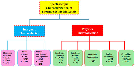
Figure 3.
Various characterization approaches for inorganic and polymer (specifically PEDOT:PSS) TE materials.
2. Spectroscopies and Microscopy Techniques of Inorganic TE Materials
Inorganic TE materials, often semi-conductors, generally exhibit higher TE performance; however, they are more expensive and less flexible [130,132]. Inorganic materials—including chalcogenides (e.g., SnSe, PbTe, Bi2Te3) [133,134], Zintl phase compounds [135,136], skutterudites, clathrates [137], and oxides—have shown significant promise as TE materials [122,132].
The fundamental mechanisms that contribute to the boosted TE performance of inorganic materials are elucidated by using different spectroscopy characterizations, including EDX, UV−Vis spectroscopy, XPS, XRD, RS, NMR, and EELS. The general data interpretation guidelines for inorganic TE materials are explained in the sections below.
2.1. Electronic Structure Characterization
2.1.1. EDX Spectroscopy
Characterization of TE materials using EDX spectroscopy is pivotal for understanding their microstructural and electronic properties. EDX, often combined with scanning electron microscopy (SEM), allows for the analysis of local carrier concentration and band alignment, which are crucial for optimizing TE performance. This technique can effectively assess the band diagram and estimate band offsets in multi-phase materials—enhancing the filtering of undesired charge carriers [138]. As can be seen from Figure 4A, it also provides detailed elemental composition and distribution data essential for optimizing their performance. The paper utilizes SEM with EDX to characterize multi-phase TE materials, assessing local carrier concentration and band alignment, which are crucial for optimizing TE performance in magnesium silicide-based composites [139]. According to Cha et al. [140], the characteristic SEM picture and its corresponding elemental maps obtained by using EDS were recorded on the polished surface of the spark plasma sintering (SPS) processed specimen; the Sn precipitate was seemingly invisible in the SEM-EDS detection limit (Figure 4B), contrary to the result for the specimen that was subjected to further ball milling and annealing (Figure 4D). These results showed that isolated Sn would be better pulverized and homogenously distributed by the ball milling process.
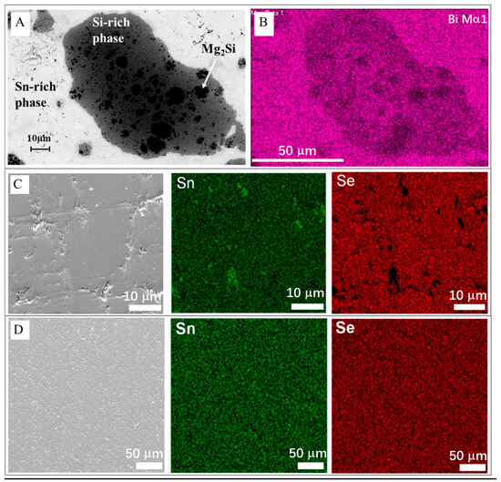
Figure 4.
(A). Backscattered electron image and (B) corresponding EDX mapping for (0.5)Mg2Sn/(0.5)Mg2Si0.98Bi0.02 composite. Adapted with permission from ref. [139] Copyright 2023, Elsevier. (C). SEM image and EDX elemental mapping of Sn and Se for Sn0.90Pb0.15Se0.95Cl0.05 melt-synthesized sample, showing Sn precipitate. (D). SEM image and EDX elemental mapping of Sn Se subject to melting, further ball milling, and annealing, showing uniform element distribution. Adapted with permission from ref. [140] Copyright 2019, American Chemical Society.
2.1.2. UV−Vis Spectroscopy
UV−Vis spectroscopy serves as a fundamental instrument for probing optical properties and electronic band structure of TE semi-conductors, measuring absorption, reflection, or transmission of light in the ultraviolet and visible electromagnetic spectrum regions [141,142]. The absorption edge value in the UV-Vis spectrum directly correlates with the material’s optical bandgap, a critical parameter influencing carrier concentration and effective mass, thereby impacting σ and S [37]. For instance, according to Rashad et al. [143], the absorption spectra of Bi2Te3 samples were analyzed by using a UV−Vis spectrophotometer at room temperature, as indicated in Figure 5A (left side). As can be observed in Figure 5A (left side), the absorption spectrum for the compound nanostructures showed absorption peaks for all specimens—including STNaPv−Bi2Te3, STPv−Bi2Te3, ST NaEd−Bi2Te3, STEd−Bi2Te3, and ST−Bi2Te3 at 284, 279, 280, 278.8, and 278 nm, respectively. The peaks were shifted/moved from 278 nm to 284 nm, which showed the impact of the nanostructure morphology and size. In addition, this redshift showed a reduction in Eg, hence raising the size of the particle. Normally, the two absorption peaks between 900 nm and 1100 nm in the IR region showed that the nano-powder of Bi2Te3 possessed the ability of thermal energy absorption from IR, as illustrated in Figure 5A (left side). In addition, Tauc plots derived from UV−Vis data enable the determination of direct or indirect bandgaps with high precision [144,145]. The energy of the bandgap or optical bandgap was determined for all specimens by using Tauc’s equation, as described by αhν = A(hν − Eg)n [146,147], where A is an energy-independent constant, α is the absorption coefficient, and n = 1/2 and 2 for indirect and direct transitions, respectively. The (αhν)2 changes with respect to E (hν) for various Bi2Te3 specimens, and the extrapolation of a straight line to intersect through the E-axis is portrayed in Figure 5A (right side). It can be easily observed that the bandgap type (direct) for these materials resulted from transitions produced by electrons, indicating these materials include solely the electrons between the conduction and valence bands with no interaction in the lattice [143].
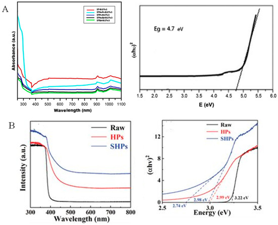
Figure 5.
(A). UV−Vis spectra for Bi2Te3 with various sample syntheses (left side) and corresponding Tauc sketches for the determination of bandgap (right side). Adapted with permission from ref. [143] Copyright 2018, Taylor & Francis. (B). UV−Vis absorption spectra (left side) and Tauc plot for determination of bandgap for sample ZnO-based TE materials (right side). Adapted with permission from ref. [142] Copyright 2024, Wiley.
In another study, UV−Vis spectroscopy was employed to elucidate the impact of Ov caused by specific high-pressure synthesis (SHPs) on the ZnO band structure and was applied to reflect the bandgap change. As portrayed in Figure 5B (right side), the bandgap of 3.22 eV of the raw specimen (between the conduction band minimum (CBM) and the valence band maximum (VBM)) was estimated using Tauc sketch from the UV−Vis absorption spectrum, as presented in Figure 5B (left side); the high-pressure synthesis (HPs) and SHPs resulted in decreased bandgaps of, respectively, 2.99 eV and 2.98 eV. Moreover, for the SHPs specimen, there was another abrupt transformation in the absorption spectra at the longer wavelength, as depicted in Figure 5B (left side), resulting in a tail at 2.74 eV, as portrayed in Figure 5B (right side). Therefore, it is judicious that the tail at 2.74 eV can be attributed to the deep impurity states induced by Ovs, i.e., from the CBM level to the Ovs level [142].
2.1.3. XPS
XPS provides surface-sensitive analysis of elemental composition, chemical states, and electronic structure of topmost layers—crucial for understanding surface phenomena affecting TE device performance [148,149]. XPS was utilized to analyze the chemical states and composition of the AZO thin films. XPS measurements were carried out by a PHI−5400 X-ray photoemission spectrometer with a monochromatic Mg Kα (1253.6 eV) radiation source. Core-level binding energy (B.E) shifts reveal information about chemical bonding and oxidation states—particularly important for air-stable TE materials [131]. Recent developments in hard X-ray photoelectron spectroscopy (HAXPES) enable bulk-sensitive electronic structure analysis—bridging bulk and surface property relationships [150,151]. Angle-resolved XPS (ARXPS) provides depth-profiling capabilities essential for understanding interfacial effects and compositional gradients [152,153].
XPS chemical shift analysis enables quantitative assessment of dopant segregation and incorporation phenomena [154,155]. High-resolution XPS studies have revealed preferential dopant segregation at grain boundaries, significantly impacting electrical transport properties [156]. Ultraviolet photoelectron spectroscopy (UPS) complements XPS by probing valence band electronic structure and work function, critical parameters for understanding carrier injection and extraction in TE devices [157,158]. As illustrated in Figure 6, the combined XPS/UPS analysis provides comprehensive electronic structure characterization from core levels to valence band edge [158,159,160]. For instance, the oxidation states of each constituent element in BiCuSeO have thus far been established to be Se2−, Bi3+, O2, and Cu1+ according to the necessity of the overall level of charge neutrality. Presumably, BiCuSeO is not a characteristic ionic compound, and therefore, the oxidation states of the elements have not been clearly defined. As a result, the authors performed XPS tests to verify the oxidation states. Despite a small quantity of Bi2+ being found, most of the Bi was certainly in the 3+ state within the BiCuSeO (undoped), as portrayed in Figure 6(Ba), whereby a smaller peak at the low-B.E side for the Bi3+ peak was observed. Within the Ca-doped specimens, no Bi2+ was evidently seen. Instead, a new peak appeared on the high-B.E side of the Bi3+ peak (see Figure 6(Bb)), showing some Bi ions with a higher oxidation state, apparently Bi4+. On the other hand, calcium (Ca) possesses a stable 2+ oxidation state—which is certainly verified in Figure 6(Bc)—whereby the 2p1/2 and 2p3/2 doublets with the B.E spacing of ca. 3.66 eV and intensity ratio of ∼1:2 are always seen within multiple Ca compounds, including CaO, CaSO4, and CaCO3. Consequently, one of the mechanisms for charge compensation in the doping of Ca2+ was discovered through the oxidation of a certain Bi3+ into Bi4+.
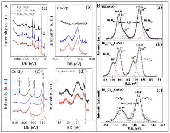
Figure 6.
(A). (a) XPS spectra for Bi2Sr2−xCaxCo2Oy, where x = 0.5, 0.3, and 0 for red, blue, and black lines, respectively. (b) High-resolution XPS spectrum of the Ca-2p core level for x = 0.5, 0.3, and 0 for red, blue, and black lines, respectively. (c) High-resolution XPS of the Co-2p core level for x = 0.5, 0.3, and 0 for red, blue, and black lines, respectively. (d) XPS valence band spectra of Bi2Sr2−xCaxCo2Oy for x = 0.5 (red line) and 0.3 (black line) samples. Adapted with permission from ref. [161] Copyright 2023, MDPI. (B). (a,b) XPS spectra for BiCuSeO at the B.E range in Bi 4f. The smaller open circles denote the estimated experimental points; the solid line represents the total of all the peak fittings portrayed by the dashed lines. (c) XPS spectrum of the Ca (2p). The smaller open circles denote the estimated experimental points; the solid line represents the total of all the peak fittings portrayed by the dashed lines. Adapted with permission from ref. [148] Copyright 2016, Elsevier.
2.2. Phase Analysis
2.2.1. RS
RS provides complementary vibrational analysis to IR, probing different selection rule-allowed phonon modes and offering unique insights into crystal symmetry, stress states, and defect structures [162,163]. RS provides characteristic phonon mode fingerprints, enabling material identification and quality assessment [164,165,166]. Peak positions, widths, and intensities reveal structural distortions, phase transitions, and doping effects on lattice vibrations [163,167]. Temperature-dependent Raman studies reveal anharmonic behavior through frequency shifts and peak broadening, directly correlating with k properties [168,169]. Recent investigations on SnSe single crystals have demonstrated exceptionally strong anharmonicity, contributing to record-low k [170,171]. Structural disorder and defects manifest as Raman peak broadening, frequency shifts, or the appearance of disorder-induced modes [172,173]. Quantitative analysis of peak parameters enables defect concentration estimation and its impact on transport properties [174]. Raman peak position shifts provide sensitive measures of local strain within TE materials [175], as displayed in Figure 7. Micro-Raman mapping enables spatial strain distribution analysis, particularly valuable for understanding stress effects in TE devices [175,176]. Resonance RS—achieved by matching excitation energy to electronic transitions—provides enhanced sensitivity to specific phonon modes and information about electron–phonon coupling [15]. This technique has proven particularly valuable for studying topological insulator TE materials [177].
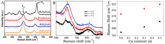
Figure 7.
(A). Raman spectra of the corresponding samples at 300 K. Adapted with permission from ref. [178] Copyright 2017, AIP Publishing. (B). Raman spectra of Bi2Sr2-xCaxCo2Oy with x = 0.5, 0.3, and 0 specimens at room temperature. (C). Expanded peak positions for the Raman band, which was marked by arrows for (B). Adapted with permission from ref. [161] Copyright 2023, MDPI.
For instance, to examine the lattice characteristics of Bi2[AE]2Co2Oy, Li et al. carried out the RS tests, as depicted in Figure 7A. For Bi2CaSrCo2Oy (BCSCO), Bi2Sr2Co2Oy (BSCO), and Bi2Ba2Co2Oy (BBCO)—there are two notable phonon peaks, i.e., the ~440 cm−1 (E1g) and ~615 cm−1 (A1g) modes—that denote the in-plane vibration and out-of-plane vibration of the oxygen atoms, respectively. The Raman spectrum of Bi2Ca2Co2Oy (BCCO) is different from the specimens, in which the peaks are observed at ~300 cm−1 and ~450 cm−1. It can be due to the relatively prominent Ca2+ and Ca−O layers in contrast to other specimens (BBCO, BSCO, and BCSCO) [178]. Raman spectra tests at room temperature were also performed in order to verify the incorporation of Ca within the Bi2Sr2Co2Oy (BSCO) lattice, as illustrated in Figure 7B. The Raman spectrum for Bi2Sr2−xCaxCo2Oy (for x = 0.5, 0.3, and 0) specimens from 500 cm−1 to 950 cm−1 at a temperature of 300 K was recorded (Figure 7B), showing two noticeable phonon peaks for all samples at ~618 and ~815 cm−1. The observed Raman peak at 618 cm−1 was allocated to A1g modes—signifying the out-of-plane vibrational mode for the oxygen atom. A small Raman peak position shift to the right was seen with the increase in the Ca content (Figure 7C). This observation can be elucidated by the rise in the Ca−O bond strength, with regard to the Sr−O bond [161].
2.2.2. NMR Spectroscopic
Solid-state NMR spectroscopy offers unique insights into dynamic processes, chemical bonding, and local atomic environments and is particularly valuable for understanding the incorporation of dopant and structural disorder effects [179,180]. Solid-state NMR can differentiate crystallographically distinct sites for specific nuclei (e.g., 207Pb, 119Sn, 77Se, and 125Te) within TE materials [181,182]. For instance, as can be seen in Figure 8A, the PbTe-rich part of the phase seen here comprises less sulfur compared to the nominal/theoretical composition; simulation studies yielded values of x Te-rich = 0.45 and 0.26 for nominal x = 0.5 and 0.3, respectively. In addition, excellent fits were discovered from observation of the model of spinodal decomposition, which was anticipated in this concentration area. This observation was in good agreement with the early stage of spinodal decomposition that was inferred from quenching the x = 0.5 specimen from the comprehensive scattering data analysis. A periodically modulated composition in space was generated by spinodal decomposition. This resulted in a local composition distribution; nevertheless, the major contributions were from the maximum and minimum values of x [182].
Quadrupolar coupling constants and chemical shifts offer detailed information about local symmetry, bond lengths, and coordination environments [183,184]. Recent multinuclear NMR observations on complex chalcogenides have shown subtle local structure variations influencing transport behaviors [185,186]. NMR chemical shift analysis enables estimation of dopant incorporation sites as well as mechanisms [187].
Recent studies on PbTe-based materials have employed 207Pb NMR to elucidate dopant-induced local structure modifications [188,189]. NMR spectroscopy can characterize and detect vacancies, point defects, and interstitial atoms—usually unresolvable by diffraction approaches [190,191]. Variable-temperature NMR offers insights into defect dynamics and their temperature dependence [191,192]. In skutterudite TE materials, NMR has been extensively employed to elucidate rattling dynamics and guest atom filling fractions within cage structures [193]. These tests directly correlate with phonon scattering boost and k reduction [194,195]. NMR relaxation rate analysis can give information about mobility and carrier dynamics, though challenging for excellent conductive TE materials [196,197]. Recent developments in high-field NMR have expanded applicability to more conductive systems [198,199,200].

Figure 8.
(A). 125Te NMR spectra for quenched PbTe1−x Sx (i.e., x = 0.5 and 0.3)—which were compared by bar graphs within the models by presuming incipient separation of phase. (a,b) Model supposing segregation of close to neat PbS—with insignificant NMR signal of 125Te. (c,d) Model of two components approaching the spinodal decomposition. The model indicated in (c,d) offers a more precise composition estimate—supposing that the spinodal decomposition during the early stages has generated inhomogeneous PbTe1−xSx alloying regions within the matrix. Adapted with permission from ref. [182] Copyright 2012, Wiley. (B). Dynamic in situ TE characterization for amorphous Ge (aGe)-based thin films: (a) radial profiles of selected area electron diffraction (SAED) patterns obtained at various stages through the experiment. Reflections that correspond to fcc Ge were indexed. (b) Low-loss electron energy loss (EEL) spectrum recorded at various stages indicated the Ge−M, aC, and Ge edge bulk plasmons. (c) Recorded voltage obtained by applying current for double sweeps as displayed by dashed lines (down) and solid lines (up) with a variation from blue color to red color through the rise in the value of current. The calculated values of resistance at the highest applied current were presented using black crosses for each sweep (secondary y-axis). Adapted with permission from ref. [201] Copyright 2025, Elsevier.
2.2.3. EELS
High-spatial-resolution EELS combined with TEM provides nanoscale elemental and electronic structure information crucial for understanding interfacial phenomena and nanostructure effects [202,203]. EELS enables determination of local bandgaps, plasmon excitations, and oxidation states at nanometer spatial resolution [204]. This capability proves invaluable for characterizing interfaces, grain boundaries, and nanostructures in TE materials [205,206]. EELS analysis for TE interfaces reveals electronic structure modifications, charge transfer phenomena, and local composition variations that affect transport properties [22,207]. Recent studies have demonstrated a correlation between interfacial electronic structure and enhanced S in nanostructured materials [131,208]—EELS compositional mapping provides detailed analysis of element distribution, segregation phenomena, and phase boundaries at nanoscale resolution [209,210]. This information can prove the crucial importance of understanding nanostructure stability and transport property optimization [211].
For instance, Hettler et al. [201] employed a dynamic in situ TE characterization by inducing thermovoltage in the crystallization engineering of an amorphous Ge thin film by the application of higher current densities. The SAED pattern radial profile is portrayed in Figure 8(Ba) with a blue line showing two broad peaks—which were centered close to 3 nm−1 and 5.4 nm−1. The lower-loss EEL spectra (i.e., blue line as presented in Figure 8(Bb)) verified the existence of both Ge, which was reflected through the bulk plasmon near the Ge−M edge and 16 eV, and amorphous C (aC), which was visible at 25 eV (i.e., in the bulk plasmon). After this unplanned initial crystallization, the authors employed a double current sweep in series by increasing the highest current up to 240 A, in order to continue the crystallization engineering process within a controlled condition. The sweeps are portrayed in Figure 8(Bc)—in which dashed and solid lines represent the down- and up-sweeps, respectively—and the colors were blue at first and changed to red with the rising of the highest current. The estimated value of resistance at the highest current for each sweep was sketched using black color crosses and was seen to remain constant (73 K) up to an employed current (I) of 13 A before decreasing owing to the increase in σ of the semi-conducting Ge and an induced Joule heating effect. Above an employed current of about 70 A, the down- and up-sweeps started to vary significantly, showing a sample configurational/structural modification that was induced by the electrical current. The authors mentioned that this alteration was connected to, initially, an entire size growth in the crystallization region and, secondly, a grain size growth in the central area.
2.3. Surface Morphology and Crystalline Structure Analysis
2.3.1. SEM
SEM is the fundamental characterization method in which the TE material surface is explored. For instance, Figure 9(Aa–Ac) displays field emission SEM (FESEM) pictures for the prepared Bi2Te3-Bi2Se3 composite fracture surface of specimens, which were hot-pressed at a temperature range of 623–673 K and 80 MPa within a vacuum. These pictures clearly showed that the grain size and density of the composite specimens were both enlarged with sintering temperature. It can be observed from Figure 9A that the grain size of specimens that were hot-pressed at 673 K (Figure 9(Ab,Ac)) is clearly larger compared to that of the specimen that was hot-pressed at 623 K (Figure 9(Aa)) [212]. Figure 9(Ba) shows an SEM picture of a drop-cast film for the crystalline Te nanorod passivated by PEDOT:PSS that was created into a smooth thin-film nanocomposite by using the solution-casting technique [109]. Figure 9(Bb) presents the SEM image of the cross-sections of the composite of CNT (5 wt.%) and polymer (poly(vinyl acetate) (PVAc) following the freeze-fracturing of the composites. The SEM picture with higher magnification is shown in Figure 9(Bc), which was a portion of the specimen in Figure 9(Bb) (i.e., portrayed with a yellow solid square) [213].
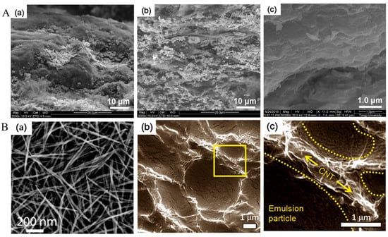
Figure 9.
(A). FESEM pictures of the fracture surface of the Bi2Te3-Bi2Se3 composite specimens that were hot-pressed at a temperature of (a) 623 K, and (b,c) 673 K and 80 MPa. Adapted with permission from ref. [212] Copyright 2011, Springer Nature (B). (a) SEM picture of a drop-cast PEDOT:PSS passivated crystalline Te nanorods thin film composite. Adapted with permission from ref. [109] Copyright 2010, American Chemical Society. (b) SEM pictures of the cross-sections of CNT (5 wt.%)—PVAc composites are indicated in panels b and c for freeze-fractured composites. The SEM image with higher magnification indicated in panel (c) is a part of the specimen in (b), as shown by a solid square with yellow color. It obviously indicated that CNTs (as shown with arrows), which are wrapped around particles at the emulsion (as shown with yellow dotted lines) instead of being homogenously blended. Adapted with permission from ref. [213] Copyright 2008, American Chemical Society.
2.3.2. TEM
TEM offers higher resolution as compared to that of SEM for better observations of TE materials. For instance, Figure 10A,B show the TEM pictures of the prepared Bi2Te3 nanopowders and PTH, indicating the differences in shape and particle size. It can be observed from Figure 10A that the prepared Bi2Te3 powders largely comprised nanosheets, with approximate sizes of 50 to 200 nm. The synthesized PTH powders were spherical with a mean diameter of approximately 200 nm (Figure 10B) [214]. Figure 10C presents TEM pictures of the crystalline Te nanorod, which was passivated using PEDOT:PSS [109].
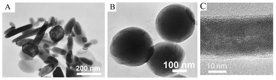
Figure 10.
(A). TEM pictures of the Bi2Te3 nanopowders manufactured through the hydrothermal synthesis approach; (B). TEM images of PTH synthesized through the chemical oxidative polymerization method. Adapted with permission from ref. [214] Copyright 2012, Springer. (C). TEM picture indicating the PEDOT:PSS passivated crystalline Te nanorod. Adapted with permission from ref. [109] Copyright 2010, American Chemical Society.
2.3.3. XRD
XRD remains indispensable for characterizing the crystal structure, phase purity, and microstructural features of inorganic TE materials [215,216]. XRD results/patterns provide unique crystallographic fingerprints, enabling identification of primary TE phases and secondary phase detection [217,218]. Phase purity critically influences TE performance, as secondary phases can severely degrade transport properties [219,220,221]. Advanced Rietveld refinement techniques enable quantitative phase analysis and precise structural parameter determination [222,223]. Recent developments in machine learning-assisted phase identification have accelerated the discovery of new TE phases [224,225,226]. Precise diffraction peak position analysis enables determination of lattice parameters and their evolution with composition, temperature, and doping level [227,228]. Vegard’s law analysis provides insights into solid solution formation limits and phase boundaries [229,230,231,232].
High-temperature XRD studies have revealed temperature-induced structural transitions, contributing to enhanced TE performance in materials like SnSe and GeTe [233,234,235]. Diffraction peak broadening analysis by the Scherrer equation provides crystallite size information, crucial for understanding nanostructuring effects on k reduction [236,237,238]. Warren–Averbach analysis enables the separation of size and strain broadening contributions [36,239]. Texture analysis through orientation of distribution function calculations reveals preferred crystallographic orientations impacting anisotropic transport properties [240,241]. While XRD cannot directly visualize point defects, systematic analysis of peak intensities, profile shapes, and diffuse scattering provides valuable defect information [207,242]. Advanced pair distribution function (PDF) analysis enables local structure characterization, complementing average structure information [243,244].
For instance, XRD results/patterns of (Sn1−xGex)Se for powders and SPS-pressed samples are presented in Figure 11(Aa–Ac) [216]. The authors showed that diffraction peaks can be well indexed to SnSe with the orthorhombic phase (Pnma space group, PDF #48-1224). The XRD results verified that all the (Sn1−xGex)Se samples were single-phase in the absence of any impurity. The anisotropic structures were seen in all samples sintered by SPS. The relative intensities of the two reflection peaks (111) and (400) were specifically diverse in the patterns of (b) and (c), indicating the inclination of grains growing along these planes. The SEM picture of Figure 11(Ad) indicates the freshly fractured surface morphologies of the specimens parallel to the direction of sintering for (Sn0.99 Ge0.01)Se. The pronounced layered structures were seen arranged along the parallel direction, indicating the grains were preferably reoriented into the disk plane through the sintering stage. Figure 11(Ba) shows the XRD results/patterns of the Sn0.99Na0.01Se-Ag8SnSe6 (Sn0.99Na0.01Se-STSe), SnSe-Ag8SnSe6 (SnSe-STSe), Sn0.98Ag0.01Na0.01Se, Sn0.99Na0.01Se, Sn0.99Ag0.01Se, and SnSe specimens [245]. The main peaks in the XRD results were indexed to the orthorhombic SnSe phase (JCPDF No. 014-0159) with a Pnma symmetry. Moreover, observable peaks pertinent to the orthorhombic β−Ag8SnSe6 (ICSD No. 95093, space group of Pmn21) were seen in the expanded XRD results/patterns of the SnSe−STSe and Sn0.99Na0.01Se−STSe specimens, as demonstrated in Figure 11(Bb).
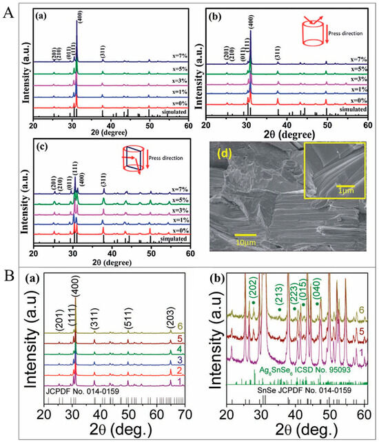
Figure 11.
(A). The XRD results/patterns of (Sn1−xGex)Se: (a) powders, (b) planes perpendicular, (c) planes parallel to the direction of SPS pressing, and (d) SEM pictures of the SPS-sintered fractured surfaces of (Sn0.99Ge0.01)Se bulk specimen parallel to the direction of the press. Adapted with permission from ref. [216] Copyright 2016, The Royal Society of Chemistry. (B). (a) Powder XRD patterns of SnSe (1), Sn0.99Ag0.01Se (2), Sn0.99Na0.01Se (3), Sn0.98Ag0.01Na0.01Se (4), SnSeAg8SnSe6 (SnSe-STSe) (5), and Sn0.99Na0.01Se-Ag8SnSe6 (Sn0.99Na0.01Se-STSe) (6) specimens. (b) Expanded XRD results/patterns of SnSe, SnSe-STSe, and Sn0.99Na0.01Se-STSe specimens showing the presence of Ag8SnSe6 as a second phase. Adapted with permission from ref. [245]. Copyright 2018, Wiley.
3. Spectroscopic and Microscopic Approaches Applied to Polymer TE Materials
Conducting polymers—also known as synthetic metals because they exhibit properties of metals, or plastics, or semi-conductors—have been extensively studied due to their high σ, low k, low density, advanced portability, and flexibility since they were first discovered in 1977 [246,247]. Organic TE materials—including polycarbazole, polyazulene, polythiophenes, poly(phenylene vinylenes) (PPV), polyacetylene (PA), polypyrrole (PPy), polyaniline (PANI), and their composites with carbon nanostructures or inorganic materials—have been extensively investigated, and all these materials possess π-conjugated structures [248,249,250,251,252,253,254,255,256]. The S and σ parameters of organic TE materials are strongly interdependent. For instance, Russ et al. investigated the change in the S and PF for a variety of organic n-and p-type TE materials and composites with regard to their σ (Figure 12). The authors established that S reduces with the increase in σ via the relation S ∝ σ−1/4, while PF rises with the increase in σ via the empirical relationship PF = σS2 ∝ σ1/2 [257]. Amongst all those usually employed conducting polymers, PEDOT:PSS has attracted increasing interest from both academia and industry owing to its superior σ and S, low k, and solution processability, as well as stability in the air amongst all these organic TE materials. PEDOT is doped by PSS to form dispersion in water and is broadly employed in the field of solar cells and light-emitting diodes, as well as other optical devices [258]. One of the best characteristics of PEDOT:PSS is that n can be controlled without altering S too much through the doping process. Also, PEDOT:PSS is mainly commercially available—and it can be fabricated on a large scale—which makes it a good candidate material for TE applications [259]. Hence, organic-based TE materials, particularly PEDOT:PSS, are promising candidates for use in the field of energy conversion materials in the future. Various treatment approaches have been established to enhance the TE performance/properties of PEDOT:PSS solution or films, by employing various acids, solvents, reducing agents, and ionic liquids, as summarized in Table 1. The enhancement is mainly ascribed to the enhanced σ or S [2,62,65,72,260,261]. However, pre- or post-treatment processing, which involves toxic materials to attain such enhanced TE performance, with unsatisfactory/poorer mechanical flexibility, usually limits the scale-up to industrial production. Therefore, discovering facile methods for the pre- or post-treatment of PEDOT:PSS is crucial, with particular emphasis on achieving chemical/mechanical robustness. There has also been little agreement about the origin and main mechanism responsible for PEDOT:PSS TE performance improvement until now. Hence, further work/research is essential to fully comprehend the fundamental mechanisms of these pre- or post-treatment methods, in order to optimize the TE behaviors/recital of PEDOT:PSS. Herein, in the sections below, we discuss the recent TE characterization techniques that have already been applied to study the mechanism of the boosted TE performance/behaviors of PEDOT:PSS films treated by numerous pre- or post-treatment approaches (as summarized in Table 1) and the general data interpretation guidelines for PEDOT:PSS TE materials.
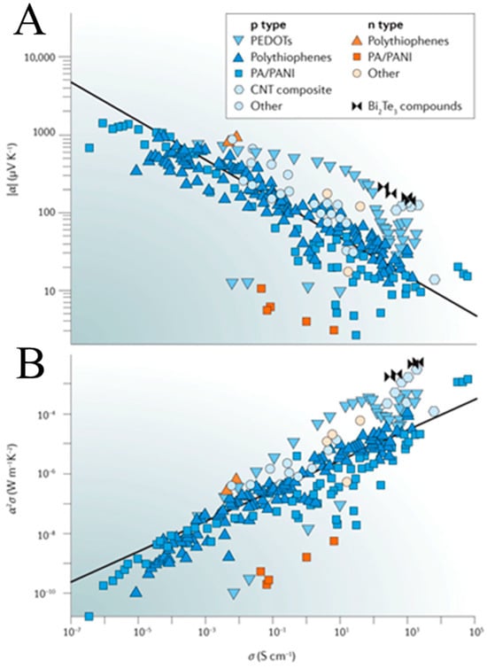
Figure 12.
The changes of (A) S and (B) PF with respect to the σ of organic and composite/hybrid TE materials. Adapted with permission from ref. [257]. Copyright 2016, Nature.
3.1. Electronic Structure
3.1.1. UV−Vis−NIR Spectroscopy
To understand the mechanism of the boosted TE behaviors of PEDOT:PSS films, the untreated and treated PEDOT:PSS films were characterized by employing UV-Vis-NIR spectroscopy. For instance, UV−Vis−NIR spectra for the pristine and sequential formamide (F), sodium formaldehyde sulfoxylate (SFS), and 1−butyl−3−methylimidazolium bis(trifluoromethanesulfonyl) amide (BMIM−TFSI)-treated PEDOT:PSS films are shown in Figure 13A. The absorption peak band detected at ca. 225 nm was mainly ascribed to the PSS. The reduced intensity of the absorption peak band at ca. 225 nm for PEDOT:PSS films indicates the removal of some PSSH chains for the treated PEDOT:PSS films. Compared with the F-PEDOT:PSS spectra—which indicated a notable intensity decrease at ca. 225 nm—the spectra of SFS−F−PEDOT:PSS as well as BMIM-TFSI-SFS-F-PEDOT:PSS almost did not change, like other treatments [262], showing that treatment with F efficiently detached PSSH, leading to a rise in σ compared to the untreated PEDOT:PSS film [263]. In another study, Luo et al. employed UV−Vis absorption spectra to examine the interaction of a mixture of DMSO and 1−ethyl−3−methylimidazolium tetrafluoroborate (EMIMBF4) with PEDOT:PSS thin films (Figure 13B). Nevertheless, the PEDOT/PSS ratio for films treated by DMSO/EMIMBF4 was not clearly defined owing to the signal convergence [264]. Figure 13C also displays the UV-Vis absorption spectrum of acid-treated PEDOT:PSS films (PA) and acid and then rhodamine 101 (R101)-treated PEDOT:PSS films (PRA). The UV−Vis absorbance spectrum indicates the transformation of electrons from R101 into PEDOT:PSS (Figure 13C). The absorption peak band close to 900 nm is assigned to the polaron, while the absorption close to 600 nm is ascribed to the neutral state in PEDOT. The polaron peak band becomes more notable for PRA compared to PA, which is not owing to the R101 absorption [83]. Figure 13D displays the UV−Vis−NIR spectrum of the untreated/pristine, benzenesulfonic acid (BSA)-doped, and DMSO-treated, as well as hydrazine (HZ)-treated PEDOT:PSS films. Typically, PEDOT chains possess three oxidation states—including neutral, polaron, and bipolaron states—that resemble the absorption peaks at 600 nm, 900 nm, and 1400 nm, respectively. As displayed in Figure 13D, there was no noticeable absorption peak band in the 450 nm-to-1100 nm range in pristine/untreated, BSA-doped, and DMSO-treated films. Nevertheless, following dedoping by solutions of HZ, stronger absorption peak bands were observed at ca. 600 nm and ca. 900 nm. Such a shift showed a transformation from the bipolaron into polaron and neutral states following treatment with HZ [82]. Figure 13E shows the UV−Vis spectrum within the range of 400 to 1100 nm. As presented in the spectra, the pristine PEDOT:PSS film showed a wide absorption within the near-infrared region, showing the major role of PEDOT2+. While referring to the deep eutectic solvents (DESs) and choline chloride (ChCl)-treated film spectrum, the existence of ChCl introduced a polaron absorption near 900 nm, indicating the PEDOT chains dedoping from bipolaron state to polaron state. Comparatively, no detectable conversion was observed in the spectra of PEDOT:PSS film with ethylene glycol (EG) post-treatment [265].
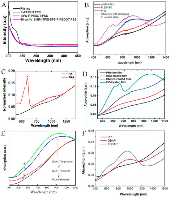
Figure 13.
(A). UV-Vis spectrum for the PEDOT:PSS (pristine), F-PEDOT:PSS, SFS−F−PEDOT:PSS, and BMIM−TFSI−SFS−F−PEDOT:PSS films. Adapted with permission from ref. [263] Copyright 2020, Frontiers. (B) UV−Vis spectrum of PEDOT:PSS films with various fabrication circumstances. Adapted with permission from ref. [264] Copyright 2013, The Royal Society of Chemistry. (C) UV−Vis absorbance spectra of PA and PAR films [83] Copyright 2023, Wiley. (D) UV-Vis-NIR spectrum for the untreated PEDOT:PSS, BSA-doped, DMSO-treated, and HZ-treated PEDOT:PSS films. Adapted with permission from ref. [82] Copyright 2018, Wiley. (E). UV−Vis spectrum of (d) pristine/untreated and after post-treated with (c) EG, (b) ChCl, and (a) DES. Adapted with permission from ref. [265] Copyright 2015, Wiley. (F) Vis−NIR spectrum of PP, DBAP, and TDBAP. Adapted with permission from ref. [77] Copyright 2025, Wiley.
More recently, Chen et al. [77] reported an enhanced PEDOT:PSS TE by treatment with tetrathiafulvalene (TTF). Figure 13F shows the Vis−NIR spectra for PEDOT:PSS (PP), - DBAP (acid and then base−DMSO) and acid–base–DMSO–tetrathiafulvalene (TDBAP) films. The absorption bands at 193 nm and 225 nm were mainly attributed to the benzene ring regions of rich PSS− or PSSH. The intensities of the two absorption peak bands dropped after the acid post-treatment as a result of the phase separation of the insulating PSSH shell from PEDOT:PSS. There was an apparent reduction in the intensity of the two absorption peak bands following post-treatment by TTF solution. This cannot be attributed to the TTF absorption. Apparently, TTF—as a weak reducing agent—may barely dedope DBAP. TTF comes to be TTF+ after the reduction, and then TTF+ and PSS− are rinsed away from PEDOT:PSS. In addition, some TTF molecules stayed in PEDOT:PSS, and they can possess a specific interaction with the conjugated PEDOT chains. The three bands at 1200, 900, and 600 nm were assigned to the neutral, polaron, and bipolaron states, respectively. The polaron band of DBAP was slightly weaker compared to the BAP film. This can be attributed to the rise in crystallinity, which can delocalize the holes and hence lower the values of the polaron density. After post-treatment with a solution of TTF with DBAP, a shoulder appears at approximately 600 nm. This was not because of the absorption of TTF, as TTF possesses no absorption within this range. The polaron absorption band of TDBAP is also remarkably stronger compared to that of DBAP. These conversions can be attributed to the slight reduction in PEDOT by using TTF. Furthermore, the peak position of the polar band was blue-shifted after the post-treatment with the TTF solution. It appeared at 1004 nm for DBAP and was shifted to 956 nm for TDBAP.
Generally, the explanation of the UV-Vis-NIR spectrum of PEDOT:PSS has been amended. For instance, Zozoulenko et al. [266] have interpreted according to the density functional theory calculations that the absorption peak at ca. 700−1000 nm may be ascribed to both polaronic and bipolaronic states, and that the peak in the NIR range may be attributed to polarons as well as bipolaron states originating from a higher oxidation state of PEDOT. Nevertheless, the summaries made here remain valid in light of these new views/explanations, since the decreasing/increasing tendency in the range of Vis−NIR helps the change from a higher to a lower oxidation level/state following post-treatment by solution.
3.1.2. UPS
According to Mott’s theory, S is proportional to the slope of the electronic density of states (DOS) at the Fermi energy level [6,267]. The UPS study can be employed to scrutinize the transformation in slope. For instance, Wang et al. reported the UPS spectra of BSA and HZ-treated PEDOT:PSS films (Figure 14A). The authors showed that the HZ-treated film exhibited a somewhat lower work function (Φ) than that of the BSA-treated film. Based on band theory analysis, the Fermi level (EF) of PEDOT:PSS position was shifted deep into the interior of the valence band for the heavily doped PEDOT films. A lower value of Φ suggested the moving of EF to the top of the deep valence band, in which DOS varied abruptly; therefore, the S was boosted for HZ-treated PEDOT films [82].
Another study by Yemata and colleagues reported that, along with increasing the TE properties of the PEDOT:PSS films, the ionic liquid (IL) treatment of the films affected other behaviors of PEDOT:PSS films, which are relevant to the operation of the device, like Φ. They showed that UPS was a key method to measure the surface Φ by determining the secondary-electron cut-off (Ec). The impact of valence band and Φ on the pristine and treated PEDOT:PSS thin films was estimated by applying UPS tests (Figure 14B) [263]. In fact, based on the UPS tests, the Φ can be estimated using Φ = hv – Ec, where hv is the photon energy (hv ≤ 21.2 eV) of the UPS light source, and the Ec of the spectral width is found from the energy gap between the Fermi edge and inelastic secondary-electron emission (SEE) cut-off [268,269]. The authors discovered that treatment of the film by IL resulted in a reduction in the Φ from 4.7 eV to 4.4 eV (Figure 14B). They also indicated that Φ ranging from 4.7 eV to 5.4 eV was reported in the literature for PEDOT:PSS thin films [270,271], which is in good agreement with the results exhibited in Figure 14B. The variation in the value of Φ is suggested to be associated with the top-layer differences, which may contain an excess of the PSS shell [269,272]. The top layer with rich PSS chains can be altered using the inclusion of higher-boiling solvents [273] and other processing conditions [274].
In the more recent method, the Φ of the sequential acid (H2SO4), base (NaOH), DMSO, and tetrathiafulvalene (TTF)-treated PEDOT:PSS films was investigated by UPS (Figure 14C,D). As exhibited in Figure 14C,D, treatment with DMSO or TTF solution shifted the cut-off edge of the spectra imaged with the UPS. The ϕ was determined in terms of the binding cut-off energy (E cut-off) and the photon energy (21.2 eV) using a cut-off of ϕ = 21.2-E. The ϕ of PP was 4.78 eV, and it decreased to 4.47 eV for BAP. This can arise by the dedoping of PEDOT:PSS using NaOH, which shifted up the Fermi level. The ϕ of DBAP was also 4.57 eV for DBAP, and it reduced to 4.33 eV for TDBAP, suggesting the shifting up of the Fermi level by treatment with TTF solution [77].
Guan et al. also employed UPS to study the Φ for MXene (Ti3C2Tx) (two-dimensional (2D) n-type material), which was mixed with PEDOT:PSS. As displayed in Figure 14E, the Φ values of MXene and PEDOT:PSS were 4.61 and 4.84 eV, respectively. They showed that the PEDOT:PSS Fermi level was lower compared to that of MXene. Hence, the electrons close to the MXene Fermi level were transferred from MXene to PEDOT:PSS until the Fermi levels were aligned. As both PEDOT:PSS and MXene possess a metallic electronic configuration, the transfer of charge can occur only in a narrow range. The authors concluded that this cannot be observed through XPS, RS, or UV−Vis absorbance spectroscopy [275].
Kim et al. applied UPS spectra to investigate the effect of polar solvent vapor annealing (PSVA) treatment in the Φ values for PEDOT:PSS/Bi2Te3 NWs composite film by employing DMSO as a polar solvent (Figure 14F). The treatment by PSVA enables altering the Φ value of the PEDOT:PSS and tuning the barrier energy between Bi2Te3 NWs and PEDOT:PSS [276]. The untreated PEDOT:PSS film and the PSVA-treated PEDOT:PSS films (shorter duration) showed higher Φ compared to that of Bi2Te3 NWs (Φ = 4.83 eV), whereas all the other specimens—including PSVA-treated films (long duration)—showed lower Φ compared to that of Bi2Te3 NWs, confirming the successful tuning of the Φ of PDOT:PSS by simply changing the PSVA duration [276].

Figure 14.
(A). UPS spectra for HZ (red) and BSA (black)-treated PEDOT:PSS films. Here, the inset sketch is the DOS for BSA- and HZ-treated PEDOT:PSS. Adapted with permission from ref. [82] Copyright 2018, Wiley. (B). UPS spectra of untreated, SFS−F−PEDOT:PSS and BMIM−TFSI−SFS−F−PEDOT:PSS films obtained by employing He I photon (21.22 eV): (#1) untreated, (#2) SFS-F-PEDOT:PSS, and (#3) BMIM−TFSI−SFS−F−PEDOT:PSS. Adapted with permission from ref. [263] Copyright 2020, Frontiers. (C). The cut-off edge and (D) Fermi level of the UPS spectra for PP, BAP, DBAP, and TDBAP films. Adapted with permission from ref. [77] Copyright 2025, Wiley. (E). UPS spectra of pure PEDOT:PSS and neat MXene. Adapted with permission from ref. [275] Copyright 2020, American Chemical Society. (F). UPS observations for pure Bi2Te3 NWs or powder and composite films based on short or long PSVA duration. Adapted with permission from ref. [276] Copyright 2020, Elsevier.
3.2. Functional Groups Analysis
3.2.1. ATR-FTIR Spectroscopy
ATR-FTIR spectroscopy can be employed to examine the impact of the various treatments on the chemical structures of PEDOT:PSS films. For instance, Alemu et al. employed ATR-FTIR to confirm the washing away of PSS chains for methanol (MeOH)-treated PEDOT:PSS film. After PEDOT:PSS film treatment through the dipping technique, the solution of MeOH was vaporized to increase the concentration of the removed PSS, and the ATR-FTIR tests were performed by dropping the MeOH on the infrared (IR) cell. Figure 15A shows the IR spectrum for a solution of MeOH obtained after MeOH vaporization—and it exhibited a characteristic PSSH spectrum. The absorbance peaks at 1005, 1035, 1125, and 1165 cm−1 were assigned to the sulfonate (SO3−) group vibration of the PSS. Moreover, the authors compared the PSSH spectrum of a commercial product of poly(sodium 4-styrenesulfonate) (PSSNa) (solid pellet)—and they observed a similar spectrum. This observation verified that the PSS chain was cleansed from the PEDOT:PSS film by treatment with MeOH without any chemical alteration. The authors also discussed that MeOH (with the highest dielectric constant (ε)) induced a charge screening effect between the PSS (negatively charged) and PEDOT (positively charged), resulting in Coulombic interaction reduction between them. This can lead to a significant phase segregation/separation of PEDOT and rich PSS on the nanometer scale, which can be depicted by segregation of the rich PSS phase. Further, the hydrophilic site of MeOH can easily dissolve and enhance the hydrophilic phase separation of PSS and then facilitate its wash away from the PREDOT:PSS film [277].
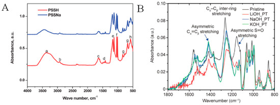
Figure 15.
(A). ATR-FTIR spectra of PSSH and PSSNa: (h). Ring in-plane deformation vibrations (615 cm−1 region); (g) out-of-plane C=H deformation vibrations (833 cm−1, 776 cm−1, and 670 cm−1 regions); (f) symmetric stretch of SO3− (1035 and 1005 cm−1regions); (e) SO3− asymmetric stretching vibrations (1165 and 1125 cm−1 regions); (d) C=C stretching vibrations (aromatic): 1410, 1450, 1495, and 1600 cm−1 regions); (c) bending vibrations of O−H (1640 cm−1 region); (b) alkyl C-H stretch vibration (2925 cm−1 region); and (a) stretching vibration of O-H (3700–2965 cm−1 regions). Adapted with permission from ref. [277] Copyright 2012, The Royal Society of Chemistry. (B). ATR-FTIR spectra for pristine, LiOH-, NaOH-, and KOH-treated PEDOT:PSS films. Adapted with permission from ref. [278] Copyright 2019, The authors.
Dong et al. also used ATR-FTIR spectrum for the analysis of PEDOT:PSS/DMSO films after post-treatment with various bases, including lithium hydroxide (LiOH), sodium hydroxide (NaOH), and potassium hydroxide (KOH), as shown in Figure 15B. The peak (i.e., at ca. 1155 cm−1) was greatly diminished after treatment with base. This signal was ascribed to an asymmetric stretching of PSS (S=O groups) in the form of a proton, showing the conversion of SO3H into SO3−. The peak at ca. 1524 cm−1 was assigned to the symmetrical stretching of (Cα=Cβ) thiophene ring, while the reduction in the peak ca. 1557 cm−1 (i.e., shifted to 1547 cm−1) was ascribed to the asymmetric stretching (Cα=Cβ) vibration, together indicating a conversion from a more quinoid structure to a more benzoid structure. In addition, a redshift from 1263 cm−1 to 1249 cm−1 (inter-ring Cα−Cα′ stretching) appeared—indicating that the Cα−Cα′ bond varied from a quinoid to benzoid structure. All these conversions can also support the dedoping process induced by base treatment. Notably, LiOH-treated PEDOT:PSS films showed a noticeable shoulder at ca. 1220 cm−1. This peak was assigned to the S=O groups that stretch from SO3−Li+, showing a strong interaction of Li+ and PSS− [278].
3.2.2. RS
In addition to UV−Vis−NIR spectra, RS can be employed to elucidate whether the various treatment techniques change the doping level of PEDOT:PSS films. Hence, to explain the influence of pre- or post-treatment on S, interest is directed to the structure PEDOT chains. It has already been verified that the oxidation level/state is vital for the S of PEDOT [279]. Acid/base chemistry, chemical dedoping engineering, and the electrochemical dedoping process can be employed for the transformation of the oxidation state/level [85,279]. It was also pointed out that upon the dedoping engineering, PEDOT can undergo three levels/states, as described in Scheme 1 [264]. The bipolaron level/state in PEDOT chains can be slowly dedoped into a polaron and then a neutral (doped) level. Through dedoping engineering, the σ is reduced whilst the S shows a boosting trend. These three PEDOT states exhibit absorbance at various wavelengths (PEDOT in the bipolaron level/state exhibits a broad absorbance in the near-infrared region (NIR, 700–900 nm) [280]; chains in the polaron state exhibit absorbance close to 900 nm [280]; and the neutral polymer PEDOT chains exhibit absorbance near 600 nm [280,281]).
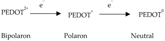
Scheme 1.
Different redox levels of PEDOT showing the transformation of PEDOT from bipolaron level to polaron, and then neutral level upon dedoping [264].
For instance, Luo et al. employed Raman spectra to elucidate the PEDOT:PSS films treated with various DMSO concentrations and a mixture of DMSO and EMIMBF4, as illustrated in Figure 16A. The absorbance of the untreated PEDOT:PSS film indicated a broad absorbance in the NIR region. There was no clear noticeable transformation in the DMSO-treated film. In contrast, EMIMBF4 treatment introduced a polaron absorption band, indicating the dedoping of PEDOT. In comparison with the partially dedoped PEDOT to the neutral state (600 to 700 nm referencing absorbance), EMIMBF4 only dedoped PEDOT from the bipolaron state to the polaron state. The authors confirmed that along with UV−Vis spectra and XPS analysis, it was confirmed that the EMIM cations dedoped the PEDOT and raised the density of polaron, as it was verified through the enhancement of S and reduction in σ. As displayed in Figure 16A, the spectra of DMSO-treated films appear like that of the untreated PEDOT:PSS film. Nevertheless, EMIMBF4-treated PEDOT:PSS films reveal a narrower band near 1436 cm−1, which was shifted to a smaller wavenumber region in contrast to the untreated PEDOT:PSS film. An additional peak was also observed at ca. 1510 cm−1. The alterations in Raman spectra verified the dedoping of PEDOT chains upon EMIMBF4 treatment [264].
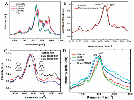
Figure 16.
(A). Raman spectra of pristine and treated PEDOT:PSS films by various post-treatment techniques. Reproduced with permission from ref. [264] Copyright 2013, The Royal Society of Chemistry. (B). The Raman spectra of the untreated and formamide-treated PEDOT:PSS (Dip + Drop)2 films. Reproduced with permission from ref. [70] Copyright 2017, Wiley. (C) Normalized Raman spectra of the pristine, BSA-doped, and CSA-doped PEDOT:PSS films. Adapted with permission from ref. [82] Copyright 2018, Wiley. (D) Raman spectra of the untreated, MeOH-, DMSO-, and TFMSA−MeOH-treated PEDOT:PSS films. Adapted with permission from ref. [282] Copyright 2018, The Royal Society of Chemistry.
In another study, Kyaw et al. employed RS along with Vis−NIR spectra to explore whether formamide-treated PEDOT:PSS films change the doping states of PEDOT:PSS. As shown in Figure 16B, the Raman peak near 1447 cm−1, which emerged from the five-membered thiophene ring (symmetric Cα=Cβ groups stretching), often shifted to a smaller wavenumber region along with a narrower bandwidth as the doping state diminished from the bipolaron level to the polaron state or neutral level. An insignificant shift in wavenumber (approximately 1 cm−1) and the bandwidth variation in the symmetric Cα=Cβ group stretching indicated that the formamide post-treatment did not alter the doping state noticeably, indeed accounting for a small variation in S value [70].
Wang et al. [82] also applied Raman spectra to study the transformation in untreated camphorsulfonic acid (CSA), as well as BSA-doped PEDOT:PSS films, as illustrated in Figure 16C. The authors pointed out that strong Raman bands were observed between 1400 cm−1 and 1500 cm−1, which were ascribed to the symmetric Cα=Cβ group stretching of PEDOT thiophene rings. The Raman peak appeared at 1441 cm−1 for the pristine film. The redshift in the Raman peak was detected for both CSA- and BSA-doped films, showing a resonant structure transformation from a benzoid to a quinoid configuration, as portrayed in the inset of Figure 16C. This conformational transformation provides the facilitation of long conjugated length and offers mobility of charge carriers. Another study by Wang and colleagues [282] applied Raman spectra to scrutinize untreated, MeOH, DMSO, and trifluoromethanesulfonic acid (TFMS)−MeOH-treated PEDOT:PSS films, as presented in Figure 16D. They showed that the MeOH and DMSO treatment did not cause a noteworthy transformation in its Raman band at about 1421 cm−1, which was ascribed to the stretching vibrations of the Cα=Cβ groups. On the other hand, the Raman band at 1421 cm−1 was downshifted to 1387 cm−1 by TFMS−MeOH treatments—switching from the benzoid configuration to the quinoid configuration in PEDOT chains.
3.3. Elemental Composition Analysis
XPS
The S2p XPS can be employed to investigate the impact of pre- or post-treatment and the interaction of pre- or post-treatments with PEDOT:PSS thin films. The loss of PSS chains from the PEDOT:PSS thin film following treatment can also be verified by using the XPS spectra of the PEDOT:PSS films. The two XPS bands with B.E between 166 eV and 172 eV are due to the S2p band of the sulfur atoms from PSS, while the two doublet XPS bands with B.E between 162 eV and 166 eV originate from the S2p band of the sulfur atoms from the PEDOT chain [283,284,285,286,287]. The S2p XPS band increased for PEDOT compared to that of PSS for PEDOT:PSS films following various treatments, suggesting the removal of rich PSS chains from the PEDOT:PSS films by the treatment.
For instance, Yemata et al. employed XPS spectra for formic acid-, sequential formic acid-, and HZ-treated PEDOT:PSS films. They noticed that the S2p intensity of the PEDOT boosted as compared to that of PSS due to the loss of the rich PSS chains, as illustrated in Figure 17A (i.e., deconvoluted S2p XPS spectra). The B.E values of 165.3 and 164.1 eV, belonging to S2p1/2 and S2p3/2, in the S(2p) core level spectra for PEDOT treated by formic acid were shifted to the low B.E at 164.9 eV and 163.7 eV, belonging to S2p1/2 and S2p3/2 for PEDOT treated by 0.15 wt.% HZ, correspondingly, indicating that the reduction in doping state/level following HZ treatment resulted in a decrease in B.E. These sulfur atoms in the PEDOT were shifted to low energy after the HZ treatment, confirming the dedoping of PEDOT [69].
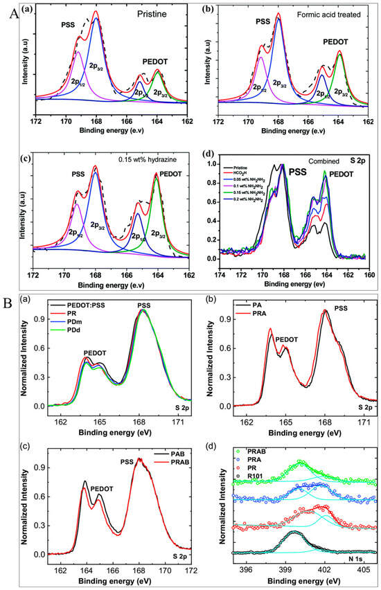
Figure 17.
(A). XPS spectrum of (a) untreated, (b) formic acid, (c) HZ (0.15 wt.%), and (d) normalized combination of untreated, formic acid-, HZ (various concentrations)-treated PEDOT:PSS films. Adapted with permission from ref. [69] Copyright 2020, The Royal Society of Chemistry. (B). S2p XPS spectra for (a) PEDOT:PSS films treated by different zwitterions; (b) PRA and PA; (c) PRAB and PAB; and (d) N1s XPS spectra of PRAB, PRA, PR, and R101. Adapted with permission from ref. [83] Copyright 2023, Wiley.
Li et al. [83] also employed the S2p XPS to investigate the impact of zwitterion treatment on PEDOT:PSS films and study the interaction of zwitterion with PEDOT:PSS thin films. The XPS spectra for PEDOT:PSS, PDOT:PSS/rhodamine 101 (R101) (PR), PEDOT:PSS/N−dodecyl−N,N−dimethyl−3−ammonio−1−propane-sulfonate (DDMAP) (PDd), and PEDOT:PSS/1−(N,N−dimethylcarbamoyl)−4−(2−sulfoethyl) pyridinium hydroxide (DMCSP) (PDm) thin films are portrayed in Figure 17(Ba). The zwitterions—especially R101—induced a remarkable redshift related to the S2p XPS band of PEDOT chains. For PEDOT:PSS, the S2p B.Es were 164.1 eV and 165 eV, and these BE values were shifted to 163.95 eV and 164.9 eV for PDm and 163.85 eV and 164.75 eV for PR. On the other hand, PDd did not cause the redshift related to the S2p B.Es. The redshifts in PDm and PR were ascribed to the electron transfer from DMCSP to PEDOT and R101 to PEDOT, respectively. These were also in good agreement with their π−π overlapping of PEDOT chains. The -R101 caused the redshift in the S2p XPS bands for PEDOT chains following acid treatment. As displayed in Figure 17(Bb), the XPS intensity of the S2p bands of PEDOT remarkably increased compared to that of PSS−, owing to the loss of rich PSS chain following the acid post-treatment, whereas the B.Es for PA were almost similar to that of the PEDOT:PSS film. For PRA films, the B.Es were shifted to 163.85 eV and 164.9 eV. Also, the occurrence of R101 induced the redshift related to the S2p XPS bands of PEDOT following the sequential acid and base treatment. Similarly, as shown in Figure 17(Bc), the B.Es were assigned to be 163.85 eV and 164.90 eV for PAB—and these B.E values were shifted to 163.8 eV and 164.85 eV for PRAB. Figure 17(Bd) exhibits the N1s spectra of XPS for PRAB, PRA, PR, and R101. The N1s spectra/bands for R101 were deconvoluted to a broad band spectrum at ca. 399.66 eV (i.e., arises because of the neutral N atom) and a small shoulder at about 401.54 eV (i.e., emerged from NH+ because of the transformation of a proton from the carboxylic group and the nitrogen atom) [69]. The minor N1s band spectra of XPS because of NH+ become significant for both PR and PRA; nevertheless, they become unremarkable for PRAB. The observations showed that the protonation of the R101 N atom occurs through an aqueous solution of PEDOT:PSS (i.e., ca. pH = 2) and the deprotonation through base treatment. Moreover, the major B.E for N1s spectra was blue-shifted for PRAB, PRA, and PR in contrast to that of pure R101. This blueshift in N1s B.E indicated the transfer of an electron from R101 into PEDOT, which is in good agreement with the redshift for S2p B.Es within PEDOT.
3.4. Surface Morphology Analysis
As discussed in the above sections, the spectroscopic studies and XPS tests, together with the diminished thickness, indicate the extraction of rich PSS chains, leading to a boosted PEDOT/PSS ratio in support of rich PEDOT (conductive) grains. Nevertheless, examining the increased TE performance for various pre- or post-treatments by different methods—with almost no reduction in the thickness of the film being observable—shows that the extraction of rich PSS chains alone cannot elucidate the excellent increase in the TE performance of PEDOT:PSS films. Hence, further investigations of the relationship among the morphology, structure, and TE behaviors of the untreated and pre/post-treated PEDOT:PSS films by different methods have to be performed using surface morphological characterization techniques such as AFM and SEM, as well as crystalline structure analysis approaches including XRD and GIWAXS.
3.4.1. AFM
AFM pictures can be taken to characterize the surface morphology before and after various treatments of PEDOT:PSS films, as the change in the AFM pictures can suggest the PEDOT:PSS polymer chains’ conformational transformation. In addition, information about the change in the AFM images can be extracted to elucidate the likely transformation within the morphology, as well as the correlation between TE properties and morphology. For instance, the morphologies of BMIM−TFSI−SFS−F−PEDOT:PSS, SFS−F−PEDOT:PSS, F−PEDOT:PSS, and untreated PEDOT:PSS were studied using AFM (Figure 18A). The treated films had highly non-uniform surfaces, increased particle size, and resulted in a more readily charge carrier transport that yielded an enhanced σ compared to that of the untreated PEDOT:PSS film. As shown in Figure 18(Aa,Ae), the pristine film did not display any apparent grains, showing that the PEDOT-rich chains were well-intermixed with the PSS-rich chains, and the soft shells (PSS-rich domains) typically covered the film. It has already been observed earlier that the treatment can result in strong phase segregation/separation between the rigid core (PEDOT-rich core) and the soft PSS-rich shell and reduction in PSS chains following various treatments of PEDOT:PSS films, leading to improved PEDOT-rich interconnected grains (Figure 18(Ab–Ah)) [264,288]. Following dedoping by ILs, the PEDOT-rich interconnected grains were boosted, leading to an improved σ compared to the untreated PEDOT:PSS film. This may partially address the mechanism for why treatment with ILs can improve PF with a negligible reduction in σ [263].
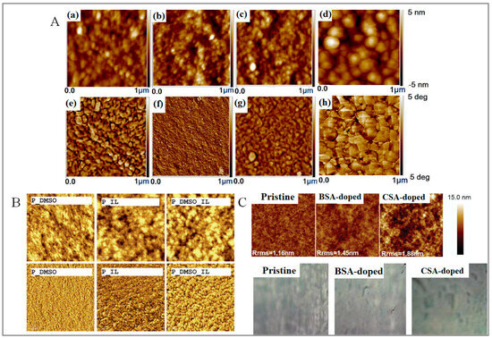
Figure 18.
(A). AFM images for IL−SFS−F−PEDOT:PSS, SFS−F−PEDOT:PSS, and untreated films. Height images: (a) pristine, (b) 0, (c) 100 mM SFS in water for SFS−F−PEDOT:PSS, and (d) BMIM−TFSI (40 vol.%) for IL−SFS−F−PEDOT:PSS films. Phase images: (e) pristine, (f) 0, (g) 100 mM SFS in water for SFS−F−PEDOT:PSS, and (h) BMIM−TFSI (40 vol.%) for IL−SFS−F−PEDOT:PSS films. The scanned area was 1 μm × 1 μm for each picture. Adapted with permission from ref. [263] Copyright 2020, Frontiers. (B). The AFM pictures of PEDOT:PSS films captured by different treatments. Height images (upper row) and phase images (lower row). The scanning area was 1 × 1 mm2. Adapted with permission from ref. [264] Copyright 2013, The Royal Society of Chemistry. (C). Upper row: AFM pictures of the untreated, BSA-doped, and CSA-doped PEDOT:PSS films. The picture size was 2 μm × 2 μm. Lower row: pictures of the untreated, BSA-doped, and CSA-doped PEDOT:PSS films obtained by the camera of the stylus profiler. Adapted with permission from ref. [82] Copyright 2018, Wiley.
Luo et al. also employed AFM to examine the possible morphology transformations and the correlation between the σ and morphology of the PEDOT:PSS film following various chemical treatments, as portrayed in Figure 18B. The DMSO-treated PEDOT:PSS film (P/DMSO) showed noticeable elongated grains, which can possibly be due to the loss of excess PSS chains from the film surface. The phase separation and depilation of excess PSS chains were also verified by the surface roughening of the film. The root-mean-square (rms) surface roughness was 1.36 nm, 2.00 nm, 1.28 nm, and 1.6 nm for the untreated, P/DMSO, EMIMBF4-treated PEDOT:PSS (P/IL), and sequential DMSO- and EMIMBF4-treated PEDOT:PSS (P/DMSO/IL) films, respectively. Correspondingly, phase segregation was also found for the P/IL film—and the grains were slightly elongated with short and circular PEDOT-rich grains. Similarly, elongated PEDOT-rich grains were obtained for P/DMSO films, and the subsequent EMIMBF4 treatment resulted in morphology transformation, and hence, circular and short PEDOT-rich grains were produced. The circular/short PEDOT-rich grains rendered the film with low surface roughness. In contrast to P/DMSO (with rms value of 2 nm), the decrease in surface roughness for P/DMSO/IL (with rms value of 1.64 nm) showed the likely reaction of EMIMBF4 with the PEDOT:PSS thin film that constrained the elongation of PEDOT-rich grains, resulting in circular and short PEDOT-rich grains [264].
Another study by Wang et al. reported the PEDOT:PSS film surface morphologies using various post-treatments (i.e., three specimens—including pristine, BSA-, and CSA-doped PEDOT:PSS thin films—were recorded and compared). As shown in Figure 18C (upper row), the untreated PEDOT:PSS film exhibited quite a smooth and uniform surface with an rms roughness value of 1.16 nm. Following BSA or CSA doping, the film becomes rougher with a larger domain size—and rms increased to 1.45 nm and 1.88 nm, respectively. Moreover, the authors recorded the film surface images by using a digital camera (Figure 18C, lower row). Hence, both the AFM pictures and the enhanced rms values suggested a phase segregation between PSS chains and PEDOT chains. These resulted in a PEDOT chain conformational transformation (i.e., from a coil-like configuration to a fiber structure), resulting in more contact points within PEDOT-rich chains for a better transport of charge carriers. It is fascinating to note that CSA-doped PEDOT:PSS films were rougher compared to BSA-doped PEDOT:PSS films, which could be connected to the CSA stereo configuration. These structures dominantly impede the electrical contact within the PEDOT-rich chains to some extent, which consequently influences carrier mobility [82].
3.4.2. SEM
SEM images can be employed to elucidate the surface morphologies [289], the cross-sectional morphologies [290], and the thicknesses (using an accelerating voltage of 20 kilo volt (kV)) [291] for the PEDOT:PSS films before or after various pre- and/or post-treatment techniques. For instance, SEM was applied to study the morphologies of the zwitterions such as rhodamine 101 (R101) and PEDOT:PSS polymer films. As shown by SEM images (Figure 19(Aa,Ab)), a rhodamine 101 (R101)-treated PEDOT:PSS(PR) thin film revealed an extremely smooth surface. There were no clear alterations that can be seen on the surface of the film following sequential/combination treatments of PR with acid and base (PRAB). The EDX pictures of sulfur (S) and nitrogen (N) illustrated that R101 was uniformly dispersed in/on PEDOT:PSS [83]. In another observation, as portrayed in Figure 19B, the cross-sectional SEM pictures of (I) untreated, (II) formamide (CH3NO), (III) CH3NO and then sulfuric acid (H2SO4) (CH3NO/H2SO4), and (IV) CH3NO/H2SO4 and then sodium borohydride (NaBH4) (CH3NO/H2SO4/NaBH4) post-treated PEDOT:PSS thin films revealed distinct morphological differences. The authors confirmed that there was film thickness reduction after CH3NO/H2SO4 treatment due to the depilation of excess-free PSS chains between their (100) planes. In addition, the H2SO4-treated specimen exhibited a microstructure with lamella stacking that spread along the whole cross-section. The formation of a well-ordered microstructure was attributed to the significant loss of rich PSS chains aggregating within metallic grains as insulating domains. In the absence of these insulator domains, the direct and efficient contact within metallic grains will allow charge carriers to move smoothly in the PEDOT:PSS thin film, resulting in high charge carrier mobility. Thereby, σ was significantly elevated without sacrifice of S. Further NaBH4 treatment did not create any noticeable alteration to the film microstructural composition/crystallinity [290].
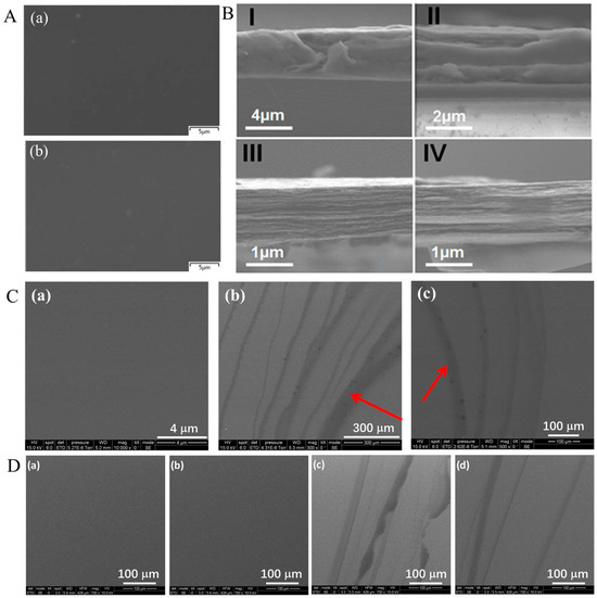
Figure 19.
(A). (a) Surface SEM of a PDOT:PSS/rhodamine 101 (R101) (PR) film. (b) Surface SEM of PRAB films. Adapted with permission from ref. [83] Copyright 2023, Wiley. (B). Cross-sectional SEM pictures of the following: (I) pristine, (II) CH3NO, (III) CH3NO−H2SO4, and (IV) CH3NO−H2SO4−NaBH4-treated PEDOT:PSS films. Adapted with permission from ref. [290] Copyright 2019, American Chemical Society. (C). SEM pictures of PEDOT:PSS thin films: (a) pristine, (b) 10 M formic acid, and (c) 26 M formic acid-treated films. The red arrow shows the segregated PSS. Adapted with permission from ref. [289] Copyright 2014, American Chemical Society. (D). SEM pictures of PEDOT:PSS films: (a) untreated; (b) treated by MeOH with the dipping technique; and (c,d) treated by MeOH with ther dropping technique. Adapted with permission from ref. [277] Copyright 2012, The Royal Society of Chemistry.
SEM images were also employed to characterize the morphologies of PEDOT:PSS films after formic acid treatment. As portrayed in Figure 19(Cb,Cc), the SEM pictures showed a segregated darker line, which was created after formic acid treatment and in good agreement with the SEM images obtained after MeOH treatment (see Figure 19D) [277]. These lines were attributed to insulator-rich PSS chains, and they were easily washed away after rinsing with distilled (DI) water. The film thickness was also decreased by about 20 nm to 25 nm following formic acid treatment. The authors also confirmed that there was almost no alteration in σ following DI water rinsing, but they sometimes observed certain film damage due to the high hydrophilic behavior of water. They also noted that PSS chain was only physically present on the surface of the film; nevertheless, functionally, the PSS chain was separated [289]. In another study, the same authors applied SEM to investigate the morphological change for MeOH-treated PEDOT:PSS. Figure 19D displays the SEM pictures of untreated and treated PEDOT:PSS films by using various approaches. The authors indicated that the darker lines observed in the SEM pictures in Figure 19(Dc,Dd) were the separated rich PSS chains which can be easily washed away by dipping in MeOH solution [277].
3.5. Crystalline Structure Analysis
3.5.1. GIWAXS
GIWAXS and grazing incidence small-angle X-ray scattering (GISAXS) have been broadly utilized for the investigation of functional materials with a specific emphasis on thin-film behaviors. GIWAXS data are usually 2D diffractograms comprising diffraction rings of various crystal planes, while GISAXS has a longer detector distance compared to that of GIWAXS. Both GIWAXS and GISAXS can be employed for nanostructured morphological characterization for the orientation and packing of conjugated polymers or aromatic molecules, nanoparticle assemblies, block copolymers, or nanocomposites. The convenient GIWAXS/GISAXS geometric scattering enables attaining complete information regarding the structure of thin films and elucidating specimens in well-described conditions, which can be controlled by coating processes or exposure to temperature, solvent drying, or vapor. In addition, with appropriate detectors and X-ray sources, information regarding phase transitions and ordering kinetics can be achieved down to the millisecond time scale [292,293].
GIWAXS plays a substantial role in investigating polymer PEDOT:PSS TE materials. The PEDOT:PSS thin-film structure can be characterized by GIWAXS in order to obtain more complete information regarding the packing of the PEDOT chains, where it is a very well-proven written protocol to study/characterize the crystalline/molecular structure of polymers lying at the surface or beneath a smooth layer [294,295,296,297]. The 2D GIWAXS with a larger area of mapping is an effective approach to elucidate molecular orientation and stacking. Since AFM tests are restricted to a slight local region of sampling and offer only the surface specific information, the inner PEDOT:PSS thin-film morphologies can be probed by employing GISAXS. Because of the geometry of grazing incidence, outstanding morphological information can be accessed and extracted from GISAXS [298,299]. It has already been verified that it is a vital technique for understanding and quantifying multiple property−structure relationships of thin films, which basically restrict the performance of optoelectronics. The crystalline regions of the sample films concerning structure and orientation can be probed and quantified by GIWAXS. In addition, GIWAXS enables the extraction of information about the ratio of PEDOT/PSS in the crystalline parts. Contrary to XPS, in which the information about the depth of excited electrons is restricted to the topmost surfaces/layers of the film—therefore making it a surface/layer-sensitive technique—GIWAXS measurements can provide guidance for probing and understanding the inner film configuration/structure in conjunction with a film specimen with large volume. This offers comprehensive information/data from the inner film with excellent statistics over a large specimen volume while being non-destructive [48,278,297,300]. In addition, the scattering geometry of GIWAXS and time-resolved GIWAXS is inherently feature-compatible with both under operando and in situ studies/setups (comprising standard protocols, ISOS) [301]. Hence, GIWAXS measurements have to be performed to detect how the various pre-/post-treatments change the overall PEDOT:PSS thin-film structure.
For instance, GIWAXS was used to characterize the semicrystalline structure of the PEDOT:PSS thin film before and after treatment, as presented in Figure 20(Aa–Ad). Corresponding to the surface morphology, the bulk film crystal structure had a significant transformation after the alkali/base solution post-treatments. Figure 20(Ae) displays the line profiles that rely on the full integration extracted from the pictures to attain a better visualization of the structural changes. The lower-angle part featured two clear peaks, including a distance (100) reflection that was situated at the lowest scattering vector (q) values, and the second peak was situated close to 0.48 Å−1. It was clear that the distance (100) peak placed close to q = 0.24 Å−1 for the untreated PEDOT:PSS film decreased in intensity following alkali/base post-treatment (i.e., a reduction in 37%, 20%, and 4% for KOH, NaOH, and LiOH, respectively) and shifted to 0.36, 0.32, and 0.28 Å−1 for the KOH, NaOH, and LiOH-treated PEDOT:PSS films, respectively. This implies that the adjacent (100) plane spacing gradually decreased from the untreated PEDOT:PSS film to the KOH-treated film (i.e., from 26.2 Å for the untreated to 22.4 Å for KOH, 19.6 Å for NaOH, and 17.4 Å for NaOH). The highly compact packing arrangements along the direction of [100] are contemplated to aid the transport of charge carriers within the crystal [302]. Notably, the peak intensity situated near the q value of 0.48 Å−1 along the qz direction displays a strong rise going from the untreated PEDOT:PSS film to the KOH-treated PEDOT:PSS film. There was also a clear peak (100) position shift by the alkali/base metal atom employed, while the peak position at a q value of 0.48 Å−1 was almost unchanged. In addition, the tendency of these two peak intensities was the opposite. The results indicate that the peak at a q value of 0.48 Å−1 was not linked to the second-order peak of (100). Here, two kinds of packing were observed, each one described by a diverse position of (100) peaks, including type I and type II crystals of PEDOT. Type I indicated doped PEDOT surrounded by the PSS chain and showed a large d spacing in the (100) direction, where a peak of (100) was placed toward smaller values of (q). Conversely, type II crystals of PEDOT exhibited slight or even no observable PSS within the crystals of PEDOT, resulting in a smaller (100) d spacing, where a peak of (100) was situated at high values. In this condition, the packing of PEDOT differs from largely type I to a blend of type I and II, based on the behaviors of the employed solution (i.e., basic/alkaline nature) (the estimated ratio of type I/type II was changed from 1.80 for untreated PEDOT:PSS to 1.31 for LiOH, 1.10 for NaOH, and 1.05 for KOH-treated PEDOT:PSS films. These observations showed the gradual loss of PSS chains by the doping process from the crystallites of the PEDOT chain, while the base/alkali treatment caused dedoping. In addition to the transformation in the packing of the PEDOT structure, the excess chains of PSS not directly linked with PEDOT also underwent transformation after post-treatment by base or alkali. The loss of peak of PSS showed a noticeable change from near 1.32 Å−1 for the untreated PEDOT:PSS film to 1.24 Å−1, 1.28 Å−1, and 1.28 Å−1 for LiOH-, NaOH-, and KOH-treated films, respectively. This result implies that the solutions of alkali base had an interaction with the PSS chain within the films, leading to a larger mean distance amongst the chains of PSS (from 4.8 Å for untreated to 5.1 Å, 4.9 Å, and 4.9 Å for LiOH-, NaOH-, and KOH-treated PEDOT:PSS films, respectively). Conversely, the peak of (010), which was linked to the ordering along the direction of PEDOT π–π stacking, was maintained at a similar ca. 1.83 Å−1 peak position, implying that the alkali post-treatment did not influence the inner molecular packing distance for PEDOT along the direction of π-π stacking. Nevertheless, the peak of (010) width transformation was seen following alkali post-treatment, as portrayed in Figure 20(Ae). The broadening of the detected peak of (010) was small for LiOH-treated PEDOT:PSS; nevertheless, it was not slight for the remaining two specimens. Furthermore, the peak of (010) exhibited a stronger intensity improvement along the qy in-plane direction (horizontal) that implied edge-on orientation as well as a reduction along the qz near-out-of-plane direction (vertical), which showed face-on orientation during film treatment, as illustrated in Figure 20(Ae) for the profile of azimuthal intensities. The estimated edge-on and face-on crystal fractions for untreated DMSO/PEDOT:PSS films were 12.3 and 53.3%, respectively, whereas these fraction values were altered to 18.1 and 48% for the alkali-treated specimens, as estimated in previous work reported by the same authors [303]. This observation implied that the post-treatment with alkali/base resulted in a more stable edge-on orientation for the crystallites of PEDOT. This change in the orientation of the crystal could somewhat compensate for the σ loss, restricting the droplet in σ. In general, the GIWAXS observations, together with the AFM observation, noticeably showed that elongated grains present in the untreated PEDOT:PSS film were created using heavily doped PEDOT crystals with favored face-on orientation, whereas minor globular domains existing in the treated films were created by lesser doped (or even with neutral) minor crystals of PEDOT with a slight noticeable orientation, although they still mostly exhibited a face-on orientation [278].
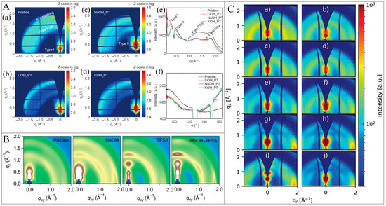
Figure 20.
(A). (a–d) GIWAXS pictures, (e) profiles for full integration lines, and (f) peak intensity at a q value of ca. 1.83 Å−1 (for PEDOT π−π stacking) with respect to the azimuthal angle (φ) for various alkali-treated DMSO/PEDOT:PSS films. The dip domains in the signal intensity profile in (e,f) correlated with the Pilatus detector gaps. qr is the parallel component of the scattering vector; qz is the scattering vector along the near-out-of-plane direction; and q is the scattering vector. Adapted with permission from ref. [278] Copyright 2021, Elsevier. (B). GIWAXS pictures of untreated PEDOT:PSS films and those doped by MeOH and TFSA, as well as those subjected to MeOH-TFSA dual treatments. Adapted with permission from ref. [304] Copyright 2025, Wiley. (C). 2D GIWAXS results/patterns for PEDOT:PSS specimens: (i,j) H2SO4, (g,h) HNO3, (e,f) HCOOH, (c,d) HCl, (b) EG treatment, and (a) untreated and their H2O-rinsed/washed counterparts. Adapted with permission from ref. [300] Copyright 2019, Wiley.
As shown in Figure 20B, Park et al. also explored the distinctive effects of PEDOT:PSS film treatment by trifluoromethanesulfonic acid (TFSA) on intra-grain transport by examining GIWAXS results/patterns. In contrast to untreated PEDOT:PSS films, which have an amorphous structure, the MeOH and TFSA treatments caused the appearance of multiple strong diffraction peaks [304].
In another work, 2D GIWAXS information/data were further depicted for (i) sulfuric acid (H2SO4), (g) nitric acid (HNO3), (e) formic acid (HCOOH), (c) hydrochloric acid (HCl), (b) ethylene glycol (EG)-treated films, and (a) untreated PEDOT:PSS film, as portrayed in Figure 20(Ca–Ci); the obtained Figure 20(Cd,Cf,Ch,Cj) reveals additionally H2SO4-, HNO3-, HCOOH-, and HCl-treated films which were subjected to H2O rinsing. The spots creating the results/patterns in 2D space clearly display distinguishable Bragg peaks in the qz direction—originating from lamellar stacking of the alternating PEDOT chain and PSS chain—that were usually observed in both GIWAXS and XRD observations in PEDOT:PSS films [300,305,306]. The H2SO4-treated sample in Figure 20(Ci) exhibited the most particular Bragg peak positions in the qz direction, which were attributed to a much higher order and were accompanied by the highest σ values among the studied treatment approaches. This can support the link between well-improved order in the crystalline structure and higher σ. Nevertheless, this higher order appears to be destroyed by following H2O rinsing/washing. Moreover, as shown in Figure 20(Ca) for the pristine specimen, a higher-intensity non-oriented signal was observed at about q ≈ 1.3 Å−1, which can be ascribed to a π-π stacking distance of ca. 4.8 Å between PSS in the amorphous PSS chains [305]. Remarkably, the signal for amorphous PSS was diminished for the various treatments, showing the depilation of the rich PSS chains in the thin films. The slightest signal in amorphous PSS chains was observed for the H2SO4- and HNO3-treated specimens, which went together with the significant thickness reduction induced by these treatments (Figure 20(Ca)). Below the diminished amorphous chains of PSS signal, additional oriented Bragg peaks were observed, particularly for H2SO4- and HNO3-treated films (Figure 20(Cg,Ci). Particular Bragg peaks at about 1.25 Å−1 and 60° were observed, perhaps created from an oriented chain of PSS π−π stacking, which was created by a templating impact of crystallizing and neighboring PEDOT. Together with the depilated content of the PSS chain, an extra oriented Bragg peak at about a q value of 40° and 1.75 Å−1 was discovered—this might be assigned to an extra orientation in π−π stacking of PEDOT within the edge-on and face-on orientation. For all that, the above-mentioned scattering patterns/results were a further explanation for higher crystallinity. The change/shift in the orientation of stacking distance within edge-on and face-on was observed earlier; however, it is often enclosed with the signal originating from the profile of highly non-oriented π−π stacking of PEDOT. Nevertheless, in this situation, the peak was visibly detached from the π−π stacking of PEDOT between edge-on and face-on [300].
3.5.2. XRD
XRD approaches are powerful and non-destructive characterization instruments with minimal specimen preparation. XRD analysis can be applied to scrutinize both crystalline materials (i.e., materials having long-range order of atomic arrangement) and noncrystalline materials (i.e., materials revealing a short order of atomic arrangement). XRD offers the first information in terms of crystal defects, degree of crystallinity, texture coefficient, orientation parameter, micro and macro strain, average crystallite size, crystalline structure, phase of materials, and electron density. When radiation impinges on a solid, scattering of the coherent radiation through periodically spaced samples of atoms yields scattered beams that create both spot features from a single crystalline specimen and ring patterns from a polycrystalline specimen. The patterns/results and intensities of the diffraction maxima (lines or peaks), as well as their position (interplanar spacing dhkl or Bragg angle θ), can be correlated to a specific crystal structure. XRD characterization gives information about the bulk and polycrystalline thin films, as well as multilayer structures, which is vital in various scientific and material science/engineering disciplines [307,308,309]. While infrared spectroscopy (IR), mass spectrometry (MS), and nuclear magnetic resonance (NMR) are better suited for gases and liquids (and solids in relation to NMR), XRD can elucidate the crystal structure [307].
For instance, Figure 21A displays the XRD results of the PEDOT:PSS thin films treated by different concentrations of H2SO4. For the untreated PEDOT:PSS (i.e., for pristine without any treatment by H2SO4), the XRD results possessed four typical peaks—25.6° (d = 3.5 Å), 17.7° (d = 5.0 Å), 6.6° (d = 13.4 Å), and 2θ = 3.8° (d = 23 Å)—in which the lattice spacing (d) was determined by employing Bragg’s law. The high-angle reflections at 2θ = 25.6° and 17.7° were attributed to inter-chain interaction stacking structure distance (010) of PEDOT and the amorphous halo of PSS, respectively, while the two lower 2θ peaks at 6.6° and 3.8° were indexed to a lamellar stacked distance (100) for the two distinct alternate orderings of PSS and PEDOT. XRD results showed that the PEDOT:PSS films slowly changed with the increase in the concentration of H2SO4. Following 20% and 50% H2SO4 treatment, the 2θ peaks at 6.6° and 3.8° were shifted to a lower angle by approximately 0.4° with an increase in intensity in the XRD information, which shows enhanced crystallinity and a raised lamella stacking distance. Nevertheless, in accordance with the σdc tests, notable alterations were seen following treatment with 80% H2SO4, in which PEDOT:PSS displayed two stronger d(100) 2θ peaks at 6.2° and 4.4°, with second-order d(200) 2θ peaks at 13.3°and 9.2°. On the other hand, the PEDOT:PSS treated by the 100% H2SO4 sample displayed only a stronger 2θ peak at 6.2°, with a second-order reflection peak at ca. 13.3°. The observations showed that the PEDOT:PSS film preferred a specific type of lamellar stacking for the two separate alternating orderings of PSS and PEDOT with the increase in H2SO4 concentrations [67].
In addition, pristine, DMSO-treated, and TFMS−MeOH-treated PEDOT:PSS thin films were examined by XRD to elucidate the mechanism of the enhanced TE performance, as portrayed in Figure 21B [282]. The two peaks at 2θ = 25.6° and 3.5° in the untreated PEDOT:PSS film were assigned to the lattice d spacings of 3.5 Å and 25.2 Å, as estimated using 2d sin θ = λ (Bragg’s law). The d spacing of 25.2 Å, which was discovered at 2θ ≈ 3.5°, was ascribed to the lamellar stacking distance (100) because of the distinct alternate ordering distance in the PEDOT chain and PSS. This lamella stacking distance was in good agreement with the widths of the PEDOT chain and PSS chain, which were 7.5 Å and 15.5 Å, respectively, as calculated based on chemical structural simulation [310]. In contrast, the d spacing at ∼3.5 Å detected at about 2θ = 25.6° was ascribed to the π−π stacking distance (010) in the PEDOT. Following treatment with TFMS−MeOH, there was negligible alteration within the lamella stacking distance, ranging from 25.2 Å to 23.2 Å, whereas the π−π stacking distance gradually decreased within the range of 3.5 to 3.4 Å. The decreases in π−π stacking distance imply that both the PEDOT chain and PSS chain were changed from the benzoid configuration to the quinoid configuration and hence attained a more planar structure following treatment by TFMS−MeOH. Moreover, the peak linked with the distance (010) plane was reduced compared with that of the distance (100) plane following treatment with TFMS-MeOH, implying this treatment resulted in a shift in the PEDOT:PSS layer orientation along the perpendicular direction to the substrate. In contrast with untreated PEDOT:PSS XRD peaks, the TFMS−MeOH-treated thin film resulted in shaper diffraction characteristic peaks with a higher intensity within the lower-angle reflections at 2θ = 3.8° and 6.6°, assigning distinctly to the lamella stacking distance (100) of two separate alternate orderings for the PEDOT chain and PSS chain, indicating a high degree of crystallization in PEDOT:PSS thin films [282].
Furthermore, XRD analysis was used to inspect the crystallinity of the PEDOT:PSS thin films treated by a combination of HNO3 and 1−butyl−3−methylimidazolium trifluoromethanesulfonate ([bmim][OTf]), or 1−butyl−3−methylimidazolium tetrafluoroborate ([bmim][BF4]), as depicted in Figure 21C. The HNO3-treated PEDOT:PSS (denoted as N−PEDOT:PSS) film exhibited a huge transformation in the intensity spectra of d(100), along with a noticeable existence of the second-order diffraction peak of d(100) at about 2θ = 13.0°, whereas a negligible transformation within the distance of lamella stacking for the two separate alternative alignments of the PEDOT and PSS was discovered from 13.0 to 13.4 Å, and the distance of π−π stacking was also slightly raised from 3.4 Å to 3.5 Å. The increase in π-π stacking distance upon HNO3 treatment showed the conversion of PEDOT from a benzoid structure into a quinoid structure, leading to the creation of a more planar configuration. In addition, the diffraction peak distance (100) intensity was considerably elevated following HNO3 treatment. Compared with N-PEDOT:PSS, the diffractions of distance (100) at the lower angle for both ([bmim][OTf])-treated N−PEDOT:PSS and ([bmim][BF4])-treated N−PEDOT:PSS films were somewhat shifted to about 6.6°, assigning to the lattice a d spacing of ca. 13.2 Å, and a slight decrease in intensity of the diffraction signal was discovered, creating a decrease in crystallinity that is possibly pertinent to the reduction in σ following post-treatment by ILs. The distance of diffraction peak intensity (100) was notably enlarged, which was ascribed to the rise in thin-film crystallinity and an increase in several ordered aggregates within the interchain synergic π−π stacking in the PEDOT chains. Additionally, the inclusion of IL preferentially elevated the π−π coupling within PEDOT:PSS, boosting the crystallinity and charge carrier mobility. Hence, the PEDOT:PSS thin films treated by the combination of HNO3, [bmim][OTf], and [bmim][BF4] resulted in an enhanced PEDOT:PSS interchain coupling and densely packed PEDOT chains with lamella stacking within the two kinds of assemblies, resulting in elevated S of the PEDOT:PSS thin films by interface scattering. Importantly, interface scattering comprises grain boundary scattering and surface scattering. The interface scattering mechanism in the charge carrier transport of PEDOT:PSS thin films has an essential function in both the σ and S of PEDOT:PSS films. The post-treatment removed PSS along with the increase in crystallinity of PEDOT, resulting in transformations of the grain size and grain boundaries of PEDOT, therefore improving TE performance [311].
In another study, the XRD was employed to understand the mechanism of TE behavior improvement in PEDOT:PSS thin films treated with CH3NO, CH3NO−H2SO4, and CH3NO−H2SO4−NaBH4, as shown in Figure 21D. In addition to the depilation of excess/rich PSS chains, another cause for the largely elevated diffraction peak intensities was the change in the molecular configuration of PEDOT chains from a benzoid configuration to a quinoid structure, caused by the post-treatment with H2SO4. In the average molecular configuration change, a C−C single bond within two different monomers was substituted through a π bond. The quinoid behavior prefers the PEDOT chain extension, resulting in an improved crystallized molecular configuration. In CH3NO−H2SO4−NaBH4-treated PEDOT:PSS, the treatment by NaBH4 solution (a strong reducing agent) was aimed to boost the S and σ of the PEDOT:PSS specimen by modulating its level of oxidation. This reduction process was reversed into the oxidation process by H2SO4e post-treatment, causing a molecular configuration reversion from quinoid behavior to benzoid behavior. In this XRD result, reductions in the intensities of the first diffraction peak positions of the two doublet peaks and a minor shift/move to higher 2θ values were observed, originating from this reversed change/transformation. With the removal of quinoid behavior, more compact and coiled conformations of PEDOT chains were detected [290].

Figure 21.
(A). XRD results for H2SO4-treated PEDOT:PSS thin films. Adapted with permission from ref. [67] Copyright 2014, Wiley. (B). XRD results of pristine PEDOT:PSS thin films with various solvent treatments. Adapted with permission from ref. [282] Copyright 2018, The Royal Society of Chemistry. (C). XRD results for (d) [bmim][BF4] −N−PEDOT:PSS; (c) [bmim][OTf] −N−PEDOT:PSS; (b) N−PEDOT:PSS; and (a) pristine films. Adapted with permission from ref. [311] Copyright 2020, The Royal Society of Chemistry. (D) XRD patterns for PEDOT:PSS thin films with various chemicals under different conditions. Adapted with permission from ref. [290] Copyright 2019, American Chemical Society.

Table 1.
Summary of spectroscopic and microscopic techniques applied for characterization of TE properties of some typical PEDOT:PSS polymers reported in recent years.
Table 1.
Summary of spectroscopic and microscopic techniques applied for characterization of TE properties of some typical PEDOT:PSS polymers reported in recent years.
| PEDOT:PSS-Based TE Materials Through Various Post-Treatments | Characterization | Achievements | PF (μW/mK2) | σ (S/cm) | S (μV/K) | Ref. |
|---|---|---|---|---|---|---|
| Pristine (untreated) PEDOT:PSS | XPS, UPS, RS, AFM, XPS, CVs, RS, UV−Vis−NIR, and XRD | The k and ZT of pristine PEDOT:PSS were measured to be <1 W/mK and in the order of 10−6, respectively | <0.04 | <1 | 15–18 | [69,70,83,282,312,313,314,315,316] |
| Triflic acid | RS and UV-Vis-NIR | TE properties were enhanced by both σ and S simultaneously | 94 | 1686 | 23.6 | [317] |
| Tetrahedrite (TH) Cu12+xSb4S13 | SEM, RS, and AFM | The greatest TE performance/properties were attained for a pellet specimen with a ZT value of ca. 0.12 at 473 K | 0.19 | 80 | 120 | [318] |
| Cu0.98Zn0.02FeS2/PEDOT:PSS | SEM, XRD, RS, and EDX | Nontoxic, inexpensive, and abundant Zn-doped chalcopyrite (Cu1−xZnxFeS2 with x = 0.03, 0.02, and 0.01) was combined with PEDOT:PSS | 19.1 | 18.2 | −61.3 | [319] |
| Cu0.98Zn0.02FeS2/PEDOT:PSS/graphene | SEM, XRD, RS, and EDX | The optimum film preserved above 80% of the σ after bending cycles of 2000, and a five-leg TE prototype built for optimum ternary films produced 4.8 mV at ΔT = 13 °C. | ∼23.7 | 77.4 | −61.3 | [319] |
| DMSO/PEDOT:PSS/SWCNTs/NaBH4 | AFM, SEM, XPS, RS, | A home-made TE device, manufactured employing eight pieces of PEDOT:PSS/SWCNTs films, exhibited a power output of 391 nW for ΔT = 20 K | 411 | 1718 | 49 | [320] |
| HNO3/passing N2 gas | XPS, UV−Vis−NIR, AFM, CVs, XRD, and RS | The HNO3 treatment was responsible for the loss of insulating excess PSS while the N2 gas pressure was responsible for the PEDOT chain conformational change | 94.3 | 2693 | - | [312] |
| Polyaniline, polypyrrole, and polythiophene | AFM, FE−SEM, FR−IR, UV−Vis, TEM, and XPS | The organic composite polymers offer high flexibility, PF, and efficient TE devices | 512 | 744 | 83 | [321] |
| Formic acid | SEM, AFM, XPS, and UV−Vis | Formic acid—possessing a higher dielectric constant—screened the charge between the PEDOT chain and PSS chain, leading to phase separation between them | - | 2050 | - | [289] |
| Formamide/SFS | AFM, UV−Vis−NIR, RS, XPS, and XRD | The cross-plane k of the untreated/pristine film was decreased from 0.59 W/mK for the untreated/pristine film to 0.29 W/mK for the SFS-F-PEDOT:PSS film, resulting in a ZT value that ranges from ca. 0.07 to ca. 0.14 at 300 K | 185.8 | 693 | 51.8 | [316] |
| H2SO4, NaOH(DMSO)/(N−DMBI) | AFM, UV−Vis, RS, XPS, and UPS | The highest PF for solid polymer films was established | 765.1 | 1864 | 64.1 | [43] |
| Femtosecond laser irradiation | UV−Vis−NIR, RS, XRD, and TGA | A simple, environmentally friendly strategy without any chemical dopants and treatments was established | 19 | 803.1 | - | [322] |
| Femtosecond laser/ammonia vapor atmosphere | UV−Vis−NIR, RS, XRD, and TGA | The prepared organic TE device shows an output voltage of 5.3 mV at a ΔT = 40.6 °C | 28.24 | 413.19 | 26.15 | [323] |
| Femtosecond laser irradiation/EMIM-DCA (IL) | UV−Vis−NIR, RS, XRD, and TGA | A TE device generated a voltage of 0.8 mV at ΔT = 11.7 K | 40.89 | 960.7 | 20.63 | [324] |
| EMIM:TCM | UV−Vis−NIR, RS, and XRS | The hybrid showed the best performance by optimizing both the σ and S | 175 | 1163 | 38.8 | [297] |
| Bi2Te3/rGO | XRD, RS, SEM, and XPS | A 12-fold increase was exhibited as compared to the original PEDOT films by greatly enhancing TE performance | 93.16 | 1522.4 | 24.7 | [325] |
| H2SO4/NaOH/Vitamin C/ EMIM:DCA | XPS, RS, AFM, FESEM-EDS, and UV−Vis−NIR | The greatest ZT value of 1.05 (world record) was recorded for polymer composites | 1285 | 1043 | 111 | [65] |
| H2SO4 and TDAE solution | UV−Vis−NIR, RS, XPS, and AFM | The water treatment before the TDAE solution treatment is crucial for the high | 526 | 1552 | 58.2 | [84] |
| Anthracene, naphthalene, and pyrene | UV−Vis, XPS, SEM, AFM, and UPS | TE properties that were enhanced by the splitting of the lower polaron energy level of PEDOT and inducing the π−π overlapping between the conjugated PEDOT and aromatic compounds | 289 | 1404 | 45.5 | [86] |
| MeOH | XPS and UPS | MeOH treatment partly restored the electrical behaviors of the denatured PEDOT:PSS films | 0.64 | 22.69 | 16.9 | [150] |
| PEGL with MeOH | 8.66 | 345.20 | 15.8 | |||
| Bi0.5Sb1.5Te3 | AFM, FE−SEM, XRD, SAXS, WAXS, and UV−Vis−NIR | 40 wt.% BST particles with a mean size of 1.389 mm at room temperature | 50 | 1050 | 215 | [326] |
| Acid (H2SO4)/base (NaOH)/ (DMSO)/DMSO solution of TTF | AFM, XPS, RS, and UV−Vis−NIR | Greatly enhanced the S but did not affect σ too much, thus resulting in a huge improvement in the overall TE properties and obtained a ZT value of 0.80 ± 0.04 | 1285 ± 67 | 2554 ± 161 | 71.0 ± 4.1 | [77] |
| MeOH | FTIR, XPS, SEM, UV-Vis, XPS, and AFM | Enhanced σ by four orders of magnitude | - | 1362 | - | [277] |
| Formic acid | XPS, RS, and AFM | ZT of ca. 0.32 was recorded by employing the Harman technique at room temperature | 80.6 | 1900 | 20.6 | [327] |
| H2SO4, water, and ethanol solution of TDAE | AFM | Outstanding TE behaviors/properties by the sequential treatments | 526 | 1552 | 58.2 | [84] |
| DMSO | AFM, UV−Vis, RS, and XPS | DMSO post-treatment resulted in a boosted σ and S. | 30.1 | 930.41 | 17.99 | [264] |
| Formamide | XPS, AFM, RS, and UV−Vis | The post-treatment decreased the cross-plane k from ca. 0.54 to ca. 0.19 W/mK, resulting in a ZT = 0.04 at room temperature | 88.7 | ≈2929 | 17.4 | [70] |
| HNO3/imidazolium-based ILs | AFM, UV−Vis, RS, XPS, and XRD | The κ correspondingly reduced from 0.6 to 0.3 W/mK for the pristine and treated PEDOT:PSS films. ZT = ca. 0.12 was attained at 300 K. | 11.2 | 1260 ± 61 | 34.8 ± 1.8 | [311] |
| Formic acid/HZ | AFM, UV−Vis, RS, and XPS | The substantial improvement in the S and the PF was ascribed to the depilation of the PSS chain—and more essentially—the decrease in the PEDOT doping level by HZ treatment | 93.5 | 514 | 42.7 | [69] |
| DMSO/EMIMBF4 | AFM, UV−Vis, RS, and XPS | The corresponding ZT was obtained to be 0.068 by assuming a k = 0.17 Wm/K at 300 K | 38.46 | - | - | [264] |
| Formamide/SFS/imidazolium-based ILs | AFM, UV−Vis, RS, XPS, UPS, and XRD | An optimized PF of ~239.2 μW/K2m was obtained after sequential post-treatment | ~239.2 | 641 | 61.1 | [263] |
| CH3NO)/H2SO4/NaBH4 | AFM, UV−Vis, XPS, SEM, and XRD | The TE device resulted in a higher output power density = ca. 1 μW/cm2 using the human arm as a heating source | 141 | 1786 | 28.1 | [290] |
| TFA | AFM, UV−Vis, RS, and XPS | More importantly, ~80% of the S and σ was retained after 20 days | 97.1 ± 5.4 | 3748 | 16.0 ± 1.1 | [313] |
| DMSO/H2SO4 | AFM, RS, SEM, and XPS | The TE device exhibited an output power = 2.25 nW using a ΔT of 25 K | 80.8 | 4464 | - | [328] |
| TFMS−MeOH | AFM, UV−Vis, XPS, RS, and XRD | At the optimized conditions, the ZT value was found to be 0.19. | 142 | 2980 | 21.9 | [282] |
| Sulfuric acid/PSSH | In situ RS | The enhancement in the S by polyelectrolytes was ascribed to the EF resulting from the individual ion Soret effect | 401 | 2120 | 43.5 | [329] |
| Sulfuric acid/base/PSSNa | In situ RS | The EF resulting from the ion individual Soret effect by polyelectrolytes enhanced the S | 401 | 1732 | 48.1 | [329] |
| H2SO4 | XRD, HAADF−STEM, and UV−Vis−NIR | The concentrated H2SO4 post-treatment resulted in highly ordered crystalline PEDOT:PSS nanofibrils | - | 4380 | - | [67] |
| HNO3 | AFM, UV−Vis−NIR, XPS, RS, and XRD | HNO3 post-treatment significantly enhanced the σ value with a small drop in S | 76.0 ± 5.3 | 3200 ± 89 | 16 ± 1.2 | [311] |
| [bmim][OTf]/HNO3 | UV−Vis−NIR, AFM, XPS, RS, and XRD | The PEDOT:PSS films were stable, and more than 85% of their σ and S values were retained at 75% RH and 70 °C for 20 days | ∼152 ± 11.2 | 1260 ± 61 | 4.8 ± 1.8 | [311] |
| [bmim][BF4]/HNO3 | AFM, UV−Vis−NIR, XPS, RS, and XRD | Maintained excellent long-term stability at 75% RH and 70 °C for 20 days | 137 ± 12.5 | 1188 ± 45 | 33.9 ± 1.9 | [311] |
| PSVA using DMSO | FE-SEM, XPS, UPS, and GIWAXS | The PSVA treatment approach increased the EF impact of PEDOT:PSS/Bi2Te3 NWs | 226 | 1026 | 47 | [276] |
| DMSO/HZ | AFM, RS, XPS, and UV−Vis−NIR | An optimized PF was obtained for HZ (0.0175 wt.%) in DMSO-treated film at room temperature. | 112 | 2 | 142 | [66] |
| Alkali Base (KOH) | UV−Vis−NIR, AFM, GIWAXS, and ATR−FTIR | The post-treatment approaches employed were simple and green alkali–base solutions | 50.0 | 184 | 51.9 | [278] |
| MeOH/TFSA | AFM, GIWAXS, RS, and XPS | A secondary vapor treatment method was employed | 104.2 | 2053 | 22.5 | [304] |
| MSA | RS, XPS, and UV−Vis | This treatment approach induced secondary doping and significantly improved σ | 75 | 2998 | 15.8 | [56] |
| Acid (MSA)/Base (NaOH) | RS, XPS, and UV−Vis | The enhancement in S and PF can be ascribed to the partial dedoping of the PEDOT chain by NaOH | 258 | 1835 | 37.5 | [56] |
| Acid/base/R101 | SEM, EDX, FS, RS, XPS, UV−Vis, and UPS | The k of pristine and PRAB were measured to be 0.204 and 0.234 W/mK, respectively, as recorded by the laser flash method. Hence, the optimal ZT = 0.46 achieved for PRAB. R101 (with a conjugated structure) provided the highest increase in S. The boost of S was ascribed to EF caused by the zwitterion dipole moment and the π−π overlapping between PEDOT:PSS and conjugated R101. | 546 | - | 61.6 | [56] |
| Acid/base/DMCSP | RS, XPS, FS, UV−Vis, and UPS | DMSCP (with a conjugated pyridine ring) offered modest S | 385 | - | 55.5 | [56] |
| Acid/base/DDMAP | RS, XPS, UV−Vis, and UPS | DDMAP (with a saturated structure) offered the slightest improvement in S | 323 | - | 46.8 | [56] |
| Ti3C2Tx | XRD, SEM, UPS, XPS, and UV−Vis | Enhanced S for a p-type polymer/n-type filler TE composite has been discovered for the first time. The enhancement in S was ascribed to the EF effect. | 140.1 | 736.4 | 43.6 | [275] |
| H2SO4 | UV−Vis, RS, and AFM | Detailed Raman map analysis clarified microstructural behaviors distributed in large areas caused by dopants | - | 4358 | - | [330] |
Abbreviations: Thermoelectric properties: Electrical conductivity (σ); power factor (PF); thermal conductivity (k); Seebeck coefficient (S); and figure of merit (ZT). Various treatment materials: 1-ethyl-3-methylimidazolium dicyanamide (EMIM:DCA); polydimethylsiloxane (PDMS); 1-ethyl-3methylimidazolium: tricyanomethanide (EMIM:TCM); reduced graphene oxide (rGO); 1-ethyl-3-methylimidazolium tetrafluoroborate ([bmim][BF4]); lithium tetrafluoroborate (LiBF4); 1-butyl-3-methylimidazolium trifluoromethanesulfonate- [bmim][OTf]; sodium formaldehyde sulfoxylate (SFS); 1-Ethyl-3-MethylImidazolium DiCyAmide (EMIM-DCA); 5 wt.% glycerol loaded into the PEDOT:PSS solution (PEGL); 1-ethyl-3-methylimidazolium tetrafluoroborate (EMIMBF4); Vf = volume fractions; 1-butyl-3-methylimidazolium tetrafluoroborate (BMIM-BF4); rhodamine 101 (R101); 1-butyl-3-methylimidazolium bis(trifluoromethanesulfonyl) amide (BMIM-TFSI); N-dodecyl-N,N-dimethyl-3-ammonio-1-propane-sulfonate (DDMAP); tetrahedrite (TH) (Cu12+xSb4S13); 1-(N,N-dimethylcarbamoyl)-4-(2-sulfoethyl) pyridinium hydroxide (DMCSP); NanoMap-PS (NM-PS); Poly(3,4-ethylenedioxythiophene):poly(styrene sulfonate) (PEDOT:PSS); nitric acid (HNO3); nitrogen (N2); sulfuric acid (H2SO4); dimethyl sulfoxide (DMSO); sodium hydroxide (NaOH); bismuth telluride (Bi2Te3), tetrakis(dimethylamino)ethylene (TDAE); methanol (MeOH); tetrathiafulvalene (TTF); hydrazine (HZ); 1-ethyl-3-methylimidazolium tetrafluoroborate (EMIMBF4); sodium formaldehyde sulfoxylate (SFS); formamide (CH3NO); sodium borohydride (NaBH4); trifluoroacetic acid (TFA); trifluoromethanesulfonic acid (TFMS); Poly(4-styrenesulfonic acid) (PSSH); 4-(1,3-dimethyl-2,3-dihydro-1H-benzoimidazol-2-yl)phenyl)dimethylamine (N-DMBI); poly(sodium 4-styrenesulfonate) (PSSNa); nitric acid (HNO3); polar solvent vapor annealing (PSVA); potassium hydroxide (KOH); trifluoromethanesulfonic acid (TFSA); methanesulfonic acid (MSA); MXene (Ti3C2Tx); bismuth antimony telluride alloy (Bi0.5Sb1.5Te3); Single-walled carbon nanotubes (SWCNTs); Zn-doped chalcopyrite (Cu1−xZnxFeS2), and 4-(1,3-dimethyl-2,3-dihydro-1H-benzoimidazol-2-yl)phenyl)dimethylamine (N-DMBI). Characterization techniques: Attenuated total reflectance Fourier-transform infrared spectroscopy (ATR-FTIR); cyclic voltammograms (CVs); ultraviolet–visible–near-infrared (UV-Vis-NIR) spectroscopy; small-angle X-ray scattering (SAXS); Raman spectroscopy (RS); fluorescence spectroscopy (FS); ultraviolet photoelectron spectroscopy (UPS); scanning electron microscopy (SEM); atomic force microscopy AFM; field emission scanning electron microscopy (FE-SEM); X-ray photoelectron spectra (XPS); thermogravimetric analysis (TGA); grazing incidence wide-angle X-ray scattering (GIWAXS); and high-angle annular dark-field scanning transmission electron microscopy (HAADF-STEM).
Table 2.
Comparison of various modern characterization approaches in terms of sample preparation, main information, advantages, and limitations for analysis of materials.
Table 2.
Comparison of various modern characterization approaches in terms of sample preparation, main information, advantages, and limitations for analysis of materials.
| Techniques | Sample Preparation | Main Information | Advantages | Limitations | Ref. |
|---|---|---|---|---|---|
| SEM |
| Surface topography, size, and elemental composition of specimens using EDS or WDS, surface morphology, structure/shape, and crystallography of materials |
|
| [117,331,332,333,334,335,336,337,338,339] |
| FE-SEM |
| Surface morphology, elemental composition of the specimen by employing EDS or WDS, sample surface, size, and geometry |
|
| [336,340] |
| SEM-EDS | Has an energy of ca. 40 keV Can be used for various samples | Chemical composition, external morphological, elemental analysis, and dispersion, nanostructure |
|
| [338,339,341,342] |
| EDS | The samples prepared for SEM can be analyzed/detected directly by EDS. Nevertheless, if there is specimen coating owing to poor conductivity, the coating material which can be detected/analyzed in the EDS spectra requires a careful selection of coating material so that it cannot overlap with the elements present in the specimen | Chemical formula and elemental/chemical composition of the sample |
|
| [117,343,344] |
| AFM |
| Morphology, distribution, surface roughness, surface structure, mechanical and electrical properties, size (10−20 nm lateral resolution, <1 vertical resolution), and 3−D shaping |
|
| [117,331,332,333,334,335,336,337,342,345,346,347] |
| TEM |
| Microstructure, shape, NP size, aggregation state, topology, elemental, crystal structure, conductivity or magnetics, growth kinetics of composites, defects in the specimen, and detect and quantify NPs in matrices |
|
| [117,332,333,335,336,342,346] |
| XPS |
| Chemical states, elemental composition, oxidation states, specimen surface, electronic structure, crystallographic, surface, degradation, and functional group |
|
| [117,118,331,332,334,341,342,345,346,348,349] |
| XRD |
| Crystal structure, structure, orientation, size, phase, composition, crystalline size (1 nm to 100 nm), crystallographic, nature of the phase, elemental composition, sample purity, crystalline grain size, lattice parameters, and the chemical compounds |
|
| [117,331,334,335,337,341,342,346] |
| GIWAXS | Thin films No extensive specimen preparation | Crystal information at steady state, and composition evolution | It can be employed for the investigation of functional thin films, in situ observation, depth resolution, rich structural information, non-destructive and no-contact probing, sensitive structural resolution, and high signal-to-noise ratio | Influenced by energy range, size, flux, and 2D area detector behaviors focusing on optics, the incident X-ray beam shape, and the spatial and temporal resolution of the detector | [292,293,301,350,351,352,353] |
| UPS | Surfaces and thin-film specimens are required to be vacuum-compatible, and specimens are required to be free from surface adsorbates, oxides, or contaminants Specimen preparation approaches such as handling, drying, and cleaning may alter the surface properties or introduce artifacts. Requires a specimen that can efficiently emit lower-energy electrons that limit the conductive or semi-conductive materials for their purposes | Electronic structure/properties, band structure, and energy levels | Non-destructive and provides interface and surface behaviors with atomic-scale resolution Investigates molecule electronic structures, atoms, and solids. Estimates the Φ of a material. Gives insights into interface phenomena, surface reactions, electronic behaviors of semi-conductor devices, and energy levels of inorganic and organic materials |
| [118,354,355] |
| UV−Vis | Non-destructive measuring method for inorganic, organic, and biological material | Enable monitoring chemical reactions in real time by estimating transformations in absorbance/transmission with respect to time, hints on the shape of the NP, molecular structure, electronic transitions, size (structural properties), aggregation conditions, concentration, elemental composition, functional group, optical properties, and bandgap energy information |
|
| [118,331,337,341,342,356,357] |
| RS | Minimal specimen preparation Specimen preparation stages such as mounting, grinding, and drying can bring artifacts or change specimen behaviors, possibly influencing Raman spectra The Raman spectrometer specimen area is often <10 cm2 with a thickness <2.5 cm, put over a silicon or glass substrate | Chemical composition, bonding, molecular structure, functional groups, chain orientation properties of the material, and interfacial surface behaviors. It can detect diatomic molecules like nitrogen and oxygen. Non-destructive test and a comparatively simple method. | Excellent for studying transformations in the crystal structure of polymer owing to variations in the mechanical and chemical behaviors Offers information about composition, structure, and properties Highly functional group sensitivity with better peak intensity Can be employed for oxidation observations throughout a broad temperature range | Polar molecules possess smaller Raman signal Limited depth penetration, specimen heating, and requires a longer time for the analysis Fluorescent light release for certain specimens may result in background noise Raman spectra can be challenging and complex to interpret, particularly for specimens with mixtures of compounds, multiphase materials, or overlapping peaks | [117,118,334,349] |
| NMR | Careful specimen preparation, non-destructive. Requires a larger quantity of specimens, usually in the range of mg to µg. The specimen preparation needs skilled hands and requires maintaining the specimen’s solubility, stability, and purity | It offers dynamics of organic molecules at the atomic level. It gives comprehensive information on the structure, composition, molecular conformation, degradation, and functional group purity |
|
| [117,118,334,337,342,346,347,348,349,350,351,352,353,354,355,356,357,358] |
| TGA | A small quantity of specimen (usually 2 mg - 20 mg) is placed into a crucible (pan) of appropriate size, which is often built of materials like platinum or aluminum After that, the specimen is loaded into the TGA instrument | Thermal stability, composition and mass of stabilizers, and material decomposition kinetics |
|
| [118,334,341,342,346,359] |
| FTIR |
| Provides information for functional groups for liquid, solid, or gas specimens, surface composition, molecular structures and chemical compositions, molecular bonds between matter, compounds, molecules, compatibility, miscibility, and degradation and interaction of NPs |
|
| [117,118,283,341,342,360] |
| EELS | Thin films (<100 nm), conductive Thicker specimens may need thinning methods like focused ion beam milling or ion milling to decrease the effects of scattering | Electronic excitation, chemical bonding and functionality, collective atoms interaction with neighbors, elemental composition, atoms chemical state, collective interactions of atoms with their neighbors, the resonance of bulk plasma, and the number and type of atoms |
|
| [118,342,346,361,362,363,364,365] |
Abbreviations: scanning electron microscopy (SEM); Fourier-transform infrared spectroscopy (FT−IR); field emission scanning electron microscopy (FE−SEM); energy-dispersive X-ray spectroscopy (EDS); nuclear magnetic resonance (NMR); wavelength-dispersive X-ray spectroscopy (WDS); atomic force microscope (AFM); transmission electron microscopy (TEM); scanning electron microscopy–energy-dispersive X-ray spectrometry (SEM−EDS); X-ray photoelectron spectroscopy (XPS); electron; grazing incidence wide-angle X-ray scattering (GIWAXS); ultraviolet photoemission spectroscopy (UPS); Raman spectroscopy (RS); thermogravimetric analysis (TGA); X-ray diffraction (XRD); and energy loss spectroscopy (EELS).
4. Conclusions, Challenges and Future Perspective
4.1. Conclusions
In summary, in this review, we summarize both established and emerging spectroscopic and microscopic techniques that had already been applied for the characterization of inorganic and polymer TE materials, specifically PEDOT:PSS, with examples and how these modern approaches/techniques contribute to understanding the mechanism of the fundamental TE behaviors of inorganic and polymer TE materials that have been already reported in the literature with respect to electronic, structural, morphology and chemical features. This review offers an overview of the spectroscopic characterization for studying the mechanisms of TE enhancement in both inorganic and polymer TE materials, highlighting the recent developments in the field.
This review summarizes various spectroscopy and microscopy techniques that have already been applied for the characterization of inorganic and polymer TE materials. For inorganic TE, -EDX spectroscopy, UV−Vis spectroscopy, and XPS were widely applied for electronic structure characterization. For phase analysis of inorganic TE materials, RS, NMR spectroscopy, and EELS were utilized. For analyzing the surface morphology and crystalline structure, SEM, TEM, and XRD were commonly used. For polymer TE materials, UV−Vis−NIR spectroscopy and UPS were generally employed for determining electronic structure. For functional groups analysis of polymer TE, ATR-FTIR and RS were broadly utilized. XPS was used for elemental composition analysis of polymer TE. For the surface morphology of polymer TE, AFM and SEM were applied. GIWAXS and XRD were employed for analyzing the crystalline structure of polymer TE materials. In this paper, each spectroscopic technique is discussed by providing examples of spectroscopic techniques that have already been employed for TE characterization.
Overall, this review provided insight into the various characterization approaches applied for both inorganic and organic TE that were performed using a static approach—and it will provide the merits of understanding the properties and arrangement of TE composites and predict the performance of TE materials as well as optimize the manufacturing processes by boosting their specific properties—including σ, S, κ, thermal stability, environmental stability, mechanical strength, super-flexibility, and film formation, as well as their combined features. In addition, a thorough characterization of electronic, structural, morphological, and chemical features was provided to design novel approaches and materials with the required behaviors for boosting the TE properties.
Furthermore, the review looks ahead, recommending substantial future research areas. These comprise in situ spectroscopy and microscopy methods for tracking the dynamic evolution of a TE sample/specimen, as well as combining machine learning-assisted analysis with multi-dimensional and ultra-fast spectroscopy and microscopy approaches in order to boost TE performance.
Contemplating its importance today, we believe the review has the potential to be an important resource for researchers providing information about advanced spectroscopic and microscopic characterization techniques to predict the performance of TE materials/composites as well as data interpretation guidelines for potential applications in various disciplines such as electronic devices, including memristors and neuromorphic devices, organic electrochemical transistors (OECTs), light-emitting diodes (LEDs), photodetectors, and a hole transport layer (HTL) for solar cells, as well as energy storage devices including batteries and supercapacitors.
4.2. Challenges and Future Perspective
Despite the notable improvement in the performances of TE materials, they are still limited to the laboratory, and they are far from practical applications. Thus far, the TE characterization experiments reported were performed using a static approach without causing/inducing composition and structural transformation in the sample. These static analyses can offer substantial information on TE performance since they permit correlating the fundamental TE properties/behaviors with the composition and structure of the entire investigated sample at higher resolution, reaching down to the atomic-scale features. For instance, by manufacturing materials with typical defects for microstructural engineering, it would be attainable to estimate the contribution of a particular grain boundary engineering on the S. Nevertheless, an in situ method typically refers to the potential of tracking the dynamic evolution of a sample within in situ spectroscopy and microscopy. Hence, continued efforts are suggested to focus on the following issues to boost TE performance:
- (1)
- Advanced synchrotron-based analytical tools, including scattering and spectroscopy, as well as imaging capabilities combined with in situ and operando applications, have to be performed, as these approaches can give fundamental insights to understand the behaviors of TE materials, such as geometric and electronic structures under realistic operating conditions.
- (2)
- Emerging techniques such as machine learning-assisted analysis have to be combined with multi-dimensional and ultra-fast spectroscopy, and microscopy approaches have to be implemented, as they are promising approaches to further advance our understanding of basic relationships in TE materials and accelerate the discovery of materials.
- (3)
- Fundamental electronic band structure characterization by UV-Vis-NIR and photoelectron spectroscopy, as well as sophisticated lattice dynamics analysis via RS, has to be performed, as these techniques can give a deeper understanding of structure–property relationships for TE materials.
- (4)
- The combination of multiple spectroscopic techniques must be established, as this enables multiscale characterization spanning atomic to mesoscale phenomena, revealing the complex interplay between electronic transport, phonon scattering, and nanostructural features.
- (5)
- The synergy between material synthesis, advanced spectroscopic characterization, and property optimization has to be harnessed, as this can drive innovations in TE materials science. As we move toward more sophisticated materials with hierarchical structures and coupled functionalities, the role of comprehensive spectroscopic analysis becomes increasingly critical for achieving breakthrough performance levels.
- (6)
- The correlation between crystalline microstructure engineering and TE performance/properties is still unclear, and the mechanism of crystallization from a molecular engineering point of view, as well as structure–property correlations at atomic, nanoscale, and mesoscale levels, has to be investigated for the development of higher-performance organic polymers including PEDOT:PSS and organic/inorganic composites.
- (7)
- New methods and new post-treatment procedures, along with the optimization of fabrication approaches, filler materials, and interfacial engineering, as well as the development of theoretical models, have to be pursued to attain superior TE properties/performance for PEDOT:PSS- and PEDOT:PSS-based TE composites.
- (8)
- The EF technique has to be applied to boost S while slightly reducing σ and elevating PF for higher-performance polymer TE materials, including PEDOT:PSS.
Author Contributions
T.A.Y.: Conceptualization, Writing—Original Draft, Methodology, Supervision, Reviewing, and Editing; T.A.W.: Investigation, Data Curation, Writing—Original draft, Reviewing, and Editing; Y.Z. and W.S.C.: Conceptualization, Methodology, Supervision, Reviewing, and Editing. M.K.T. and T.G.B.: Data Curation, Reviewing, and Editing. All authors have read and agreed to the published version of the manuscript.
Funding
This research received no external funding.
Data Availability Statement
No new data were created or analyzed in this study.
Conflicts of Interest
The authors declare no conflicts of interest.
References
- Deng, L.; Liu, Y.; Zhang, Y.; Wang, S.; Gao, P. Organic thermoelectric materials: Niche harvester of thermal energy. Adv. Funct. Mater. 2023, 33, 2210770. [Google Scholar]
- Shi, X.-L.; Zou, J.; Chen, Z.-G. Advanced thermoelectric design: From materials and structures to devices. Chem. Rev. 2020, 120, 7399–7515. [Google Scholar] [CrossRef] [PubMed]
- Zhou, Y.; Ding, T.; Xu, G.; Yang, S.; Qiu, C.-W.; He, J.; Ho, G.W. Sustainable heat harvesting via thermal nonlinearity. Nat. Rev. Phys. 2024, 6, 769–783. [Google Scholar] [CrossRef]
- Qin, Y.; Qin, B.; Wang, D.; Chang, C.; Zhao, L.-D. Solid-state cooling: Thermoelectrics. Energy Environ. Sci. 2022, 15, 4527–4541. [Google Scholar] [CrossRef]
- He, J.; Tritt, T.M. Advances in thermoelectric materials research: Looking back and moving forward. Science 2017, 357, eaak9997. [Google Scholar] [CrossRef]
- Snyder, G.J.; Toberer, E.S. Complex thermoelectric materials. Nat. Mater. 2008, 7, 105–114. [Google Scholar] [CrossRef]
- Alajlan, A.M.; Dang, S.; Gan, Q. Enhanced nighttime power generation and photovoltaic cooling in photovoltaic-thermoelectric hybrid systems. Energy Convers. Manag. 2024, 22, 100580. [Google Scholar]
- Afaneh, D.; Bahaidarah, H.; Lawal, D.U.; Antar, M.A. Novel integration of thermoelectric distiller with direct contact membrane distillation. Energy Convers. Manag. 2024, 22, 100575. [Google Scholar]
- Azadinia, M.; Davidson-Hall, T.; Chung, D.S.; Ghorbani, A.; Samaeifar, F.; Chen, J.; Chun, P.; Lyu, Q.; Cotella, G.; Aziz, H. Inverted solution-processed quantum dot light-emitting devices with wide band gap quantum dot interlayers. ACS Appl. Mater. Interfaces 2023, 15, 23631–23641. [Google Scholar] [CrossRef]
- Vafadar, M.F.; Zhao, S. Ultralow threshold surface emitting ultraviolet lasers with semiconductor nanowires. Sci. Rep. 2023, 13, 6633. [Google Scholar] [CrossRef]
- Masoumi, S.; O’Shaughnessy, S.; Pakdel, A. Organic-based flexible thermoelectric generators: From materials to devices. Nano Energy 2022, 92, 106774. [Google Scholar] [CrossRef]
- Jabri, M.; Masoumi, S.; Sajadirad, F.; West, R.P.; Pakdel, A. Thermoelectric energy conversion in buildings. Mater. Today Energy 2023, 32, 101257. [Google Scholar] [CrossRef]
- Kishore, R.A.; Nozariasbmarz, A.; Poudel, B.; Priya, S. High-performance thermoelectric generators for field deployments. ACS Appl. Mater. Interfaces 2020, 12, 10389–10401. [Google Scholar] [CrossRef] [PubMed]
- Shi, X.-L.; Wang, L.; Lyu, W.; Cao, T.; Chen, W.; Hu, B.; Chen, Z.-G. Advancing flexible thermoelectrics for integrated electronics. Chem. Soc. Rev. 2024, 53, 9254–9305. [Google Scholar] [CrossRef]
- Massetti, M.; Jiao, F.; Ferguson, A.J.; Zhao, D.; Wijeratne, K.; Würger, A.; Blackburn, J.L.; Crispin, X.; Fabiano, S. Unconventional thermoelectric materials for energy harvesting and sensing applications. Chem. Rev. 2021, 121, 12465–12547. [Google Scholar] [CrossRef] [PubMed]
- DiSalvo, F.J. Thermoelectric Cooling and Power Generation. Science 1999, 285, 703. [Google Scholar] [CrossRef]
- Wood, C. Materials for Thermoelectric Energy Conversion. Rep. Prog. Phys. 1988, 51, 459. [Google Scholar] [CrossRef]
- Nolas, G.S.; Poon, J.; Kanatzidis, M. Recent Developments in Bulk Thermoelectric Materials. MRS Bull. 2006, 31, 199. [Google Scholar] [CrossRef]
- Cao, J.; Tan, X.Y.; Dong, J.; Liu, H.; Zheng, Y.; Zhu, Q.; Xu, J.; Zhang, G.; Wu, J.; Suwardi, A. Thermoelectric device performance beyond average ZT: Holistic consideration of materials and design. Mater. Today Phys. 2023, 34, 101071. [Google Scholar] [CrossRef]
- Cao, T.; Shi, X.-L.; Chen, Z.-G. Advances in the design and assembly of flexible thermoelectric device. Prog. Mater. Sci. 2023, 131, 101003. [Google Scholar]
- Xiao, Y.; Zhao, L.-D. Seeking new, highly effective thermoelectrics. Science 2020, 367, 1196–1197. [Google Scholar] [CrossRef]
- Zheng, Y.; Slade, T.J.; Hu, L.; Tan, X.Y.; Luo, Y.; Luo, Z.-Z.; Xu, J.; Yan, Q.; Kanatzidis, M.G. Defect engineering in thermoelectric materials: What have we learned? Chem. Soc. Rev. 2021, 50, 9022–9054. [Google Scholar] [CrossRef]
- Yu, Y.; Xu, X.; Bosman, M.; Nielsch, K.; He, J. Germanium-telluride-based thermoelectrics. Nat. Rev. Electr. Eng. 2024, 1, 109–123. [Google Scholar] [CrossRef]
- Suwardi, A.; Cao, J.; Zhao, Y.; Wu, J.; Chien, S.W.; Tan, X.Y.; Hu, L.; Wang, X.; Wang, W.; Li, D. Achieving high thermoelectric quality factor toward high figure of merit in GeTe. Mater. Today Phys. 2020, 14, 100239. [Google Scholar] [CrossRef]
- Suwardi, A.; Cao, J.; Hu, L.; Wei, F.; Wu, J.; Zhao, Y.; Lim, S.H.; Yang, L.; Tan, X.Y.; Chien, S.W. Tailoring the phase transition temperature to achieve high-performance cubic GeTe-based thermoelectrics. J. Mater. Chem. A 2020, 8, 18880–18890. [Google Scholar]
- Suwardi, A.; Lim, S.H.; Zheng, Y.; Wang, X.; Chien, S.W.; Tan, X.Y.; Zhu, Q.; Wong, L.M.N.; Cao, J.; Wang, W. Effective enhancement of thermoelectric and mechanical properties of germanium telluride via rhenium-doping. J. Mater. Chem. C 2020, 8, 16940–16948. [Google Scholar] [CrossRef]
- Jia, B.; Wu, D.; Xie, L.; Wang, W.; Yu, T.; Li, S.; Wang, Y.; Xu, Y.; Jiang, B.; Chen, Z. Pseudo-nanostructure and trapped-hole release induce high thermoelectric performance in PbTe. Science 2024, 384, 81–86. [Google Scholar] [PubMed]
- Bai, S.; Zhang, X.; Zhao, L.-D. Rethinking SnSe thermoelectrics from computational materials science. Acc. Chem. Res. 2023, 56, 3065–3075. [Google Scholar]
- Luo, Y.; Zheng, Y.; Luo, Z.; Hao, S.; Du, C.; Liang, Q.; Li, Z.; Khor, K.A.; Hippalgaonkar, K.; Xu, J. n-type SnSe2 oriented-nanoplate-based pellets for high thermoelectric performance. Adv. Energy Mater. 2018, 8, 1702167. [Google Scholar] [CrossRef]
- Zhang, Z.; Zhao, K.; Wei, T.-R.; Qiu, P.; Chen, L.; Shi, X. Cu 2 Se-Based liquid-like thermoelectric materials: Looking back and stepping forward. Energy Environ. Sci. 2020, 13, 3307–3329. [Google Scholar]
- Li, L.; Hu, B.; Liu, Q.; Shi, X.L.; Chen, Z.G. High-Performance AgSbTe2 Thermoelectrics: Advances, Challenges, and Perspectives. Adv. Mater. 2024, 36, 2409275. [Google Scholar] [CrossRef] [PubMed]
- Jiang, Y.; Su, B.; Yu, J.; Han, Z.; Hu, H.; Zhuang, H.-L.; Li, H.; Dong, J.; Li, J.-W.; Wang, C. Exceptional figure of merit achieved in boron-dispersed GeTe-based thermoelectric composites. Nat. Commun. 2024, 15, 5915. [Google Scholar] [CrossRef]
- Geng, Y.; He, H.; Liang, R.; Lai, Q.; Hu, L.; Liu, F.; Zhang, C. One-Step-Sintered GeTe-Bi2Te3 Segmented Thermoelectric Legs with Robust Interface-Connection Performance. Adv. Energy Mater. 2024, 14, 2402479. [Google Scholar]
- Shi, X.-L.; Li, N.-H.; Li, M.; Chen, Z.-G. Toward Efficient Thermoelectric Materials and Devices: Advances, Challenges, and Opportunities. Chem. Rev. 2025, 125, 7525–7724. [Google Scholar] [CrossRef]
- Li, N.; Wang, G.; Zhou, Z.; Wang, G.; Han, G.; Lu, X.; Zhou, X. IV-VI/I-V-VI2 Thermoelectrics: Recent Progress and Perspectives. Adv. Funct. Mater. 2024, 34, 2405158. [Google Scholar] [CrossRef]
- Pichanusakorn, P.; Bandaru, P. Nanostructured thermoelectrics. Mater. Sci. Eng. R Rep. 2010, 67, 19–63. [Google Scholar] [CrossRef]
- Zhang, Q.; Sun, Y.; Xu, W.; Zhu, D. Organic thermoelectric materials: Emerging green energy materials converting heat to electricity directly and efficiently. Adv. Mater. 2014, 26, 6829–6851. [Google Scholar] [CrossRef] [PubMed]
- Bahk, J.-H.; Fang, H.; Yazawa, K.; Shakouri, A. Flexible thermoelectric materials and device optimization for wearable energy harvesting. J. Mater. Chem. C 2015, 3, 10362–10374. [Google Scholar] [CrossRef]
- Zheng, Y.; Tan, X.Y.; Wan, X.; Cheng, X.; Liu, Z.; Yan, Q. Thermal stability and mechanical response of Bi2Te3-based materials for thermoelectric applications. ACS Appl. Energy Mater. 2019, 3, 2078–2089. [Google Scholar] [CrossRef]
- Zhu, B.; Su, X.; Shu, S.; Luo, Y.; Tan, X.Y.; Sun, J.; Sun, D.; Zhang, H.; Zhang, Q.; Suwardi, A. Cold-sintered Bi2Te3-based materials for engineering nanograined thermoelectrics. ACS Appl. Energy Mater. 2022, 5, 2002–2010. [Google Scholar] [CrossRef]
- Yemata, T.A. Enhanced Thermoelectric Properties and Environmental Stability of PEDOT: PSS Conducting Polymers by Various Chemical Post-Treatments. Ph.D. Thesis, National University of Singapore, Singapore, 2019. [Google Scholar]
- Yao, H.; Fan, Z.; Cheng, H.; Guan, X.; Wang, C.; Sun, K.; Ouyang, J. Recent development of thermoelectric polymers and composites. Macromol. Rapid Commun. 2018, 39, 1700727. [Google Scholar] [CrossRef]
- He, X.; Wu, C.; Zhang, T.; Chen, Z.; Wang, L.; Ouyang, J. Ultrahigh Thermoelectric Properties of PEDOT: PSS Films by Dedoping and π-π Overlapping With 4-(1, 3-dimethyl-2, 3-dihydro-1H-benzoimidazol-2-yl) phenyl) Dimethylamine (N-DMBI). Adv. Funct. Mater. 2025, 2506872. [Google Scholar] [CrossRef]
- Xu, K.; Ruoko, T.P.; Shokrani, M.; Scheunemann, D.; Abdalla, H.; Sun, H.; Yang, C.Y.; Puttisong, Y.; Kolhe, N.B.; Figueroa, J.S.M. On the origin of Seebeck coefficient inversion in highly doped conducting polymers. Adv. Funct. Mater. 2022, 32, 2112276. [Google Scholar] [CrossRef]
- Pu, S.; Fu, J.; Liao, Y.; Ge, L.; Zhou, Y.; Zhang, S.; Zhao, S.; Liu, X.; Hu, X.; Liu, K. Promoting energy efficiency via a self-adaptive evaporative cooling hydrogel. Adv. Mater. 2020, 32, 1907307. [Google Scholar]
- Liang, L.; Gao, C.; Chen, G.; Guo, C.-Y. Large-area, stretchable, super flexible and mechanically stable thermoelectric films of polymer/carbon nanotube composites. J. Mater. Chem. C 2016, 4, 526–532. [Google Scholar]
- Cho, C.; Wallace, K.L.; Tzeng, P.; Hsu, J.H.; Yu, C.; Grunlan, J.C. Outstanding low temperature thermoelectric power factor from completely organic thin films enabled by multidimensional conjugated nanomaterials. Adv. Energy Mater. 2016, 6, 1502168. [Google Scholar] [CrossRef]
- Huang, X.; Deng, L.; Liu, F.; Zhang, Q.; Chen, G. Effect of crystalline microstructure evolution on thermoelectric performance of PEDOT: PSS films. Energy Mater. Adv. 2021, 2021, 1572537. [Google Scholar] [CrossRef]
- Sajid, I.H.; Aslfattahi, N.; Salleh, M.F.M.; Ghazali, N.N.N.; Saidur, R.; Tahir, M.; Bashir, M.B.A.; Sabri, M.F.M. High thermoelectric performance of multiwalled carbon nanotubes based ionogels. Mater. Today Commun. 2024, 38, 108334. [Google Scholar] [CrossRef]
- Myint, M.T.Z.; Nishikawa, T.; Omoto, K.; Inoue, H.; Yamashita, Y.; Kyaw, A.K.K.; Hayashi, Y. Controlling electronic states of few-walled carbon nanotube yarn via joule-annealing and p-type doping towards large thermoelectric power factor. Sci. Rep. 2020, 10, 7307. [Google Scholar]
- Myint, M.T.Z.; Nishikawa, T.; Inoue, H.; Omoto, K.; Kyaw, A.K.K.; Hayashi, Y. Improved room-temperature thermoelectric characteristics in F4TCNQ-doped CNT yarn/P3HT composite by controlled doping. Org. Electron. 2021, 90, 106056. [Google Scholar]
- Suzuki, H.; Kametaka, J.; Nakahori, S.; Tanaka, Y.; Iwahara, M.; Lin, H.; Manzhos, S.; Kyaw, A.K.K.; Nishikawa, T.; Hayashi, Y. N-DMBI Doping of Carbon Nanotube Yarns for Achieving High n-Type Thermoelectric Power Factor and Figure of Merit. Small Methods 2024, 8, 2301387. [Google Scholar] [CrossRef]
- Asaduzzaman, M.; Ali, M.H.; Pratik, N.A.; Lubaba, N. Exhaust heat harvesting of automotive engine using thermoelectric generation technology. Energy Convers. Manag. 2023, 19, 100398. [Google Scholar]
- Hossein-Babaei, F.; Masoumi, S.; Aghili, S.; Shokrani, M. Atmospheric Dependence of thermoelectric generation in SnO2 thin films with different intergranular potential barriers utilized for self-powered H2S sensor fabrication. ACS Appl. Electron. Mater. 2021, 3, 353–361. [Google Scholar]
- Nadimi, E.; Rahimi, A.; Masoumi, S.; Schreiber, M. Band offset and leakage current in fluorine doped Si/HfO2/SiO2 gate stack of metal oxide semiconductor field effect transistors: An ab initio investigation. Thin Solid Film. 2022, 746, 139116. [Google Scholar] [CrossRef]
- Masoumi, S.; Pakdel, A. Nanoengineering approaches to tune thermal and electrical conductivity of a BiSbTe thermoelectric alloy. Adv. Eng. Mater. 2022, 24, 2100955. [Google Scholar] [CrossRef]
- Akbari-Saatlu, M.; Procek, M.; Mattsson, C.; Thungstrom, G.; Torndahl, T.; Li, B.; Su, J.; Xiong, W.; Radamson, H.H. Nanometer-thick ZnO/SnO2 heterostructures grown on alumina for H2S sensing. ACS Appl. Nano Mater. 2022, 5, 6954–6963. [Google Scholar] [CrossRef]
- Chen, Y.; Zhao, Y.; Liang, Z. Solution processed organic thermoelectrics: Towards flexible thermoelectric modules. Energy Environ. Sci. 2015, 8, 401–422. [Google Scholar]
- Qu, D.; Li, X.; Wang, H.; Chen, G. Assembly strategy and performance evaluation of flexible thermoelectric devices. Adv. Sci. 2019, 6, 1900584. [Google Scholar] [CrossRef]
- Wu, G.; Zhang, Z.-G.; Li, Y.; Gao, C.; Wang, X.; Chen, G. Exploring high-performance n-type thermoelectric composites using amino-substituted rylene dimides and carbon nanotubes. ACS Nano 2017, 11, 5746–5752. [Google Scholar]
- Han, S.; Jiao, F.; Khan, Z.U.; Edberg, J.; Fabiano, S.; Crispin, X. Thermoelectric polymer aerogels for pressure–temperature sensing applications. Adv. Funct. Mater. 2017, 27, 1703549. [Google Scholar] [CrossRef]
- He, H.; Ouyang, J. Enhancements in the mechanical stretchability and thermoelectric properties of PEDOT: PSS for flexible electronics applications. Acc. Mater. Res. 2020, 1, 146–157. [Google Scholar]
- Hu, X.; Chen, G.; Wang, X. An unusual coral-like morphology for composites of poly (3, 4-ethylenedioxythiophene)/carbon nanotube and the enhanced thermoelectric performance. Compos. Sci. Technol. 2017, 144, 43–50. [Google Scholar]
- Liang, J.; Yin, S.; Wan, C. Hybrid thermoelectrics. Annu. Rev. Mater. Res. 2020, 50, 319–344. [Google Scholar] [CrossRef]
- Du, M.; Wen, Y.; Chen, Z.; Xu, Y.; Qin, J.; Cheng, H.; Du, Y.; Zhang, K.; Shin, S.; Ouyang, J. A polymer film with very high seebeck coefficient and overall thermoelectric properties by secondary doping, dedoping engineering and ionic energy filtering. Adv. Funct. Mater. 2025, 35, 2411815. [Google Scholar]
- Park, H.; Lee, S.H.; Kim, F.S.; Choi, H.H.; Cheong, I.W.; Kim, J.H. Enhanced thermoelectric properties of PEDOT: PSS nanofilms by a chemical dedoping process. J. Mater. Chem. A 2014, 2, 6532–6539. [Google Scholar] [CrossRef]
- Kim, N.; Kee, S.; Lee, S.H.; Lee, B.H.; Kahng, Y.H.; Jo, Y.R.; Kim, B.J.; Lee, K. Highly conductive PEDOT: PSS nanofibrils induced by solution-processed crystallization. Adv. Mater. 2014, 26, 2268–2272. [Google Scholar]
- Kyaw, A.K.K.; Li, C.a.; Wong, G.D.H.; Tam, T.L.D.; Ouyang, J.; Wang, X.; Zhu, Q.; Suwardi, A.; Xu, J. Transferrable, Large-area and Highly Conductive PEDOT: PSS Film and Its Application for Flexible Thermoelectric Generators. ChemNanoMat 2023, 9, e202200374. [Google Scholar]
- Yemata, T.A.; Zheng, Y.; Kyaw, A.K.K.; Wang, X.; Song, J.; Chin, W.S.; Xu, J. Modulation of the doping level of PEDOT: PSS film by treatment with hydrazine to improve the Seebeck coefficient. RSC Adv. 2020, 10, 1786–1792. [Google Scholar] [CrossRef]
- Kyaw, A.K.K.; Yemata, T.A.; Wang, X.; Lim, S.L.; Chin, W.S.; Hippalgaonkar, K.; Xu, J. Enhanced thermoelectric performance of pedot: Pss films by sequential post-treatment with formamide. Macromol. Mater. Eng. 2018, 303, 1700429. [Google Scholar]
- Fan, Z.; Li, P.; Du, D.; Ouyang, J. Significantly enhanced thermoelectric properties of PEDOT: PSS films through sequential post-treatments with common acids and bases. Adv. Energy Mater. 2017, 7, 1602116. [Google Scholar]
- Fan, Z.; Ouyang, J. Thermoelectric properties of PEDOT: PSS. Adv. Electron. Mater. 2019, 5, 1800769. [Google Scholar] [CrossRef]
- Zhu, Q.; Yildirim, E.; Wang, X.; Kyaw, A.K.K.; Tang, T.; Soo, X.Y.D.; Wong, Z.M.; Wu, G.; Yang, S.-W.; Xu, J. Effect of substituents in sulfoxides on the enhancement of thermoelectric properties of PEDOT: PSS: Experimental and modelling evidence. Mol. Syst. Des. Eng. 2020, 5, 976–984. [Google Scholar] [CrossRef]
- Wu, J.; Sun, Y.; Pei, W.-B.; Huang, L.; Xu, W.; Zhang, Q. Polypyrrole nanotube film for flexible thermoelectric application. Synth. Met. 2014, 196, 173–177. [Google Scholar] [CrossRef]
- Yao, C.-J.; Zhang, H.-L.; Zhang, Q. Recent progress in thermoelectric materials based on conjugated polymers. Polymers 2019, 11, 107. [Google Scholar] [CrossRef] [PubMed]
- Liu, P.; Li, Y.; Ni, Z.; Guo, C.-Y. Recent advances in preparation, thermoelectric properties, and applications of organic small molecule/SWCNT composites. Microstructures 2024, 4, 2024061. [Google Scholar] [CrossRef]
- Chen, Z.; Wen, Y.; Xu, Y.; Li, D.; Le, Q.; Shin, S.; Ouyang, J. A Solid Polymer Film with Giant Thermoelectric Properties by Polar Level Splitting with an Organic Donor. Adv. Funct. Mater. 2025, 35, 2424378. [Google Scholar] [CrossRef]
- Kyaw, A.K.K.; Wong, G.D.H.; Yemata, T.A.; Xu, J. Effective ionic Seebeck component suppression in mixed ion-electron conductor via chemical treatment. Org. Electron. 2019, 69, 7–12. [Google Scholar] [CrossRef]
- Yemata, T.A.; Ye, Q.; Zhou, H.; Kyaw, A.K.; Chin, W.S.; Xu, J. Conducting polymer-based thermoelectric composites: Principles, processing, and applications. In Hybrid Polymer Composite Materials; Elsevier: Amsterdam, The Netherlands, 2017; pp. 169–195. [Google Scholar]
- Fan, Z.; Du, D.; Guan, X.; Ouyang, J. Polymer films with ultrahigh thermoelectric properties arising from significant seebeck coefficient enhancement by ion accumulation on surface. Nano Energy 2018, 51, 481–488. [Google Scholar] [CrossRef]
- Fan, Z.; Du, D.; Yu, Z.; Li, P.; Xia, Y.; Ouyang, J. Significant enhancement in the thermoelectric properties of PEDOT: PSS films through a treatment with organic solutions of inorganic salts. ACS Appl. Mater. Interfaces 2016, 8, 23204–23211. [Google Scholar] [CrossRef]
- Wang, C.; Sun, K.; Fu, J.; Chen, R.; Li, M.; Zang, Z.; Liu, X.; Li, B.; Gong, H.; Ouyang, J. Enhancement of conductivity and thermoelectric property of PEDOT: PSS via acid doping and single post-treatment for flexible power generator. Adv. Sustain. Syst. 2018, 2, 1800085. [Google Scholar] [CrossRef]
- Li, C.a.; Luo, D.; Wang, T.; Shan, C.; Li, C.; Sun, K.; Kyaw, A.K.K.; Ouyang, J. Great enhancement in the seebeck coefficient and thermoelectric properties of solid PEDOT: PSS films through molecular energy filtering by zwitterions. Small Struct. 2023, 4, 2300245. [Google Scholar] [CrossRef]
- Xu, Y.; Sun, W.; Chen, Z.; Ouyang, J. PEDOT: PSS Films With Very High Thermoelectric Properties Through Water-Swollen Assisted Reduction With a Tetrakis (dimethylamino) ethylene Solution. Adv. Funct. Mater. 2024, 34, 2410929. [Google Scholar] [CrossRef]
- Xu, Y.; Yan, J.; Zhou, W.; Ouyang, J. Development of High Performance Thermoelectric Polymers via Doping or Dedoping Engineering. Chem.–Asian J. 2024, 19, e202400329. [Google Scholar] [CrossRef] [PubMed]
- Li, C.a.; Shan, C.; Luo, D.; Gu, X.; Le, Q.; Kyaw, A.K.K.; Dong, Z.; Sun, K.; Ouyang, J. Great Enhancement in the Seebeck Coefficient of PEDOT: PSS by Polaron Level Splitting via π–π Overlapping with Nonpolar Small Aromatic Molecules. Adv. Funct. Mater. 2024, 34, 2311578. [Google Scholar] [CrossRef]
- Guan, X.; Ouyang, J. Enhancement of the Seebeck coefficient of organic thermoelectric materials via energy filtering of charge carriers. CCS Chem. 2021, 3, 2415–2427. [Google Scholar] [CrossRef]
- Goupil, C.; Seifert, W.; Zabrocki, K.; Müller, E.; Snyder, G.J. Thermodynamics of thermoelectric phenomena and applications. Entropy 2011, 13, 1481–1517. [Google Scholar] [CrossRef]
- Goldsmid, H. Thermoelectric Applications of Semiconductors. J. Electron. Control 1955, 1, 218. [Google Scholar] [CrossRef]
- Bux, S.K.; Fleurial, J.-P.; Kaner, R.B. Nanostructured materials for thermoelectric applications. Chem. Commun. 2010, 46, 8311–8324. [Google Scholar] [CrossRef]
- Martin, J.; Wang, L.; Chen, L.; Nolas, G. Enhanced Seebeck coefficient through energy-barrier scattering in PbTe nanocomposites. Phys. Rev. B-Condens. Matter Mater. Phys. 2009, 79, 115311. [Google Scholar] [CrossRef]
- Dresselhaus, M.S.; Chen, G.; Tang, M.Y.; Yang, R.; Lee, H.; Wang, D.; Ren, Z.; Fleurial, J.P.; Gogna, P. New directions for low-dimensional thermoelectric materials. Adv. Mater. 2007, 19, 1043–1053. [Google Scholar] [CrossRef]
- Minnich, A.; Dresselhaus, M.S.; Ren, Z.; Chen, G. Bulk nanostructured thermoelectric materials: Current research and future prospects. Energy Environ. Sci. 2009, 2, 466–479. [Google Scholar] [CrossRef]
- Zheng, Y.; Luo, Y.; Du, C.; Zhu, B.; Liang, Q.; Hng, H.H.; Hippalgaonkar, K.; Xu, J.; Yan, Q. Designing hybrid architectures for advanced thermoelectric materials. Mater. Chem. Front. 2017, 1, 2457–2473. [Google Scholar] [CrossRef]
- Yemata, T.A.; Kyaw, A.K.K.; Xu, J.; Zheng, Y.; Chin, W.S.; Zhu, Q.; Hayashi, Y. Interface Engineering in Polymer Thermoelectric Composites: Harnessing Energy-Filtering Effects to Overcome the Seebeck-Conductivity Trade-off. J. Mater. Chem. A, 2025; accepted. [Google Scholar] [CrossRef]
- Ojha, A.; Sabat, R.K.; Bathula, S. Advancement in half-Heusler thermoelectric materials and strategies to enhance the thermoelectric performance. Mater. Sci. Semicond. Process. 2024, 171, 107996. [Google Scholar] [CrossRef]
- Homm, G.; Teubert, J.; Henning, T.; Klar, P.; Szyszka, B. Seebeck effect of as-grown and micro-structured metallic (Zn, Al) O. Phys. Status Solidi C 2010, 7, 1602–1604. [Google Scholar]
- Homm, G.; Petznick, S.; Gather, F.; Henning, T.; Heiliger, C.; Meyer, B.; Klar, P. Effect of interface regions on the thermoelectric properties of alternating ZnO/ZnO: Al stripe structures. J. Electron. Mater. 2011, 40, 801–806. [Google Scholar]
- Homm, G.; Piechotka, M.; Kronenberger, A.; Laufer, A.; Gather, F.; Hartung, D.; Heiliger, C.; Meyer, B.; Klar, P.; Steinmüller, S. Thermoelectric measurements on sputtered ZnO/ZnS multilayers. J. Electron. Mater. 2010, 39, 1504–1509. [Google Scholar]
- Zide, J.; Vashaee, D.; Bian, Z.; Zeng, G.; Bowers, J.; Shakouri, A.; Gossard, A. Demonstration of electron filtering to increase the Seebeck coefficient in In 0.53 Ga 0.47 As/In 0.53 Ga 0.28 Al 0.19 As superlattices. Phys. Rev. B-Condens. Matter Mater. Phys. 2006, 74, 205335. [Google Scholar]
- Kishimoto, K.; Yamamoto, K.; Koyanagi, T. Influences of potential barrier scattering on the thermoelectric properties of sintered n-type PbTe with a small grain size. Jpn. J. Appl. Phys. 2003, 42, 501. [Google Scholar]
- Heremans, J.P.; Thrush, C.M.; Morelli, D.T. Thermopower enhancement in lead telluride nanostructures. Phys. Rev. B—Condens. Matter Mater. Phys. 2004, 70, 115334. [Google Scholar]
- Kishimoto, K.; Koyanagi, T. Preparation of sintered degenerate n-type PbTe with a small grain size and its thermoelectric properties. J. Appl. Phys. 2002, 92, 2544–2549. [Google Scholar]
- Heremans, J.P.; Thrush, C.M.; Morelli, D.T. Thermopower enhancement in PbTe with Pb precipitates. J. Appl. Phys. 2005, 98, 063703. [Google Scholar] [CrossRef]
- Joshi, G.; Lee, H.; Lan, Y.; Wang, X.; Zhu, G.; Wang, D.; Gould, R.W.; Cuff, D.C.; Tang, M.Y.; Dresselhaus, M.S. Enhanced thermoelectric figure-of-merit in nanostructured p-type silicon germanium bulk alloys. Nano Lett. 2008, 8, 4670–4674. [Google Scholar]
- Venkatasubramanian, R.; Siivola, E.; Colpitts, T.; O’quinn, B. Thin-film thermoelectric devices with high room-temperature figures of merit. Nature 2001, 413, 597–602. [Google Scholar]
- Bachmann, M.; Czerner, M.; Heiliger, C. Ineffectiveness of energy filtering at grain boundaries for thermoelectric materials. Phys. Rev. B—Condens. Matter Mater. Phys. 2012, 86, 115320. [Google Scholar]
- Meng, C.; Liu, C.; Fan, S. A promising approach to enhanced thermoelectric properties using carbon nanotube networks. Adv. Mater. 2010, 22, 535–539. [Google Scholar] [CrossRef] [PubMed]
- See, K.C.; Feser, J.P.; Chen, C.E.; Majumdar, A.; Urban, J.J.; Segalman, R.A. Water-processable polymer− nanocrystal hybrids for thermoelectrics. Nano Lett. 2010, 10, 4664–4667. [Google Scholar] [CrossRef] [PubMed]
- Du, Y.; Shen, S.Z.; Cai, K.; Casey, P.S. Research progress on polymer–inorganic thermoelectric nanocomposite materials. Prog. Polym. Sci. 2012, 37, 820–841. [Google Scholar] [CrossRef]
- Li, H.; Liang, Y.; Liu, Y.; Liu, S.; Li, P.; He, C. Engineering doping level for enhanced thermoelectric performance of carbon nanotubes/polyaniline composites. Compos. Sci. Technol. 2021, 210, 108797. [Google Scholar] [CrossRef]
- Erden, F.; Li, H.; Wang, X.; Wang, F.; He, C. High-performance thermoelectric materials based on ternary TiO 2/CNT/PANI composites. Phys. Chem. Chem. Phys. 2018, 20, 9411–9418. [Google Scholar] [CrossRef]
- Li, H.; Liu, Y.; Li, P.; Liu, S.; Du, F.; He, C. Enhanced thermoelectric performance of carbon nanotubes/polyaniline composites by multiple interface engineering. ACS Appl. Mater. Interfaces 2021, 13, 6650–6658. [Google Scholar] [CrossRef]
- Ko, D.-K.; Kang, Y.; Murray, C.B. Enhanced thermopower via carrier energy filtering in solution-processable Pt–Sb2Te3 nanocomposites. Nano Lett. 2011, 11, 2841–2844. [Google Scholar]
- Choi, J.; Lee, J.Y.; Lee, S.S.; Park, C.R.; Kim, H. High-performance thermoelectric paper based on double carrier-filtering processes at nanowire heterojunctions. Adv. Energy Mater. 2016, 6, 1502181. [Google Scholar]
- Coates, N.E.; Yee, S.K.; McCulloch, B.; See, K.C.; Majumdar, A.; Segalman, R.A.; Urban, J.J. Effect of interfacial properties on polymer-nanocrystal thermoelectric transport. Adv. Mater. 2013, 25, 1629–1633. [Google Scholar]
- Alqaheem, Y.; Alomair, A.A. Microscopy and spectroscopy techniques for characterization of polymeric membranes. Membranes 2020, 10, 33. [Google Scholar] [CrossRef] [PubMed]
- Prasad, R.D.; Sarvalkar, P.D.; Prasad, N.; Prasad, S.R.; Prasad, R.S.; Prasad, R.B.; Prasad, R.R.; Desai, C.; Vaidya, A.K.; Teli, B. A review on spectroscopic techniques for analysis of nanomaterials and biomaterials. ES Energy Environ. 2024, 27, 1264. [Google Scholar] [CrossRef]
- Chetty, R.; Bali, A.; Mallik, R.C. Tetrahedrites as Thermoelectric Materials: An Overview. J. Mater. Chem. C 2015, 3, 12364. [Google Scholar] [CrossRef]
- Heremans, J.P.; Wiendlocha, B.; Chamoire, A.M. Resonant Levels in Bulk Thermoelectric Semiconductors. Energy Environ. Sci. 2012, 5, 5510. [Google Scholar] [CrossRef]
- Alam, J.; Xu, X.; Adu, P.C.O.; Meng, Q.; Zuber, K.; Afshar, S.; Kuan, H.-C.; Ma, J. Enhancing thermoelectric performance of PEDOT: PSS: A review of treatment and nanocomposite strategies. Adv. Nanocompos. 2024, 1, 16–38. [Google Scholar]
- Hasan, M.N.; Wahid, H.; Nayan, N.; Mohamed Ali, M.S. Inorganic thermoelectric materials: A review. Int. J. Energy Res. 2020, 44, 6170–6222. [Google Scholar] [CrossRef]
- Jia, N.; Cao, J.; Tan, X.Y.; Dong, J.; Liu, H.; Tan, C.K.I.; Xu, J.; Yan, Q.; Loh, X.J.; Suwardi, A. Thermoelectric materials and transport physics. Mater. Today Phys. 2021, 21, 100519. [Google Scholar] [CrossRef]
- Zhou, S.; Shi, X.L.; Li, L.; Liu, Q.; Hu, B.; Chen, W.; Zhang, C.; Liu, Q.; Chen, Z.G. Advances and Outlooks for Carbon Nanotube-Based Thermoelectric Materials and Devices. Adv. Mater. 2025, 37, 2500947. [Google Scholar] [CrossRef] [PubMed]
- Wang, J.; Yin, Y.; Che, C.; Cui, M. Research Progress of Thermoelectric Materials—A Review. Energies 2025, 18, 2122. [Google Scholar] [CrossRef]
- Rumon, M.M.H.; Rahman Khan, M.M.; Amin, M.K. Design, Synthesis, and Morphological Behavior of Polymer Gel-Based Materials for Thermoelectric Devices: Recent Progress and Perspectives. Gels 2025, 11, 508. [Google Scholar] [CrossRef]
- Chen, M.; Xie, D.; Zhou, H.; Zong, P. PANI-Based Thermoelectric Materials. Organics 2025, 6, 33. [Google Scholar] [CrossRef]
- Ridwan, M.; Gasulla, M.; Reverter, F. Principle and applications of thermoelectric generators: A review. Sensors 2025, 25, 2484. [Google Scholar] [CrossRef]
- Wood, N.D.; Gillie, L.J.; Cooke, D.J.; Molinari, M. A review of key properties of thermoelectric composites of polymers and inorganic materials. Materials 2022, 15, 8672. [Google Scholar] [CrossRef]
- d’Angelo, M.; Galassi, C.; Lecis, N. Thermoelectric materials and applications: A review. Energies 2023, 16, 6409. [Google Scholar] [CrossRef]
- Wu, H.; Zheng, F.; Wu, D.; Ge, Z.-H.; Liu, X.; He, J. Advanced electron microscopy for thermoelectric materials. Nano Energy 2015, 13, 626–650. [Google Scholar] [CrossRef]
- Irfan, S.; Yan, Z.; Khan, S.B. Advancements in thermoelectric materials: A comprehensive review. Mater. Sci. Energy Technol. 2024, 7, 349–373. [Google Scholar] [CrossRef]
- Zhao, L.D.; Lo, S.H.; Zhang, Y.; Sun, H.; Tan, G.; Uher, C.; Wolverton, C.; Dravid, V.P.; Kanatzidis, M.G. Ultralow Thermal Conductivity and High Thermoelectric Figure of Merit in Snse Crystals. Nature 2014, 508, 373. [Google Scholar] [CrossRef]
- Shah, K.W.; Wang, S.-X.; Zheng, Y.; Xu, J. Solution-based synthesis and processing of metal chalcogenides for thermoelectric applications. Appl. Sci. 2019, 9, 1511. [Google Scholar] [CrossRef]
- Toberer, E.S.; May, A.F.; Snyder, G.J. Zintl Chemistry for Designing High Efficiency Thermoelectric Materials. Chem. Mater. 2010, 22, 624–634. [Google Scholar]
- Wubieneh, T.A.; Wei, P.-C.; Yeh, C.-C.; Chen, S.-y.; Chen, Y.-Y. Thermoelectric Properties of Zintl Phase Compounds of Ca1−xEuxZn2Sb2 (0 ≤ x ≤ 1). J. Electron. Mater. 2016, 45, 1942–1946. [Google Scholar] [CrossRef]
- Kleinke, H. New Bulk Materials for Thermoelectric Power Generation: Clathrates and Complex Antimonides. Chem. Mater. 2010, 22, 604–611. [Google Scholar]
- Stefanaki, E.C.; Polymeris, G.S.; Nikolic, P.M.; Papageorgiou, C.; Pavlidou, E.; Hatzikraniotis, E.; Kyratsi, T.; Paraskevopoulos, K.M. Macro and Micro-Scale Features of Thermoelectric PbTe (Br, Na) Systems: Micro-FTIR Spectroscopy, Micro-Seebeck Measurements, and SEM/EDX Observations. J. Electron. Mater. 2014, 43, 3785–3791. [Google Scholar] [CrossRef]
- Ghosh, S.; Naithani, H.; Ryu, B.; Oppitz, G.; Müller, E.; de Boor, J. Towards energy filtering in Mg2X-based composites: Investigating local carrier concentration and band alignment via SEM/EDX and transient Seebeck microprobe analysis. Mater. Today Phys. 2023, 38, 101244. [Google Scholar] [CrossRef]
- Cha, J.; Zhou, C.; Lee, Y.K.; Cho, S.-P.; Chung, I. High Thermoelectric Performance in n-Type Polycrystalline SnSe via Dual Incorporation of Cl and PbSe and Dense Nanostructures. ACS Appl. Mater. Interfaces 2019, 11, 21645–21654. [Google Scholar] [CrossRef] [PubMed]
- Miao, R.; Bissoli, M.; Amendola, V. Optical Properties of Anisotropic Gold Nanoparticles for Solar Light Harvesting and Photo-Thermoelectric Conversion. Adv. Opt. Mater. 2025, 13, 2402662. [Google Scholar]
- Wang, D.; Gao, Y.; You, C.; Cheng, J.; Liu, Z.; Qiang, Y.; Lian, M.; Ma, X.; Ge, Y.; Chen, Y.; et al. Enhancement of Thermoelectric Performance in Robust ZnO-Based Composite Ceramics Driven by A Stepwise Optimization Strategy. Adv. Funct. Mater. 2024, 34, 2308970. [Google Scholar] [CrossRef]
- Rashad, M.M.; El-Dissouky, A.; Soliman, H.M.; Elseman, A.M.; Refaat, H.M.; Ebrahim, A. Structure evaluation of bismuth telluride (Bi2Te3) nanoparticles with enhanced Seebeck coefficient and low thermal conductivity. Mater. Res. Innov. 2018, 22, 315–323. [Google Scholar] [CrossRef]
- Slack, G.A. The Thermal Conductivity of Nonmetallic Crystals. In Solid State Physics; Ehrenreich, H., Seitz, F., Turnbull, D., Eds.; Academic Press: Cambridge, MA, USA, 1979; Volume 34, pp. 1–71. [Google Scholar]
- Nolas, G.; Cohn, J.; Slack, G.; Schujman, S. Semiconducting Ge Clathrates: Promising Candidates for Thermoelectric Applications. Appl. Phys. Lett. 1998, 73, 178. [Google Scholar] [CrossRef]
- Rashad, M.; Hassan, A.; Nassar, A.; Ibrahim, N.; Mourtada, A. A new nano-structured Ni (II) Schiff base complex: Synthesis, characterization, optical band gaps, and biological activity. Appl. Phys. A 2014, 117, 877–890. [Google Scholar] [CrossRef]
- Elseman, A.M.; Shalan, A.E.; Rashad, M.M.; Hassan, A.M.; Ibrahim, N.M.; Nassar, A.M. Easily attainable new approach to mass yield ferrocenyl Schiff base and different metal complexes of ferrocenyl Schiff base through convenient ultrasonication-solvothermal method. J. Phys. Org. Chem. 2017, 30, e3639. [Google Scholar]
- Hsiao, C.-L.; Qi, X. The oxidation states of elements in pure and Ca-doped BiCuSeO thermoelectric oxides. Acta Mater. 2016, 102, 88–96. [Google Scholar] [CrossRef]
- Le, T.K.; Flahaut, D.; Martinez, H.; Andreu, N.; Gonbeau, D.; Pachoud, E.; Pelloquin, D.; Maignan, A. The electronic structure of the CuRh1−xMgxO2 thermoelectric materials: An X-ray photoelectron spectroscopy study. J. Solid State Chem. 2011, 184, 2387–2392. [Google Scholar] [CrossRef]
- Yun, D.-J.; Jung, J.; Sung, Y.M.; Ra, H.; Kim, J.-M.; Chung, J.; Kim, S.Y.; Kim, Y.-S.; Heo, S.; Kim, K.-H.; et al. In-Situ Photoelectron Spectroscopy Study on the Air Degradation of PEDOT:PSS in Terms of Electrical and Thermoelectric Properties. Adv. Electron. Mater. 2020, 6, 2000620. [Google Scholar] [CrossRef]
- Ishizawa, M.; Yasuzato, Y.; Fujishiro, H.; Naito, T.; Katsui, H.; Goto, T. Oxidation states and thermoelectric properties of BiCuSeO bulks fabricated under Bi or Se deficiencies in the nominal composition. J. Appl. Phys. 2018, 123, 245104. [Google Scholar] [CrossRef]
- Kim, J.; Thai, D.L.; Byungmin, A.; and Seo, H. Pre-oxidation effects on properties of bismuth telluride thermoelectric composites compacted by spark plasma sintering. J. Asian Ceram. Soc. 2020, 8, 211–221. [Google Scholar] [CrossRef]
- Yashina, L.V.; Kobeleva, S.P.; Shatalova, T.B.; Zlomanov, V.P.; Shtanov, V.I. XPS study of fresh and oxidized GeTe and (Ge,Sn)Te surface. Solid State Ion. 2001, 141–142, 513–522. [Google Scholar] [CrossRef]
- Serrano-Sanchez, F.; Rodrigues, J.E.; Gainza, J.; Dejoie, C.; Dura, O.J.; Biskup, N.; Nemes, N.M.; Martínez, J.L.; Alonso, J.A. Multiscale Length Structural Investigation and Thermoelectric Performance of Double-Filled Sr0.2Yb0.2Co4Sb12: An Exceptional Thermal Conductivity Reduction by Filler Segregation to the Grain Boundaries. ACS Mater. Au 2024, 4, 324–334. [Google Scholar] [CrossRef]
- Chen, Z.; Ming, H.; Li, Z.; Girard, S.N.; Morris, C.D.; Guo, W.; Wu, M.; Yu, Y.; Wolverton, C.; Luo, Z.-Z.; et al. Ultralow Thermal Conductivity in Halogen-Doped PbSnS2 with Optimized Thermoelectric Properties. Angew. Chem. Int. Ed. 2025, 64, e202501667. [Google Scholar] [CrossRef]
- Liu, X.; Yu, J.; Wang, B.; Maji, K.; Alvarez-Ruiz, D.T.; Guilmeau, E.; Freer, R. Enhancing the thermoelectric properties of Nb-doped TiO2-based ceramics through in-situ synthesis of β-Sn inclusions at grain boundaries. J. Eur. Ceram. Soc. 2023, 43, 2523–2533. [Google Scholar] [CrossRef]
- Korotaev, E.V.; Syrokvashin, M.M.; Filatova, I.Y.; Kalinkin, A.V.; Sotnikov, A.V. Valence band structure and charge distribution in the layered lanthanide-doped CuCr0.99Ln0.01S2 (Ln = La, Ce) solid solutions. Sci. Rep. 2021, 11, 18934. [Google Scholar] [CrossRef]
- Li, L.; Fang, L.; Zhou, X.J.; Liu, Z.Y.; Zhao, L.; Jiang, S. X-ray photoelectron spectroscopy study and thermoelectric properties of Al-doped ZnO thin films. J. Electron Spectrosc. Relat. Phenom. 2009, 173, 7–11. [Google Scholar] [CrossRef]
- Suzuki, I.; Kawanishi, S.; Tanaka, K.; Omata, T.; Tanaka, S.-i. Contribution of the Sn 5s state to the SnS valence band: Direct observation via ARPES measurements. Electron. Struct. 2022, 4, 025004. [Google Scholar] [CrossRef]
- Rabøl Jørgensen, L.; Moeslund Zeuthen, C.; Andersen Borup, K.; Roelsgaard, M.; Lau Nyborg Broge, N.; Beyer, J.; Brummerstedt Iversen, B. Operando X-ray scattering study of thermoelectric β-Zn(4)Sb(3). IUCrJ 2020, 7, 100–104. [Google Scholar] [CrossRef]
- Chatterjee, A.; Banik, A.; El Sachat, A.; Caicedo Roque, J.M.; Padilla-Pantoja, J.; Sotomayor Torres, C.M.; Biswas, K.; Santiso, J.; Chavez-Angel, E. Enhanced Thermoelectric Properties of Misfit Bi2Sr2-xCaxCo2Oy: Isovalent Substitutions and Selective Phonon Scattering. Materials 2023, 16, 1413. [Google Scholar] [CrossRef] [PubMed]
- Havryliuk, Y.; Dzhagan, V.; Karnaukhov, A.; Selyshchev, O.; Hann, J.; Zahn, D.R.T. Raman Spectroscopy and Thermoelectric Characterization of Composite Thin Films of Cu2ZnSnS4 Nanocrystals Embedded in a Conductive Polymer PEDOT:PSS. Nanomaterials 2023, 13, 41. [Google Scholar] [CrossRef] [PubMed]
- Dong, Z.; Xu, H.; Liang, F.; Luo, C.; Wang, C.; Cao, Z.-Y.; Chen, X.-J.; Zhang, J.; Wu, X. Raman characterization on two-dimensional materials-based thermoelectricity. Molecules 2018, 24, 88. [Google Scholar] [CrossRef]
- Pandey, J.; Mukherjee, S.; Rawat, D.; Athar, S.; Rana, K.S.; Mallik, R.C.; Soni, A. Raman Spectroscopy Study of Phonon Liquid Electron Crystal in Copper Deficient Superionic Thermoelectric Cu2–x Te. ACS Appl. Energy Mater. 2020, 3, 2175–2181. [Google Scholar] [CrossRef]
- Wudil, Y.S.; Gondal, M. Surface-enhanced Raman spectroscopy technique for the estimation of thermal conductivity of thin film thermoelectric materials. In Applied Raman Spectroscopy; Elsevier: Amsterdam, The Netherlands, 2025; pp. 419–425. [Google Scholar]
- Bose, R.S.; Ramesh, K. Study of anisotropic thermal conductivity in textured thermoelectric alloys by Raman spectroscopy. RSC Adv. 2021, 11, 24456–24465. [Google Scholar] [CrossRef] [PubMed]
- Ishtiyak, M.; Jana, S.; Narayanswamy, S.; Nishad, A.K.; Panigrahi, G.; Bhattacharjee, P.P.; Prakash, J. Intrinsic extremely low thermal conductivity in BaIn2Te4: Synthesis, crystal structure, Raman spectroscopy, optical, and thermoelectric properties. J. Alloys Compd. 2019, 802, 385–393. [Google Scholar] [CrossRef]
- Sharma, M.; Rani, S.; Pathak, D.K.; Bhatia, R.; Kumar, R.; Sameera, I. Temperature dependent Raman modes of reduced graphene oxide: Effect of anharmonicity, crystallite size and defects. Carbon 2021, 184, 437–444. [Google Scholar] [CrossRef]
- Lucazeau, G. Effect of pressure and temperature on Raman spectra of solids: Anharmonicity. J. Raman Spectrosc. 2003, 34, 478–496. [Google Scholar] [CrossRef]
- Liu, F.; Parajuli, P.; Rao, R.; Wei, P.; Karunarathne, A.; Bhattacharya, S.; Podila, R.; He, J.; Maruyama, B.; Priyadarshan, G. Phonon anharmonicity in single-crystalline SnSe. Phys. Rev. B 2018, 98, 224309. [Google Scholar] [CrossRef]
- Kang, J.S.; Wu, H.; Li, M.; Hu, Y. Intrinsic low thermal conductivity and phonon renormalization due to strong anharmonicity of single-crystal tin selenide. Nano Lett. 2019, 19, 4941–4948. [Google Scholar] [CrossRef]
- Lin, Z.; Zhang, X.; Ping, X.; Hu, L.; Wang, L.; Li, M.; Li, M.; Zhang, Y.; Li, X.; Li, P. Disordered configuration leads to decoupled conductivity and thermopower. Cell Rep. Phys. Sci. 2023, 4, 101457. [Google Scholar] [CrossRef]
- Mediavilla-Martínez, I.; Kramberger, C.; Dadgostar, S.; Jiménez, J.; Ayala, P.; Pichler, T.; Manjón, F.J.; Rodríguez-Hernández, P.; Muñoz, A.; Serebryanaya, N. Temperature dependence of the Raman spectrum of orthorhombic Bi 2 Se 3. Phys. Rev. B 2025, 111, 134304. [Google Scholar] [CrossRef]
- Parashchuk, T. Modulated Electronic and Thermal Transport Properties in Cu-Based Diamond-like Chalcogenides by Point Defect Engineering. J. Phys. Chem. C 2025, 129, 3272–3284. [Google Scholar] [CrossRef]
- Shahil, K.; Hossain, M.; Goyal, V.; Balandin, A. Micro-Raman spectroscopy of mechanically exfoliated few-quintuple layers of Bi2Te3, Bi2Se3, and Sb2Te3 materials. J. Appl. Phys. 2012, 111, 054305. [Google Scholar] [CrossRef]
- Yazji, S.; Hoffman, E.A.; Ercolani, D.; Rossella, F.; Pitanti, A.; Cavalli, A.; Roddaro, S.; Abstreiter, G.; Sorba, L.; Zardo, I. Complete thermoelectric benchmarking of individual InSb nanowires using combined micro-Raman and electric transport analysis. Nano Res. 2015, 8, 4048–4060. [Google Scholar] [CrossRef]
- Marabotti, P.; Tommasini, M.; Castiglioni, C.; Serafini, P.; Peggiani, S.; Tortora, M.; Rossi, B.; Li Bassi, A.; Russo, V.; Casari, C.S. Electron-phonon coupling and vibrational properties of size-selected linear carbon chains by resonance Raman scattering. Nat. Commun. 2022, 13, 5052. [Google Scholar] [CrossRef] [PubMed]
- Li, L.; Yan, X.-J.; Dong, S.-T.; Lv, Y.-Y.; Li, X.; Yao, S.-H.; Chen, Y.-B.; Zhang, S.-T.; Zhou, J.; Lu, H. Ultra-low thermal conductivities along c-axis of naturally misfit layered Bi2 [AE] 2Co2Oy (AE = Ca, Ca0. 5Sr0. 5, Sr, Ba) single crystals. Appl. Phys. Lett. 2017, 111, 033902. [Google Scholar] [CrossRef]
- Tian, Y. NMR Studies of Advanced Thermoelectric Materials and Topological Chalcogenides. Ph.D. Thesis, Texas A&M University, College Station, TX, USA, 2021. [Google Scholar]
- Tian, Y.; Ghassemi, N.; Ren, W.; Zhu, H.; Li, S.; Zhang, Q.; Wang, Z.; Ren, Z.; Ross, J.H., Jr. Half-Heusler thermoelectric materials: NMR studies. J. Appl. Phys. 2020, 128, 055106. [Google Scholar] [CrossRef]
- Eckert, H.; Meise-Gresch, K.; Anderson, S.E.; Saiki, D. A Solid-State NMR Experiment: Analysis of Local Structural Environments in Phosphate Glasses. J. Chem. Educ. 2004, 81, 1034. [Google Scholar] [CrossRef]
- Girard, S.N.; Schmidt-Rohr, K.; Chasapis, T.C.; Hatzikraniotis, E.; Njegic, B.; Levin, E.M.; Rawal, A.; Paraskevopoulos, K.M.; Kanatzidis, M.G. Analysis of Phase Separation in High Performance PbTe–PbS Thermoelectric Materials. Adv. Funct. Mater. 2013, 23, 747–757. [Google Scholar] [CrossRef]
- Du, J.; Hurd, J.; Seed, J.A.; Balázs, G.; Scheer, M.; Adams, R.W.; Lee, D.; Liddle, S.T. 31P Nuclear Magnetic Resonance Spectroscopy as a Probe of Thorium–Phosphorus Bond Covalency: Correlating Phosphorus Chemical Shift to Metal–Phosphorus Bond Order. J. Am. Chem. Soc. 2023, 145, 21766–21784. [Google Scholar] [CrossRef]
- Berglund, B.; Tegenfeldt, J. The determination of quadrupole coupling tensors from single-crystal NMR data. J. Magn. Reson. 1978, 30, 451–455. [Google Scholar] [CrossRef]
- Hooper, T.J.N.; Febriansyah, B.; Krishnamoorthy, T.; Wong, W.P.D.; Xue, K.; Ager, J.W.; Mathews, N. Multinuclear solid-state NMR investigation of structurally diverse low-dimensional hybrid metal halide perovskites. J. Mater. Chem. A 2024, 12, 23461–23474. [Google Scholar] [CrossRef]
- Ando, M.; Oikawa, I.; Noda, Y.; Ohki, S.; Tansho, M.; Shimizu, T.; Kiyono, H.; Maekawa, H. High field O-17 NMR study of defects in doped zirconia and ceria. Solid State Ion. 2011, 192, 576–579. [Google Scholar] [CrossRef]
- Kubicki, D.J.; Stranks, S.D.; Grey, C.P.; Emsley, L. NMR spectroscopy probes microstructure, dynamics and doping of metal halide perovskites. Nat. Rev. Chem. 2021, 5, 624–645. [Google Scholar] [CrossRef]
- Hanrahan, M.P.; Men, L.; Rosales, B.A.; Vela, J.; Rossini, A.J. Sensitivity-Enhanced 207Pb Solid-State NMR Spectroscopy for the Rapid, Non-Destructive Characterization of Organolead Halide Perovskites. Chem. Mater. 2018, 30, 7005–7015. [Google Scholar] [CrossRef]
- Sirusi, A.A.; Ross, J.H. Chapter Three—Recent NMR Studies of Thermoelectric Materials. In Annual Reports on NMR Spectroscopy; Webb, G.A., Ed.; Academic Press: Cambridge, MA, USA, 2017; Volume 92, pp. 137–198. [Google Scholar]
- Lepucki, P.; Dioguardi, A.P.; Karnaushenko, D.; Schmidt, O.G.; Grafe, H.-J. The normalized limit of detection in NMR spectroscopy. J. Magn. Reson. 2021, 332, 107077. [Google Scholar] [CrossRef]
- Tian, Y.; Zhu, H.; Ren, W.; Ghassemi, N.; Conant, E.; Wang, Z.; Ren, Z.; Ross, J.H. Native defects and impurity band behavior in half-Heusler thermoelectric NbFeSb. Phys. Chem. Chem. Phys. 2018, 20, 21960–21967. [Google Scholar] [CrossRef] [PubMed]
- Dolinsek, J.; Jeglic, P.; Apih, T.; Lahajnar, G.; Naglic, O.; Sever, A. Temperature-dependent bitumen softening studied by NMR. J. Phys. D Appl. Phys. 2000, 33, 1615. [Google Scholar] [CrossRef]
- Nakai, Y.; Ishida, K.; Magishi, K.; Sugawara, H.; Kikuchi, D.; Sato, H. Rattling phonons in the filled skutterudite LaT4X12(T=Fe,Ru,Os;X=P,Sb) studied with La-NMR, P-NMR/Sb-NQR. J. Magn. Magn. Mater. 2007, 310, 255–257. [Google Scholar] [CrossRef]
- Shookoh, F.A.; Tavakoli-Anbaran, H.; Aliabad, H.A.R. 31P nuclear magnetic resonance, optical and thermal spectra in MP3 (M = Ir, Co, Rh, Ni) compounds by DFT. Comput. Theor. Chem. 2020, 1186, 112902. [Google Scholar] [CrossRef]
- Gultekin, D.H.; Gore, J.C. Simultaneous measurements of thermal conductivity, thermal diffusivity and specific heat by nuclear magnetic resonance imaging. Thermochim. Acta 2011, 519, 96–102. [Google Scholar] [CrossRef]
- Levin, E.M.; Riedemann, T.M.; Howard, A.; Jo, N.H.; Bud’ko, S.L.; Canfield, P.C.; Lograsso, T.A. 125Te NMR and Seebeck Effect in Bi2Te3 Synthesized from Stoichiometric and Te-Rich Melts. J. Phys. Chem. C 2016, 120, 25196–25202. [Google Scholar] [CrossRef]
- Yesinowski, J.P. Solid-State NMR of Inorganic Semiconductors. In Solid State NMR; Chan, J.C.C., Ed.; Springer: Berlin/Heidelberg, Germany, 2012; pp. 229–312. [Google Scholar]
- Svirinovsky-Arbeli, A.; Rosenberg, D.; Krotkov, D.; Damari, R.; Kundu, K.; Feintuch, A.; Houben, L.; Fleischer, S.; Leskes, M. The effects of sample conductivity on the efficacy of dynamic nuclear polarization for sensitivity enhancement in solid state NMR spectroscopy. Solid State Nucl. Magn. Reson. 2019, 99, 7–14. [Google Scholar] [CrossRef] [PubMed]
- Jaegers, N.; Washton, N.M.; Wang, Y.; Hu, J.Z. High-Field Nuclear Magnetic Resonance (NMR) Spectroscopy. In Springer Handbook of Advanced Catalyst Characterization; Wachs, I.E., Bañares, M.A., Eds.; Springer International Publishing: Cham, Switzerland, 2023; pp. 757–785. [Google Scholar]
- Moser, E.; Laistler, E.; Schmitt, F.; Kontaxis, G. Ultra-High Field NMR and MRI—The Role of Magnet Technology to Increase Sensitivity and Specificity. Front. Phys. 2017, 5, 33. [Google Scholar] [CrossRef]
- Hettler, S.; Furqan, M.; Sotelo, A.; Arenal, R. Toward quantitative thermoelectric characterization of (nano)materials by in-situ transmission electron microscopy. Ultramicroscopy 2025, 268, 114071. [Google Scholar] [CrossRef]
- Gadre, C.A.; Yan, X.; Song, Q.; Li, J.; Gu, L.; Huyan, H.; Aoki, T.; Lee, S.-W.; Chen, G.; Wu, R.; et al. Nanoscale imaging of phonon dynamics by electron microscopy. Nature 2022, 606, 292–297. [Google Scholar] [CrossRef]
- Guerrero, A.; Pfannmöller, M.; Kovalenko, A.; Ripolles, T.S.; Heidari, H.; Bals, S.; Kaufmann, L.-D.; Bisquert, J.; Garcia-Belmonte, G. Nanoscale mapping by electron energy-loss spectroscopy reveals evolution of organic solar cell contact selectivity. Org. Electron. 2015, 16, 227–233. [Google Scholar] [CrossRef]
- Bentley, J.; Gilliss, S.R.; Carter, C.B.; Al-Sharab, J.F.; Cosandey, F.; Anderson, I.M.; Kotula, P.J. Nanoscale EELS analysis of oxides: Composition mapping, valence determination and beam damage. J. Phys. Conf. Ser. 2006, 26, 69. [Google Scholar] [CrossRef]
- Yan, X.; Gadre, C.A.; Aoki, T.; Pan, X. Imaging Phonon Dynamics at Hetero-Interfaces by Vibrational EELS. Microsc. Microanal. 2023, 29, 649–650. [Google Scholar] [CrossRef]
- Azough, F.; Gholinia, A.; Alvarez-Ruiz, D.T.; Duran, E.; Kepaptsoglou, D.M.; Eggeman, A.S.; Ramasse, Q.M.; Freer, R. Self-Nanostructuring in SrTiO3: A Novel Strategy for Enhancement of Thermoelectric Response in Oxides. ACS Appl. Mater. Interfaces 2019, 11, 32833–32843. [Google Scholar] [CrossRef]
- Wu, C.; Shi, X.-L.; Wang, L.; Lyu, W.; Yuan, P.; Cheng, L.; Chen, Z.-G.; Yao, X. Defect engineering advances thermoelectric materials. ACS Nano 2024, 18, 31660–31712. [Google Scholar] [CrossRef]
- Cheng, Z.; Li, R.; Yan, X.; Jernigan, G.; Shi, J.; Liao, M.E.; Hines, N.J.; Gadre, C.A.; Idrobo, J.C.; Lee, E.; et al. Experimental observation of localized interfacial phonon modes. Nat. Commun. 2021, 12, 6901. [Google Scholar] [CrossRef]
- Norris, K.J. Materials Growth and Characterization of Thermoelectric and Resistive Switching Devices. Ph.D. Thesis, University of California, Santa Cruz, CA, USA, 2015. [Google Scholar]
- Hu, X. Atomic Scale Study of Thermal Properties Using STEM/EELS and First-Principles Calculations. Ph.D. Thesis, University of Illinois at Chicago, Chicago, IL, USA, 2019. [Google Scholar]
- Mao, R.; He, P.; Liu, F.; Shi, R.; Du, J.; Gao, P. Electron Microscopy for Nanophononics: A Review. ACS Nano 2025, 19, 20269–20294. [Google Scholar] [CrossRef]
- Du, Y.; Cai, K.; Li, H.; An, B.J. The Influence of Sintering Temperature on the Microstructure and Thermoelectric Properties of n-Type Bi2Te3−x Se x Nanomaterials. J. Electron. Mater. 2011, 40, 518–522. [Google Scholar]
- Yu, C.; Kim, Y.S.; Kim, D.; Grunlan, J.C. Thermoelectric behavior of segregated-network polymer nanocomposites. Nano Lett. 2008, 8, 4428–4432. [Google Scholar] [CrossRef] [PubMed]
- Du, Y.; Cai, K.F.; Shen, S.Z.; An, B.; Qin, Z.; Casey, P.S. Influence of sintering temperature on thermoelectric properties of Bi2Te3/Polythiophene composite materials. J. Mater. Sci. Mater. Electron. 2012, 23, 870–876. [Google Scholar] [CrossRef]
- Dehkordi, A.M.; Zebarjadi, M.; He, J.; Tritt, T.M. Thermoelectric Power Factor: Enhancement Mechanisms and Strategies for Higher Performance Thermoelectric Materials. Mater. Sci. Eng. R 2015, 97, 1. [Google Scholar] [CrossRef]
- Wubieneh, T.A.; Chen, C.L.; Wei, P.C.; Chen, S.Y.; Chen, Y.Y. The effects of Ge doping on the thermoelectric performance of p-type polycrystalline SnSe. RSC Adv. 2016, 6, 114825–114829. [Google Scholar] [CrossRef]
- Imam, N.G.; Elyamny, S.; Aquilanti, G.; Pollastri, S.; Gigli, L.; Kashyout, A.E.-H.B. Comprehensive study of nanostructured Bi2Te3 thermoelectric materials—Insights from synchrotron radiation XRD, XAFS, and XRF techniques. RSC Adv. 2024, 14, 1875–1887. [Google Scholar] [CrossRef]
- Birkel, C.S.; Mugnaioli, E.; Gorelik, T.; Kolb, U.; Panthöfer, M.; Tremel, W. Solution Synthesis of a New Thermoelectric Zn1+xSb Nanophase and Its Structure Determination Using Automated Electron Diffraction Tomography. J. Am. Chem. Soc. 2010, 132, 9881–9889. [Google Scholar] [CrossRef]
- Vasudevan, R.; Zhang, L.; Ren, Q.; Wu, J.; Cheng, Z.; Wang, J.; Lin, S.; Zhu, F.; Zhang, Y.; Hölzel, M. Secondary phase effect on the thermoelectricity by doping Ag in SnSe. J. Alloys Compd. 2022, 923, 166251. [Google Scholar] [CrossRef]
- Zhu, G.; Liu, W.; Lan, Y.; Joshi, G.; Wang, H.; Chen, G.; Ren, Z. The effect of secondary phase on thermoelectric properties of Zn4Sb3 compound. Nano Energy 2013, 2, 1172–1178. [Google Scholar] [CrossRef]
- Su, C.; Li, D.; Luo, A.A.; Ying, T.; Zeng, X. Effect of solute atoms and second phases on the thermal conductivity of Mg-RE alloys: A quantitative study. J. Alloys Compd. 2018, 747, 431–437. [Google Scholar] [CrossRef]
- Guilmeau, E.; Chateigner, D.; Noudem, J.; Funahashi, R.; Horii, S.; Ouladdiaf, B. Rietveld texture analysis of complex oxides: Examples of polyphased Bi2223 superconducting and Co349 thermoelectric textured ceramics characterization using neutron and X-ray diffraction. Appl. Crystallogr. 2005, 38, 199–210. [Google Scholar]
- Aimi, A.; Fujimoto, K. Development of an automatic, high-throughput structural refinement method using Rietveld analysis. ACS Comb. Sci. 2019, 22, 35–41. [Google Scholar] [CrossRef]
- Wang, T.; Zhang, C.; Snoussi, H.; Zhang, G. Machine learning approaches for thermoelectric materials research. Adv. Funct. Mater. 2020, 30, 1906041. [Google Scholar] [CrossRef]
- Tewari, A.; Dixit, S.; Sahni, N.; Bordas, S.P. Machine learning approaches to identify and design low thermal conductivity oxides for thermoelectric applications. Data-Centric Eng. 2020, 1, e8. [Google Scholar] [CrossRef]
- Antunes, L.M.; Vikram; Plata, J.J.; Powell, A.V.; Butler, K.T.; Grau-Crespo, R. Machine learning approaches for accelerating the discovery of thermoelectric materials. In Machine Learning in Materials Informatics: Methods and Applications; ACS Publications: Washington, DC, USA, 2022; pp. 1–32. [Google Scholar]
- Morocoima, M.; Quintero, M.; Guerrero, E.; Tovar, R.; Conflant, P. Temperature variation of lattice parameters and thermal expansion coefficients of the compound ZnGa2Se4. J. Phys. Chem. Solids 1997, 58, 503–507. [Google Scholar] [CrossRef]
- Kuznetsov, V.; Kuznetsova, L.; Kaliazin, A.; Rowe, D. High Performance Functionally Graded and Segmented Bi2Te3-Based Materials for Thermoelectric Power Generation. J. Mater. Sci. 2002, 37, 2893. [Google Scholar]
- Asfandiyar; Wei, T.-R.; Li, Z.; Sun, F.-H.; Pan, Y.; Wu, C.-F.; Farooq, M.U.; Tang, H.; Li, F.; Li, B.; et al. Thermoelectric SnS and SnS-SnSe solid solutions prepared by mechanical alloying and spark plasma sintering: Anisotropic thermoelectric properties. Sci. Rep. 2017, 7, 43262. [Google Scholar] [CrossRef]
- Zhang, L.; Li, S. Empirical atom model of Vegard’s law. Phys. B Condens. Matter 2014, 434, 38–43. [Google Scholar] [CrossRef]
- Magomedov, M. On the deviation from the Vegard’s law for the solid solutions. Solid State Commun. 2020, 322, 114060. [Google Scholar]
- Ramirez, D. Solid Solution Tetrelides and Pnictides for Thermoelectric Applications. Ph.D. Thesis, University of Waterloo, Waterloo, ON, Canada, 2023. [Google Scholar]
- Qin, B.; Wang, D.; Hong, T.; Wang, Y.; Liu, D.; Wang, Z.; Gao, X.; Ge, Z.-H.; Zhao, L.-D. High thermoelectric efficiency realized in SnSe crystals via structural modulation. Nat. Commun. 2023, 14, 1366. [Google Scholar] [CrossRef]
- Efthimiopoulos, I.; Berg, M.; Bande, A.; Puskar, L.; Ritter, E.; Xu, W.; Marcelli, A.; Ortolani, M.; Harms, M.; Müller, J. Effects of temperature and pressure on the optical and vibrational properties of thermoelectric SnSe. Phys. Chem. Chem. Phys. 2019, 21, 8663–8678. [Google Scholar] [CrossRef]
- Li, M.; Shi, X.L.; Chen, Z.G. Trends in GeTe thermoelectrics: From fundamentals to applications. Adv. Funct. Mater. 2024, 34, 2403498. [Google Scholar] [CrossRef]
- Yogamalar, R.; Srinivasan, R.; Vinu, A.; Ariga, K.; Bose, A.C. X-ray peak broadening analysis in ZnO nanoparticles. Solid State Commun. 2009, 149, 1919–1923. [Google Scholar] [CrossRef]
- Pasuk, I.; Neațu, F.; Neațu, Ș.; Florea, M.; Istrate, C.M.; Pintilie, I.; Pintilie, L. Structural details of batio3 nano-powders deduced from the anisotropic xrd peak broadening. Nanomaterials 2021, 11, 1121. [Google Scholar] [PubMed]
- Elmakaty, F. Enhancing the Thermoelectric Properties of N-Type Bismuth-Telluride-Based Alloys Using Graphene as a Nanofiller. Master’s Thesis, Qatar University, Doha, Qatar, 2020. [Google Scholar]
- Hegazy, S.M. The Influence of Single Walled Carbon Nanotubes on the Thermoelectric Properties of P-Type Bismuth Telluride Composite. Master’s Thesis, Qatar University, Doha, Qatar, 2023. [Google Scholar]
- Pantawane, M.V.; Yang, T.; Jin, Y.; Joshi, S.S.; Dasari, S.; Sharma, A.; Krokhin, A.; Srinivasan, S.G.; Banerjee, R.; Neogi, A.; et al. Crystallographic texture dependent bulk anisotropic elastic response of additively manufactured Ti6Al4V. Sci. Rep. 2021, 11, 633. [Google Scholar] [CrossRef]
- Kruppa, K.; Karlin, A.; Maor, I.I.; Steinbach, F.; Shter, G.E.; Stobitzer, D.; Xie, W.; Weidenkaff, A.; Mann-Lahav, M.; Grader, G.S.; et al. Advances in Texturing and Thermoelectric Properties of a Calcium Cobaltite Ceramic via Combined Spark Plasma Sintering and Spark Plasma Texturing. Adv. Funct. Mater. 2025, 35, 2409259. [Google Scholar] [CrossRef]
- Rudderham, C.; Maassen, J. Analysis of simple scattering models on the thermoelectric performance of analytical electron dispersions. J. Appl. Phys. 2020, 127, 065105. [Google Scholar] [CrossRef]
- Zhu, H.; Huang, Y.; Ren, J.; Zhang, B.; Ke, Y.; Jen, A.K.Y.; Zhang, Q.; Wang, X.L.; Liu, Q. Bridging structural inhomogeneity to functionality: Pair distribution function methods for functional materials development. Adv. Sci. 2021, 8, 2003534. [Google Scholar] [CrossRef]
- Tippireddy, S.; Azough, F.; Vikram; Bhui, A.; Chater, P.; Kepaptsoglou, D.; Ramasse, Q.; Freer, R.; Grau-Crespo, R.; Biswas, K.; et al. Local structural distortions and reduced thermal conductivity in Ge-substituted chalcopyrite. J. Mater. Chem. A 2022, 10, 23874–23885. [Google Scholar] [CrossRef]
- Luo, Y.; Cai, S.; Hua, X.; Chen, H.; Liang, Q.; Du, C.; Zheng, Y.; Shen, J.; Xu, J.; Wolverton, C. High thermoelectric performance in polycrystalline SnSe via dual-doping with Ag/Na and nanostructuring with Ag8SnSe6. Adv. Energy Mater. 2019, 9, 1803072. [Google Scholar] [CrossRef]
- Zhu, Z.; Liu, C.; Jiang, F.; Xu, J.; Liu, E. Effective treatment methods on PEDOT:PSS to enhance its thermoelectric performance. Synth. Met. 2017, 225, 31–40. [Google Scholar] [CrossRef]
- McGrail, B.T.; Sehirlioglu, A.; Pentzer, E. Polymer composites for thermoelectric applications. Angew. Chem. Int. Ed. Engl. 2015, 54, 1710–1723. [Google Scholar] [CrossRef]
- Kim, G.H.; Shao, L.; Zhang, K.; Pipe, K.P. Engineered doping of organic semiconductors for enhanced thermoelectric efficiency. Nat. Mater. 2013, 12, 719–723. [Google Scholar] [CrossRef]
- Yoon, C.O.; Reghu, M.; Moses, D.; Cao, Y.; Heeger, A.J. Transports in blends of conducting polymers. Synth. Met. 1995, 69, 255–258. [Google Scholar] [CrossRef]
- Kaneko, H.; Ishiguro, T.; Takahashi, A.; Tsukamoto, J. Magnetoresistance and thermoelectric power tudies of metal-nonmetal transition in iodine-doped polyacetylene. Synth. Met. 1993, 55–57, 4900–4905. [Google Scholar] [CrossRef]
- Aïch, R.B.; Blouin, N.; Bouchard, A.; Leclerc, M. Electrical and Thermoelectric Properties of Poly(2,7-Carbazole) Derivatives. Chem. Mater. 2009, 21, 751–757. [Google Scholar] [CrossRef]
- Kemp, N.; Kaiser, A.; Liu, C.J.; Chapman, B.; Mercier, O.; Carr, A.; Trodahl, H.; Buckley, R.; Partridge, A.; Lee, J. Thermoelectric power and conductivity of different types of polypyrrole. J. Polym. Sci. Part B Polym. Phys. 1999, 37, 953–960. [Google Scholar] [CrossRef]
- Hiroshige, Y.; Ookawa, M.; Toshima, N. Thermoelectric figure-of-merit of iodine-doped copolymer of phenylenevinylene with dialkoxyphenylenevinylene. Synth. Met. 2007, 157, 467–474. [Google Scholar] [CrossRef]
- Zheng, Y.; Zeng, H.; Zhu, Q.; Xu, J. Recent advances in conducting poly (3, 4-ethylenedioxythiophene): Polystyrene sulfonate hybrids for thermoelectric applications. J. Mater. Chem. C 2018, 6, 8858–8873. [Google Scholar] [CrossRef]
- Zhu, Q.; Yildirim, E.; Wang, X.; Soo, X.Y.D.; Zheng, Y.; Tan, T.L.; Wu, G.; Yang, S.-W.; Xu, J. Improved alignment of PEDOT: PSS induced by in-situ crystallization of “Green” dimethylsulfone molecules to enhance the polymer thermoelectric performance. Front. Chem. 2019, 7, 783. [Google Scholar] [CrossRef]
- Tang, T.; Kyaw, A.K.K.; Zhu, Q.; Xu, J. Water-dispersible conducting polyazulene and its application in thermoelectrics. Chem. Commun. 2020, 56, 9388–9391. [Google Scholar] [CrossRef]
- Russ, B.; Glaudell, A.; Urban, J.J.; Chabinyc, M.L.; Segalman, R.A. Organic thermoelectric materials for energy harvesting and temperature control. Nat. Rev. Mater. 2016, 1, 16050. [Google Scholar] [CrossRef]
- Ouyang, J. “Secondary doping” methods to significantly enhance the conductivity of PEDOT: PSS for its application as transparent electrode of optoelectronic devices. Displays 2013, 34, 423–436. [Google Scholar] [CrossRef]
- Wei, Q.; Mukaida, M.; Kirihara, K.; Naitoh, Y.; Ishida, T. Recent progress on PEDOT-based thermoelectric materials. Materials 2015, 8, 732–750. [Google Scholar] [CrossRef]
- Yang, Y.; Deng, H.; Fu, Q. Recent progress on PEDOT: PSS based polymer blends and composites for flexible electronics and thermoelectric devices. Mater. Chem. Front. 2020, 4, 3130–3152. [Google Scholar] [CrossRef]
- Huang, Y.; Tang, L.; Jiang, Y. Chemical strategies of tailoring PEDOT: PSS for bioelectronic applications: Synthesis, processing and device fabrication. CCS Chem. 2024, 6, 1844–1867. [Google Scholar] [CrossRef]
- Xia, Y.; Sun, K.; Ouyang, J. Highly conductive poly (3, 4-ethylenedioxythiophene): Poly (styrene sulfonate) films treated with an amphiphilic fluoro compound as the transparent electrode of polymer solar cells. Energy Environ. Sci. 2012, 5, 5325–5332. [Google Scholar]
- Yemata, T.A.; Zheng, Y.; Kyaw, A.K.K.; Wang, X.; Song, J.; Chin, W.S.; Xu, J. Improved thermoelectric properties and environmental stability of conducting PEDOT: PSS films post-treated with imidazolium ionic liquids. Front. Chem. 2020, 7, 870. [Google Scholar] [CrossRef]
- Luo, J.; Billep, D.; Waechtler, T.; Otto, T.; Toader, M.; Gordan, O.; Sheremet, E.; Martin, J.; Hietschold, M.; Zahn, D.R. Enhancement of the thermoelectric properties of PEDOT: PSS thin films by post-treatment. J. Mater. Chem. A 2013, 1, 7576–7583. [Google Scholar] [CrossRef]
- Zhu, Z.; Liu, C.; Shi, H.; Jiang, Q.; Xu, J.; Jiang, F.; Xiong, J.; Liu, E. An effective approach to enhanced thermoelectric properties of PEDOT: PSS films by a DES post-treatment. J. Polym. Sci. Part B Polym. Phys. 2015, 53, 885–892. [Google Scholar]
- Zozoulenko, I.; Singh, A.; Singh, S.K.; Gueskine, V.; Crispin, X.; Berggren, M. Polarons, bipolarons, and absorption spectroscopy of PEDOT. ACS Appl. Polym. Mater. 2018, 1, 83–94. [Google Scholar] [CrossRef]
- Bubnova, O.; Khan, Z.U.; Wang, H.; Braun, S.; Evans, D.R.; Fabretto, M.; Hojati-Talemi, P.; Dagnelund, D.; Arlin, J.-B.; Geerts, Y.H. Semi-metallic polymers. Nat. Mater. 2014, 13, 190–194. [Google Scholar] [CrossRef]
- Kim, K.M.; Ahn, S.; Jang, W.; Park, S.; Park, O.O.; Wang, D.H. Work function optimization of vacuum free top-electrode by PEDOT: PSS/PEI interaction for efficient semi-transparent perovskite solar cells. Sol. Energy Mater. Sol. Cells 2018, 176, 435–440. [Google Scholar]
- Jönsson, S.; Birgerson, J.; Crispin, X.; Greczynski, G.; Osikowicz, W.; Van Der Gon, A.D.; Salaneck, W.R.; Fahlman, M. The effects of solvents on the morphology and sheet resistance in poly(3, 4-ethylenedioxythiophene)–polystyrenesulfonic acid (PEDOT–PSS) films. Synth. Met. 2003, 139, 1–10. [Google Scholar] [CrossRef]
- Scott, J.; Malliaras, G.G.; Chen, W.; Breach, J.-C.; Salem, J.; Brock, P.; Sachs, S.; Chidsey, C. Hole limited recombination in polymer light-emitting diodes. Appl. Phys. Lett. 1999, 74, 1510–1512. [Google Scholar] [CrossRef]
- Havare, A.K.; Can, M.; Demic, S.; Kus, M.; Icli, S. The performance of OLEDs based on sorbitol doped PEDOT: PSS. Synth. Met. 2012, 161, 2734–2738. [Google Scholar] [CrossRef]
- Crispin, X.; Jakobsson, F.; Crispin, A.; Grim, P.; Andersson, P.; Volodin, A.v.; Van Haesendonck, C.; Van der Auweraer, M.; Salaneck, W.R.; Berggren, M. The origin of the high conductivity of poly (3, 4-ethylenedioxythiophene)− poly (styrenesulfonate)(PEDOT− PSS) plastic electrodes. Chem. Mater. 2006, 18, 4354–4360. [Google Scholar] [CrossRef]
- Huang, J.; Miller, P.F.; Wilson, J.S.; De Mello, A.J.; De Mello, J.C.; Bradley, D.D. Investigation of the effects of doping and post-deposition treatments on the conductivity, morphology, and work function of poly(3, 4-ethylenedioxythiophene)/poly (styrene sulfonate) films. Adv. Funct. Mater. 2005, 15, 290–296. [Google Scholar] [CrossRef]
- Koch, N.; Vollmer, A.; Elschner, A. Influence of water on the work function of conducting poly(3,4-ethylenedioxythiophene)/poly(styrenesulfonate). Appl. Phys. Lett. 2007, 90, 043512. [Google Scholar] [CrossRef]
- Guan, X.; Feng, W.; Wang, X.; Venkatesh, R.; Ouyang, J. Significant enhancement in the Seebeck coefficient and power factor of p-type poly (3, 4-ethylenedioxythiophene): Poly(styrenesulfonate) through the incorporation of n-type MXene. ACS Appl. Mater. Interfaces 2020, 12, 13013–13020. [Google Scholar] [CrossRef]
- Kim, W.S.; Anoop, G.; Jeong, I.-S.; Lee, H.J.; Kim, H.B.; Kim, S.H.; Goo, G.W.; Lee, H.; Lee, H.J.; Kim, C. Feasible tuning of barrier energy in PEDOT: PSS/Bi2Te3 nanowires-based thermoelectric nanocomposite thin films through polar solvent vapor annealing. Nano Energy 2020, 67, 104207. [Google Scholar] [CrossRef]
- Alemu, D.; Wei, H.-Y.; Ho, K.-C.; Chu, C.-W. Highly conductive PEDOT: PSS electrode by simple film treatment with methanol for ITO-free polymer solar cells. Energy Environ. Sci. 2012, 5, 9662–9671. [Google Scholar] [CrossRef]
- Dong, J.; Liu, J.; Qiu, X.; Chiechi, R.; Koster, L.J.A.; Portale, G. Engineering the thermoelectrical properties of PEDOT: PSS by alkali metal ion effect. Engineering 2021, 7, 647–654. [Google Scholar] [CrossRef]
- Bubnova, O.; Khan, Z.U.; Malti, A.; Braun, S.; Fahlman, M.; Berggren, M.; Crispin, X. Optimization of the thermoelectric figure of merit in the conducting polymer poly(3,4-ethylenedioxythiophene). Nat. Mater. 2011, 10, 429–433. [Google Scholar] [CrossRef]
- Jakobsson, F.L.; Crispin, X.; Lindell, L.; Kanciurzewska, A.; Fahlman, M.; Salaneck, W.R.; Berggren, M. Towards all-plastic flexible light emitting diodes. Chem. Phys. Lett. 2006, 433, 110–114. [Google Scholar] [CrossRef]
- Gustafsson, J.; Liedberg, B.; Inganäs, O. In situ spectroscopic investigations of electrochromism and ion transport in a poly(3,4-ethylenedioxythiophene) electrode in a solid state electrochemical cell. Solid State Ion. 1994, 69, 145–152. [Google Scholar]
- Wang, X.; Kyaw, A.K.K.; Yin, C.; Wang, F.; Zhu, Q.; Tang, T.; Yee, P.I.; Xu, J. Enhancement of thermoelectric performance of PEDOT: PSS films by post-treatment with a superacid. RSC Adv. 2018, 8, 18334–18340. [Google Scholar] [CrossRef]
- Crispin, X.; Marciniak, S.; Osikowicz, W.; Zotti, G.; Van Der Gon, A.D.; Louwet, F.; Fahlman, M.; Groenendaal, L.; De Schryver, F.; Salaneck, W.R. Conductivity, morphology, interfacial chemistry, and stability of poly(3,4-ethylene dioxythiophene)–poly (styrene sulfonate): A photoelectron spectroscopy study. J. Polym. Sci. Part B Polym. Phys. 2003, 41, 2561–2583. [Google Scholar] [CrossRef]
- Voigt, U.; Jaeger, W.; Findenegg, G.H.; Klitzing, R.v. Charge effects on the formation of multilayers containing strong polyelectrolytes. J. Phys. Chem. B 2003, 107, 5273–5280. [Google Scholar] [CrossRef]
- Xia, Y.; Ouyang, J. Significant conductivity enhancement of conductive poly(3,4-ethylenedioxythiophene): Poly (styrenesulfonate) films through a treatment with organic carboxylic acids and inorganic acids. ACS Appl. Mater. Interfaces 2010, 2, 474–483. [Google Scholar] [CrossRef]
- Kim, Y.H.; Sachse, C.; Machala, M.L.; May, C.; Müller-Meskamp, L.; Leo, K. Highly conductive PEDOT: PSS electrode with optimized solvent and thermal post-treatment for ITO-free organic solar cells. Adv. Funct. Mater. 2011, 21, 1076–1081. [Google Scholar] [CrossRef]
- Guan, X.; Yildirim, E.; Fan, Z.; Lu, W.; Li, B.; Zeng, K.; Yang, S.-W.; Ouyang, J. Thermoelectric polymer films with a significantly high Seebeck coefficient and thermoelectric power factor obtained through surface energy filtering. J. Mater. Chem. A 2020, 8, 13600–13609. [Google Scholar] [CrossRef]
- Na, S.-I.; Wang, G.; Kim, S.-S.; Kim, T.-W.; Oh, S.-H.; Yu, B.-K.; Lee, T.; Kim, D.-Y. Evolution of nanomorphology and anisotropic conductivity in solvent-modified PEDOT: PSS films for polymeric anodes of polymer solar cells. J. Mater. Chem. 2009, 19, 9045–9053. [Google Scholar] [CrossRef]
- Mengistie, D.A.; Ibrahem, M.A.; Wang, P.-C.; Chu, C.-W. Highly conductive PEDOT: PSS treated with formic acid for ITO-free polymer solar cells. ACS Appl. Mater. Interfaces 2014, 6, 2292–2299. [Google Scholar] [CrossRef]
- Xu, S.; Hong, M.; Shi, X.-L.; Wang, Y.; Ge, L.; Bai, Y.; Wang, L.; Dargusch, M.; Zou, J.; Chen, Z.-G. High-performance PEDOT: PSS flexible thermoelectric materials and their devices by triple post-treatments. Chem. Mater. 2019, 31, 5238–5244. [Google Scholar] [CrossRef]
- Zhang, L.; Deng, H.; Liu, S.; Zhang, Q.; Chen, F.; Fu, Q. Enhanced thermoelectric properties of PEDOT: PSS films via a novel two-step treatment. RSC Adv. 2015, 5, 105592–105599. [Google Scholar] [CrossRef]
- Wang, C.; Zuo, C.; Chen, Q.; Ding, L. GIWAXS: A powerful tool for perovskite photovoltaics. J. Semicond. 2021, 42, 060201. [Google Scholar] [CrossRef]
- Smilgies, D.-M. Probing Functional Thin Films with Grazing Incidence X-Ray Scattering: The Power of Indexing. Crystals 2025, 15, 63. [Google Scholar] [CrossRef]
- Huang, X.; Deng, L.; Liu, F.; Liu, Z.; Chen, G. Aggregate structure evolution induced by annealing and subsequent solvent post-treatment for thermoelectric property enhancement of PEDOT: PSS films. Chem. Eng. J. 2021, 417, 129230. [Google Scholar] [CrossRef]
- Müller-Buschbaum, P. The active layer morphology of organic solar cells probed with grazing incidence scattering techniques. Adv. Mater. 2014, 26, 7692–7709. [Google Scholar] [CrossRef]
- Zhang, P.; Rothkirch, A.; Koch, M.; Roth, S.; Kraus, T. Determination of the Surface Facets of Gold Nanorods in Wet-Coated Thin Films with Grazing-Incidence Wide Angle X-Ray Scattering. Part. Part. Syst. Charact. 2019, 36, 1900323. [Google Scholar]
- Li, X.; Zou, R.; Liu, Z.; Mata, J.; Storer, B.; Chen, Y.; Qi, W.; Zhou, Z.; Zhang, P. Deciphering the superior thermoelectric property of post-treatment-free PEDOT: PSS/IL hybrid by X-ray and neutron scattering characterization. npj Flex. Electron. 2022, 6, 6. [Google Scholar]
- Ezquerra, T.A.; Garcia-Gutierrez, M.C.; Nogales, A.; Gomez, M. Applications of Synchrotron Light to Scattering and Diffraction in Materials and Life Sciences; Springer Science & Business Media: Berlin/Heidelberg, Germany, 2009; Volume 776. [Google Scholar]
- Oechsle, A.L.; Heger, J.E.; Li, N.; Yin, S.; Bernstorff, S.; Müller-Buschbaum, P. Correlation of thermoelectric performance, domain morphology and doping level in PEDOT: PSS thin films post-treated with ionic liquids. Macromol. Rapid Commun. 2021, 42, 2100397. [Google Scholar]
- Bießmann, L.; Saxena, N.; Hohn, N.; Hossain, M.A.; Veinot, J.G.; Müller-Buschbaum, P. Highly conducting, transparent PEDOT: PSS polymer electrodes from post-treatment with weak and strong acids. Adv. Electron. Mater. 2019, 5, 1800654. [Google Scholar]
- Steele, J.A.; Solano, E.; Hardy, D.; Dayton, D.; Ladd, D.; White, K.; Chen, P.; Hou, J.; Huang, H.; Saha, R.A. How to GIWAXS: Grazing incidence wide angle X-ray scattering applied to metal halide perovskite thin films. Adv. Energy Mater. 2023, 13, 2300760. [Google Scholar]
- Shi, W.; Zhao, T.; Xi, J.; Wang, D.; Shuai, Z. Unravelling doping effects on PEDOT at the molecular level: From geometry to thermoelectric transport properties. J. Am. Chem. Soc. 2015, 137, 12929–12938. [Google Scholar] [CrossRef]
- Dong, J.; Portale, G. Role of the Processing Solvent on the Electrical Conductivity of PEDOT: PSS. Adv. Mater. Interfaces 2020, 7, 2000641. [Google Scholar] [CrossRef]
- Park, J.; Song, J.H.; Jang, J.G.; Kwak, J. High Conductivity in PEDOT: PSS Thin-Films by Secondary Doping with Superacid Vapor: Mechanisms and Application to Thermoelectrics. Adv. Phys. Res. 2025, 4, 2400151. [Google Scholar]
- Kim, N.; Lee, B.H.; Choi, D.; Kim, G.; Kim, H.; Kim, J.-R.; Lee, J.; Kahng, Y.H.; Lee, K. Role of interchain coupling in the metallic state of conducting polymers. Phys. Rev. Lett. 2012, 109, 106405. [Google Scholar] [CrossRef]
- Yeon, C.; Yun, S.J.; Kim, J.; Lim, J.W. PEDOT: PSS films with greatly enhanced conductivity via nitric acid treatment at room temperature and their application as Pt/TCO-free counter electrodes in dye-sensitized solar cells. Adv. Electron. Mater. 2015, 1, 1500121. [Google Scholar]
- Khan, H.; Yerramilli, A.S.; D’Oliveira, A.; Alford, T.L.; Boffito, D.C.; Patience, G.S. Experimental methods in chemical engineering: X-ray diffraction spectroscopy—XRD. Can. J. Chem. Eng. 2020, 98, 1255–1266. [Google Scholar]
- Pandey, A.; Dalal, S.; Dutta, S.; Dixit, A. Structural characterization of polycrystalline thin films by X-ray diffraction techniques. J. Mater. Sci. Mater. Electron. 2021, 32, 1341–1368. [Google Scholar] [CrossRef]
- Alford, T.L.; Feldman, L.C.; Mayer, J.W. Fundamentals of Nanoscale Film Analysis; Springer: Boston, MA, USA, 2007. [Google Scholar]
- Liu, J.; Qiu, L.; Portale, G.; Koopmans, M.; Ten Brink, G.; Hummelen, J.C.; Koster, L.J.A. N-Type Organic Thermoelectrics: Improved Power Factor by Tailoring Host–Dopant Miscibility. Adv. Mater. 2017, 29, 1701641. [Google Scholar]
- Yemata, T.A.; Zheng, Y.; Kyaw, A.K.K.; Wang, X.; Song, J.; Chin, W.S.; Xu, J. Binary treatment of PEDOT: PSS films with nitric acid and imidazolium-based ionic liquids to improve the thermoelectric properties. Mater. Adv. 2020, 1, 3233–3242. [Google Scholar] [CrossRef]
- Myint, M.T.Z.; Hada, M.; Inoue, H.; Marui, T.; Nishikawa, T.; Nishina, Y.; Ichimura, S.; Umeno, M.; Kyaw, A.K.K.; Hayashi, Y. Simultaneous improvement in electrical conductivity and Seebeck coefficient of PEDOT: PSS by N 2 pressure-induced nitric acid treatment. RSC Adv. 2018, 8, 36563–36570. [Google Scholar]
- Yemata, T.A.; Kyaw, A.K.K.; Zheng, Y.; Wang, X.; Zhu, Q.; Chin, W.S.; Xu, J. Enhanced thermoelectric performance of poly (3, 4-ethylenedioxythiophene): Poly(4-styrenesulfonate)(PEDOT: PSS) with long-term humidity stability via sequential treatment with trifluoroacetic acid. Polym. Int. 2020, 69, 84–92. [Google Scholar]
- Shi, H.; Liu, C.; Jiang, Q.; Xu, J. Effective approaches to improve the electrical conductivity of PEDOT: PSS: A review. Adv. Electron. Mater. 2015, 1, 1500017. [Google Scholar] [CrossRef]
- Fan, X.; Stott, N.E.; Zeng, J.; Li, Y.; Ouyang, J.; Chu, L.; Song, W. PEDOT: PSS materials for optoelectronics, thermoelectrics, and flexible and stretchable electronics. J. Mater. Chem. A 2023, 11, 18561–18591. [Google Scholar] [CrossRef]
- Yemata, T.A.; Zheng, Y.; Kyaw, A.K.K.; Wang, X.; Song, J.; Chin, W.S.; Xu, J. Sodium formaldehyde sulfoxylate, an ionic-type, water-soluble reducing reagent to effectively improve seebeck coefficient of PEDOT: PSS film. Org. Electron. 2020, 81, 105682. [Google Scholar]
- Ali, M.Z.; Ishak, K.M.K.; Zawawi, M.A.M.; Jaafar, M.; Ahmad, Z. Simultaneous enhancement of conductivity and Seebeck coefficient of PEDOT: PSS by triflic acid treatment for flexible thermoelectric generator. Synth. Met. 2022, 286, 117037. [Google Scholar] [CrossRef]
- Lis, A.; Zazakowny, K.; Wolski, K.; Zapotoczny, S.; Wojciechowski, K.T. Optimization of the thermoelectric performance of PEDOT: PSS–tetrahedrite (Cu12+ xSb4S13) nanocomposites. Chem. Eng. J. 2025, 515, 163468. [Google Scholar] [CrossRef]
- Wang, Y.; Pang, H.; Guo, Q.; Tsujii, N.; Baba, T.; Baba, T.; Mori, T. Flexible n-Type abundant chalcopyrite/PEDOT: PSS/graphene hybrid film for thermoelectric device utilizing low-grade heat. J. ACS Appl. Mater. Interfaces 2021, 13, 51245–51254. [Google Scholar] [CrossRef]
- Zhang, L.; Xia, B.; Shi, X.-L.; Liu, W.-D.; Yang, Y.; Hou, X.; Ye, X.; Suo, G.; Chen, Z.-G. Achieving high thermoelectric properties in PEDOT: PSS/SWCNTs composite films by a combination of dimethyl sulfoxide doping and NaBH4 dedoping. Carbon 2022, 196, 718–726. [Google Scholar] [CrossRef]
- Culebras, M.; Byun, Y.-y.; Jang, J.; Serafin, A.; Collins, M.N.; Park, Y.T.; Cho, C. Nanostructured PEDOT-based multilayer thin films with high thermoelectric performances. Appl. Surf. Sci. 2023, 615, 156432. [Google Scholar] [CrossRef]
- Wang, X.; Feng, Y.; Sun, K.; Chai, N.; Mai, B.; Li, S.; Chen, X.; Zhao, W.; Zhang, Q. Ultrafast Laser-Induced Excellent Thermoelectric Performance of PEDOT: PSS Films. Energy Environ. Mater. 2024, 7, e12650. [Google Scholar] [CrossRef]
- Zhang, S.; Yue, Y.; Qiao, J.; Chen, Z.; Chen, X.; Zeng, Z.; Zhou, J.; Zhang, Z.; Wang, H.; Yu, N.; et al. Two-Step Improvement of Thermoelectric Properties of PEDOT:PSS Films by Femtosecond Laser and Ammonia Vapor Atmosphere Treatment. ACS Appl. Polym. Mater. 2025, 7, 10583–10593. [Google Scholar] [CrossRef]
- Qiao, J.; Chai, N.; Feng, Y.; Li, J.; Chen, X.; Yue, Y.; Li, S.; Zeng, Z.; Zhou, J.; Wang, H. Two-step surface treatment of femtosecond laser irradiation and ionic liquid to enhance thermoelectric properties of PEDOT: PSS films. Appl. Surf. Sci. 2024, 642, 158569. [Google Scholar] [CrossRef]
- Rathi, V.; Singh, K.; Parmar, K.; Brajpuriya, R.K.; Kumar, A. Improved thermoelectric performance of PEDOT: PSS/Bi 2 Te 3/reduced graphene oxide ternary composite films for energy harvesting applications. RSC Adv. 2024, 14, 34883–34892. [Google Scholar] [CrossRef]
- Masoumi, S.; Zhussupbekov, K.; Prochukhan, N.; Morris, M.A.; Pakdel, A. A comprehensive investigation into thermoelectric properties of PEDOT: PSS/Bi 0.5 Sb 1.5 Te 3 composites. J. Mater. Chem. C 2024, 12, 14314–14329. [Google Scholar] [CrossRef]
- Mengistie, D.A.; Chen, C.-H.; Boopathi, K.M.; Pranoto, F.W.; Li, L.-J.; Chu, C.-W. Enhanced thermoelectric performance of PEDOT: PSS flexible bulky papers by treatment with secondary dopants. ACS Appl. Mater. Interfaces 2015, 7, 94–100. [Google Scholar] [CrossRef]
- Wu, T.; Shi, X.-L.; Liu, W.-D.; Li, M.; Yue, F.; Huang, P.; Liu, Q.; Chen, Z.-G. High thermoelectric performance and flexibility in rationally treated PEDOT: PSS fiber bundles. Adv. Fiber Mater. 2024, 6, 607–618. [Google Scholar] [CrossRef]
- Guan, X.; Cheng, H.; Ouyang, J. Significant enhancement in the Seebeck coefficient and power factor of thermoelectric polymers by the Soret effect of polyelectrolytes. J. Mater. Chem. A 2018, 6, 19347–19352. [Google Scholar] [CrossRef]
- Kim, H.; Park, J.; Jang, J.; Sasongko, N.A.; Heo, J.; Lee, S.; Kwak, K.; Kee, S.; Park, M. Enhanced Microstructural Uniformity in Sulfuric-Acid-Treated Poly(3,4-Ethylenedioxythiophene): Poly (Styrene Sulfonate) Films Using Raman Map Analysis. Macromol. Rapid Commun. 2024, 45, 2400299. [Google Scholar] [CrossRef] [PubMed]
- López-Serrano, A.; Muñoz-Olivas, R.; Sanz-Landaluze, J.; Cámara, C. Nanoparticles: A global vision. Characterization, separation, and quantification methods. Potential environmental and health impact. J. Anal. Methods 2014, 6, 38. [Google Scholar] [CrossRef]
- Abram, S.-L.; Tavernaro, I.; Johnston, L.J.; Zou, S.; Resch-Genger, U. Nanoscale reference and test materials for the validation of characterization methods for engineered nanomaterials—Current state, limitations, and needs. J. Anal. Bioanal. Chem. 2025, 417, 2405–2425. [Google Scholar] [CrossRef] [PubMed]
- Kadam, M.S.; Nemade, L.S.; Pithalekar, S.R.; Mahadik, M.V.; Burunkar, V. Exploring Nanoparticles: Types, Advantages, Challenges, and Applications in Drug Delivery and Technology. J. Biosci. Biotech. Res. Asia 2024, 21, 1197–1209. [Google Scholar] [CrossRef]
- Altammar, K. A review on nanoparticles: Characteristics, synthesis, applications, and challenges. J. Front. Microbiol. 2023, 14, 1155622. [Google Scholar] [CrossRef]
- Modena, M.M.; Ruhle, B.; Burg, T.P.; Weuttke, S. Nanoparticle Characterization: What to Measure? J. Adv. Mater 2019, 31, 1901556. [Google Scholar] [CrossRef]
- Aziz, A.; Shaikh, H.; Abbas, A.; Zehra, K.E.; Javed, B. Microscopic Techniques for Nanomaterials Characterization: A Concise Review. J. Microsc. Res. Tech. 2025, 88, 1599–1614. [Google Scholar] [CrossRef]
- Barbhuiya, R.; Ramalingam, S.; Kalra, H.; Elsayed, A.; Routray, W.; Annamalai, M.; Singh, A. Application of Non-Destructive Testing Techniques (NDTT) to Characterize Nanocarriers Used for Drug Delivery: A Mini Review. J. Biophys. 2022, 2, 154–167. [Google Scholar] [CrossRef]
- Koga, D.; Kusumi, S.; Shibata, M.; Watanabe, T. Applications of scanning electron microscopy using secondary and backscattered electron signals in neural structure. Front. Neuroanat. 2021, 15, 759804. [Google Scholar] [CrossRef]
- Zhou, W.; Apkarian, R.; Wang, Z.L.; Joy, D. Fundamentals of scanning electron microscopy (SEM). In Scanning Microscopy for Nanotechnology: Techniques and Applications; Springer: Berlin/Heidelberg, Germany, 2006; pp. 1–40. [Google Scholar]
- Lewczuk, B.; Szyryńska, N.J.A. Field-emission scanning electron microscope as a tool for large-area and large-volume ultrastructural studies. Animals 2021, 11, 3390. [Google Scholar]
- Maponya, T.C.; Makgopa, K.; Somo, T.R.; Modibane, K.D. Highlighting the Importance of Characterization Techniques Employed in Adsorption Using Metal–Organic Frameworks for Water Treatment. J. Polym. 2022, 14, 3613. [Google Scholar] [CrossRef]
- Mourdikoudis, S.; Pallares, R.M.; Thanh, N.T. Characterization techniques for nanoparticles: Comparison and complementarity upon studying nanoparticle properties. Nanoscale 2018, 10, 12871–12934. [Google Scholar] [CrossRef] [PubMed]
- Hodoroaba, V.-D. Energy-dispersive X-ray spectroscopy (EDS). In Characterization of nanoparticles; Elsevier: Amsterdam, The Netherlands, 2020; pp. 397–417. [Google Scholar]
- Mishra, R.K.; Zachariah, A.K.; Thomas, S. Energy-dispersive X-ray spectroscopy techniques for nanomaterial. In Microscopy Methods in Nanomaterials Characterization; Elsevier: Amsterdam, The Netherlands, 2017; pp. 383–405. [Google Scholar]
- Nadkarni, A.; Rana, D.; Desai, N.; Benival, D.; Joshi, V.; Salave, S.; Khunt, D. Advanced Characterization and Sample Preparation Strategies for Nanoformulations. J. Nanotheranostics 2024, 5, 104–127. [Google Scholar] [CrossRef]
- Prasad, R.D.; Prasad, R.S.; Prasad, R.B.; Prasad, S.R.; Singha, S.B.; Singha, D.; Prasad, R.J.; Sinha, P.; Saxena, S.; Vaidya, A.K. A review on modern characterization techniques for analysis of nanomaterials and biomaterials. ES Energy Environ. 2024, 23, 1087. [Google Scholar] [CrossRef]
- Hansma, P.K.; Elings, V.; Marti, O.; Bracker, C. Scanning tunneling microscopy and atomic force microscopy: Application to biology and technology. Science 1988, 242, 209–216. [Google Scholar] [CrossRef] [PubMed]
- Isaacs, M.A.; Davies-Jones, J.; Davies, P.R.; Guan, S.; Lee, R.; Morgan, D.J.; Palgrave, R. Advanced XPS characterization: XPS-based multi-technique analyses for comprehensive understanding of functional materials. Mater. Chem. Front. 2021, 5, 7931–7963. [Google Scholar] [CrossRef]
- Orlando, A.; Franceschini, F.; Muscas, C.; Pidkova, S.; Bartoli, M.; Rovere, M.; Tagliaferro, A. A comprehensive review on Raman spectroscopy applications. Chemosensors 2021, 9, 262. [Google Scholar] [CrossRef]
- Werzer, O.; Kowarik, S.; Gasser, F.; Jiang, Z.; Strzalka, J.; Nicklin, C.; Resel, R. X-ray diffraction under grazing incidence conditions. Nat. Rev. Methods Primers 2024, 4, 15. [Google Scholar] [CrossRef]
- Gasser, F.; Simbrunner, J.; Huck, M.; Moser, A.; Steinrück, H.-G.; Resel, R. Intensity corrections for grazing-incidence X-ray diffraction of thin films using static area detectors. Appl. Crystallogr. 2025, 58, 96–106. [Google Scholar] [CrossRef]
- Birkholz, M. Thin Film Analysis by X-Ray Scattering; John Wiley & Sons: Hoboken, NJ, USA, 2006. [Google Scholar]
- Marra, W.; Eisenberger, P.; Cho, A. X-ray total-external-reflection–Bragg diffraction: A structural study of the GaAs-Al interface. J. Appl. Phys. 1979, 50, 6927–6933. [Google Scholar] [CrossRef]
- Sugiyama, K.; Yoshimura, D.; Miyamae, T.; Miyazaki, T.; Ishii, H.; Ouchi, Y.; Seki, K. Electronic structures of organic molecular materials for organic electroluminescent devices studied by ultraviolet photoemission spectroscopy. J. Appl. Phys. 1998, 83, 4928–4938. [Google Scholar] [CrossRef]
- Eland, J.H. Photoelectron Spectroscopy: An Introduction to Ultraviolet Photoelectron Spectroscopy in the Gas Phase; Elsevier: Amsterdam, The Netherlands, 2013. [Google Scholar]
- Kumar, P.S.; Pavithra, K.G.; Naushad, M. Characterization techniques for nanomaterials. In Nanomaterials for Solar Cell Applications; Thomas, S., Sakho, E.H.M., Kalarikkal, N., Oluwafemi, S.O., Wu, J., Eds.; Elsevier: Amsterdam, The Netherlands, 2019; pp. 97–124. [Google Scholar]
- Weckhuysen, B.M. Snapshots of a working catalyst: Possibilities and limitations of in situ spectroscopy in the field of heterogeneous catalysis. Chem. Commun. 2002, 97–110. [Google Scholar] [CrossRef]
- Tampieri, A.; Szabó, M.; Medina, F.; Gulyás, H. A brief introduction to the basics of NMR spectroscopy and selected examples of its applications to materials characterization. Phys. Sci. Rev. 2021, 6, 20190086. [Google Scholar] [CrossRef]
- Corcione, C.E.; Frigione, M. Characterization of nanocomposites by thermal analysis. Materials 2012, 5, 2960–2980. [Google Scholar] [CrossRef]
- Sharma, P.; Navneet; Kaushal, A. Green nanoparticle formation toward wound healing, and its application in drug delivery approaches. Eur. J. Med. Chem. Rep. 2022, 6, 100088. [Google Scholar] [CrossRef]
- Egerton, R.F. Electron energy-loss spectroscopy in the TEM. IOP Rep. Prog. Phys. 2009, 1, 016502. [Google Scholar] [CrossRef]
- Jaber, A.M.D.; Alsoud, A.; Al-Bashaish, S.R.; Al Dmour, H.; Mousa, M.S.; Trčka, T.; Holcman, V.; Sobola, D. Electron Energy-Loss Spectroscopy Method for Thin-Film Thickness Calculations with a Low Incident Energy Electron Beam. J. Technol. 2024, 12, 87. [Google Scholar] [CrossRef]
- Hofer, F.; Schmidt, F.-P.; Grogger, W.; Kothleitner, G. Fundamentals of electron energy-loss spectroscopy. J. IOP Conf. Ser. Mater. Sci. Eng. 2016, 109, 012007. [Google Scholar] [CrossRef]
- Egerton, R.F. Electron Energy-Loss Spectroscopy in the Electron Microscope; Springer Science & Business Media: Berlin/Heidelberg, Germany, 2011. [Google Scholar]
- Schneider, R. Electron Energy-Loss Spectroscopy (EELS) and Energy-Filtering Transmission Electron Microscopy (EFTEM). In Surface and Thin Film Analysis: A Compendium of Principles, Instrumentation, and Application; Wiley-VCH Verlag GmbH & Co. KGaA: Weinheim, Germany, 2011; pp. 67–91. [Google Scholar]
Disclaimer/Publisher’s Note: The statements, opinions and data contained in all publications are solely those of the individual author(s) and contributor(s) and not of MDPI and/or the editor(s). MDPI and/or the editor(s) disclaim responsibility for any injury to people or property resulting from any ideas, methods, instructions or products referred to in the content. |
© 2025 by the authors. Licensee MDPI, Basel, Switzerland. This article is an open access article distributed under the terms and conditions of the Creative Commons Attribution (CC BY) license (https://creativecommons.org/licenses/by/4.0/).