Abstract
Phonons, the quantized lattice vibrations, are fundamental for a wide range of phenomena in condensed matter systems. In particular, low-frequency phonons significantly influence electrical conductivity, thermal transport, and the optical properties of solid-state materials. Although there is considerable literature on cadmium sulfide (CdS) phonons—studied, for example, using resonance Raman spectroscopy—up-to-date information on the low-frequency phonons of this important semiconductor is still lacking. In this study, Raman spectroscopy under off- and near-resonance conditions is employed to investigate the low-frequency phonon in wurtzite CdS single crystals. Under off-resonance conditions, the spectrum exhibits multiple low-intensity peaks, which were analyzed through curve fitting. In contrast, the near-resonance spectrum shows an intense, broad band that was deconvoluted into its constituent components, including an antiresonance feature that was mathematically modeled for the first time in CdS. The results demonstrate that Raman scattering intensity in both regimes provides valuable insights into the low-frequency phonon modes of CdS. These findings enhance our understanding of the material’s vibrational properties and may facilitate the development of more efficient CdS-based optoelectronic devices.
1. Introduction
Elements from groups IIB and VIA of the periodic table are used in the manufacture of binary compound semiconductors, which are of considerable interest due to their ability to emit light in the technologically important blue and green spectral regions. Among these, cadmium sulfide (CdS) is particularly notable, as its band gap emission is close to the peak sensitivity of the human eye, specifically in the green light range []. Bulk CdS has a direct band gap of 2.42 eV at 300 K, which allows the visible part of solar light to pass through and generate charge carriers. In addition, due to intrinsic defects such as sulfur vacancies as well as cadmium interstitial defects, CdS exhibits n-type conductivity [,]. These characteristics make CdS an ideal candidate for use as a window material in CdS/CdTe heterojunction solar cells [,]. Other applications of CdS include ultraviolet and visible radiation detection [], light-emitting diodes [,], and photocatalysis [].
Most recent research on the development of new CdS-based devices has focused on optimizing their optical properties. This is typically achieved through doping or spatial confinement, in which at least one crystalline dimension is reduced below the exciton Bohr radius (2.51 nm) []. Consequently, this semiconductor can be engineered into various nanostructures, such as thin films [,], nanoparticles [,], quantum dots [,], nanorods [,], and nanowires [,], which exhibit size-dependent optical transitions and enhanced optoelectronic performance. Moreover, it has been reported that the optical response of undoped CdS crystals with dimensions above the confinement threshold can also be modified by post-synthesis treatments such as grinding or annealing [,]. These modifications arise from alterations in the crystal structure and morphology, as well as from defect generation, which in turn influence properties like band gap energy, absorption spectra, and photoluminescence [].
In addition to the structural and morphological modifications discussed above, lattice dynamics critically influence the optical response, as well as the thermal and electrical conductivities of CdS. Phonons—the quantized vibrations of the crystal lattice—play a fundamental role in light–matter interactions, energy relaxation processes, and carrier dynamics, making their study essential for the design and optimization of optoelectronic and photonic devices [].
Among the experimental techniques used to probe phonons, Raman scattering has proven particularly effective. This technique measures the frequency shift between incident and scattered photons and can be understood as a three-step process: first, an incident photon of frequency ωi is absorbed, exciting an electron from the valence band to the conduction band; second, the excited electron, either in the conduction band or in an intermediate electronic state, interacts with phonons or other elementary excitations, creating or annihilating them through various mechanisms; finally, the electron relaxes back to the valence band, and a scattered photon of different frequency ωs is emitted. This process provides direct insight into lattice vibrations and their coupling with electronic states, making Raman spectroscopy an invaluable tool in the study of semiconductor materials such as CdS.
Raman scattering can occur under off-resonance and near-resonance conditions. In off-resonance Raman scattering, the sample is excited by photons whose energy is far from any electronic transition, placing it in a virtual state associated with a temporary change in polarizability. Under this condition, the Raman scattering cross-section is relatively low, which necessitates the use of intense excitation sources and longer integration times to obtain measurable signals (only about one in 108 photons undergoes spontaneous Raman scattering) []. In contrast, near-resonance Raman scattering occurs when the energy of the incident photons is close to that of an electronic transition, typically near the optical band gap of the material. This resonance condition significantly enhances the Raman cross-section, increasing the intensity of the scattered light (by up to a factor of 106 compared to off-resonance Raman emission) and allowing the observation of higher-order Raman processes, including overtones and combination bands (multiphonon) [].
For these reasons, off-resonance measurements provide baseline information on lattice vibrations, while near-resonance Raman enables the highly sensitive and selective characterization of vibrational and electronic interactions in semiconductors.
The enhanced sensitivity of resonance Raman spectroscopy has been particularly beneficial for studying CdS thin films, where Raman spectra reveal a characteristic peak corresponding to the longitudinal optical (LO) phonon mode, confirming both the composition and crystallinity of the CdS [,]. Additionally, resonance Raman spectroscopy has shown that ultrasmall CdS nanoparticles (<1.8 nm) exhibit distinct spectra compared to larger nanoparticles (>2 nm), characterized by a superposition of surface optical (SO) and LO phonon modes. Furthermore, higher-order scattering features, such as 2LO and 3LO, are observed, providing valuable insights into the unique vibrational properties of these nanoparticles [,]. Similarly, the use of resonance Raman spectroscopy, in combination with other characterization techniques, has enabled the detailed study of the optical properties of CdS nanostructures in various shapes (spherical, sheet-shaped, and rod-shaped). This analysis has revealed how the different morphologies influence not only their optical characteristics but also their photocatalytic performance []. Moreover, resonance Raman spectroscopy has proven to be a powerful tool for characterizing CdS quantum dots, revealing how particle size induces asymmetry in the LO phonon mode due to quantum confinement effects, while the I2LO/I1LO intensity ratio also provides valuable insights into electron–phonon interactions, further enhancing the understanding of these nanomaterials [].
In the aforementioned studies and in most reports in the scientific literature on CdS, Raman spectra are typically acquired under resonance conditions. The spectra are recorded at frequencies above 200 cm−1, where the LO phonon mode dominates, and additional features associated with multiphonon processes, as well as higher-order nLO modes (n = 2, 3, 4, …), are clearly identifiable [,]. These contributions have been widely exploited to analyze the strength of electron–phonon coupling, confirm the presence of the Fröhlich interaction, and assess the structural quality at the nanoscale [,].
However, in contrast to the extensive information available on the behavior of CdS phonon modes at frequencies around and above the fundamental LO phonon, the study of low-frequency phonons has received considerably less attention. Since the earliest reports on the vibrational properties of CdS more than fifty years ago, relatively little attention has been devoted to the Raman spectrum below the main LO phonon. Previous studies have determined the phonon frequencies of wurtzite CdS [,]. However, these early investigations, constrained by the experimental limitations of their time, produced low-resolution Raman spectra with only a few discernible peaks and broadened bands, particularly in the low-frequency region. In contrast, the measurements conducted in this work were obtained using modern Raman instrumentation, providing higher spectral resolution and enabling a clearer identification of low-frequency phonons. For the analysis of these phonons, we used the acoustic phonon branch of the dispersion curve of wurtzite CdS reported in the literature, previously established through theoretical models and experimental data [,].
The study of low-frequency phonons is particularly relevant, as these modes are readily populated at room temperature and play a crucial role in the thermal, electronic, and thermoelectric processes of solid materials []. However, detailed investigations describing how low-frequency phonons are modified when transitioning from off-resonance to near-resonance conditions remain scarce. Addressing this gap therefore represents a valuable research opportunity, as it would significantly enhance the understanding of the vibrational properties of CdS and help overcome a notable limitation in the existing literature.
In this work, we present experimental data from high-resolution Raman spectra acquired under both off- and near-resonance conditions. Our analysis focuses on low-frequency phonons, which exhibit marked changes between these two regimes. The study is complemented by spectral fitting and by correlating the observed vibrational modes with the corresponding phonon dispersion curves.
2. Materials and Methods
The sample used in this investigation was a commercially available, undoped CdS single-crystal substrate with a [0001] orientation and a hexagonal wurtzite structure. Measurements were performed on the mirror-like polished surface of the sample, which exhibited an arithmetical mean roughness value of Ra < 10 Å, according to the information provided by the supplier (MTI Corporation, Richmond, CA, USA).
Raman scattering spectra were recorded at room temperature in an unpolarized backscattering configuration using an RM5 Confocal Raman Microscope (Edinburgh Instruments, Livingston, UK), equipped with two interchangeable excitation wavelengths. Laser excitation at 785 nm (photon energy of 1.58 eV, beam power of 80 mW, and exposure time of 20 s), combined with a 1200 gr/mm holographic diffraction grating, was used to acquire the off-resonance spectrum, while excitation at 532 nm (photon energy of 2.33 eV, beam power of 2.5 mW, and exposure time of 10 s) with an 1800 gr/mm holographic diffraction grating was employed for the near-resonance spectrum. In both cases, the lasers are focused using a microscope (Olympus, Hamburg, Germany) equipped with a 100× objective. The measurements were performed by focusing the excitation laser directly onto the surface of the sample, with a spot diameter of approximately 10 µm. The calibration of the Raman system was performed using the 520 cm−1 peak of a silicon crystal wafer.
Experimental Raman spectra, recorded under off- and near-resonance conditions, were analyzed by fitting Lorentzian curves to the observed peaks. The frequencies of these peaks were determined by manually assigning Lorentzian curves using the Origin software 2016 version 9.30 (OriginLab Corp, Northampton, MA, USA). Once the frequency was defined, the fitting parameters included the peak intensity and width. The best fit was achieved by summing the identified Lorentzian functions. Additionally, under near-resonance conditions, some low-frequency phonons exhibited an antiresonance phenomenon, which was mathematically modeled using a Fano-type function, as discussed later. To the best of our knowledge, this is the first instance where antiresonance in CdS has been successfully modeled.
3. Results
Different peaks in a Raman spectrum correspond to distinct vibrational modes or phonons. In the raw data, the horizontal axis represents the frequency difference between the incident and scattered photon, typically expressed in wavenumbers (cm−1), referred to as the Raman shift. The vertical axis corresponds to the signal intensity values (i.e., detector counts), reported in arbitrary units (a.u.), which depend on the specific configuration and sensitivity of the detection system. The spectral positions of the Raman peaks are independent of the excitation wavelength, as they are determined by the intrinsic vibrational properties of the material. However, the intensity of the Raman peaks can be significantly affected by the excitation wavelength.
For a wurtzite CdS single crystal, a comparison of the Raman spectra acquired under off- and near-resonance conditions is shown in Figure 1. As observed, the Raman signal intensity is markedly enhanced under near-resonance conditions (green line) compared to the off-resonance case (red line). Since the Raman spectra do not exhibit any peaks in the 400–500 cm−1 range, this spectral segment has been omitted from Figure 1. In the same figure, the notations G1 to G4 refer to spectral regions that have been highlighted, each representing a different phonon group [].
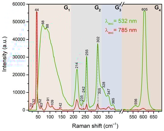
Figure 1.
Experimental Raman spectra acquired from a wurtzite cadmium sulfide (CdS) single crystal under off-resonance (red line) and near-resonance (green line) conditions. The dotted vertical lines correspond to the phonon modes at the Brillouin zone center.
The G1 region corresponds to low-frequency phonons. As seen in Figure 1, the spectrum obtained under off-resonance condition shows multiple low-intensity peaks, except for a peak located at 44 cm−1, whose signal intensity is so high that it exceeds the maximum capacity of the detector. As a result, the upper part of this peak appears flattened or “clipped.” This behavior is of technical origin, as a high laser power was required to obtain the spectrum to compensate for the low Raman cross-section and the high dispersion of the diffraction grating. In contrast, the spectrum obtained under near-resonance conditions exhibits a very broad band, with intensity maxima located at 68 and 88 cm−1.
The G2 region is characterized by phonon modes whose frequencies are located at the center of the Brillouin zone in the crystal’s reciprocal space [,]. Figure 1 shows that the intensity of the peaks in the G2 region is much more pronounced under near-resonance excitation compared to the off-resonance spectrum.
The G3 region shows a composite set of peaks originating from multiphonon scattering processes []. The spectra in Figure 1 suggest that, under near-resonance conditions, this multiphonon scattering region is more pronounced, displaying a well-defined structure with higher intensities compared to the off-resonance spectrum.
The G4 region contains a high-order phonon mode, which appears more clearly under near-resonance excitation. In this condition, the peak at 605 cm−1 shown in Figure 1 is so intense that it also exhibits a “clipped” effect. In contrast, the off-resonance spectrum shows a significantly reduced intensity for this high-order phonon. It is worth mentioning that the excitation laser used near-resonance had a relatively low power. Nevertheless, despite the dispersion effects from the diffraction grating, the signal intensity was extremely high, confirming the increase in the Raman cross-section.
In this study we will focus on analyzing the low-frequency phonon modes, identified as G1 in Figure 1. This is an area of interest due to the considerable changes observed in the spectra: the spectrum acquired under off-resonance condition shows multiple peaks that require detailed characterization, whereas the Raman spectrum obtained under near-resonance condition displays a single, intense, and broadened peak that spans almost the entire spectral region. The remaining spectral regions (G2 to G4), where the most prominent variation appears to be in phonon intensity, will be the subject of detailed analysis in future studies.
4. Discussion
4.1. Crystal Structure and Active Phonon Modes in Wurtzite CdS
In its bulk form, CdS typically adopts a hexagonal crystal structure known as wurtzite. A schematic diagram of the wurtzite CdS crystal structure, along with its lattice parameters, is shown in Figure 2a. This structure consists of alternating planes of tetrahedrally coordinated Cd2+ and S2− ions, stacked along the c-axis. A notable structural feature of CdS is its polarity, where the oppositely charged ions induce a dipole moment.
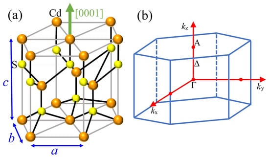
Figure 2.
(a) Schematic diagram of the crystal structure of CdS in the wurtzite form. Different colored spheres represent Cd2+ and S2− ions. The lattice parameters are a = b = 4.1 Å and c = 6.7 Å, and the green arrow indicates the [0001] direction, parallel to the c-axis. (b) First Brillouin zone of wurtzite: Γ and A are the center and edge points of the zone, respectively. Δ is the high-symmetry direction along the kz vector.
On the other hand, in the Raman scattering process in crystalline materials, both the energy and the wave vector k are conserved. This implies that only phonons with wave vector k ≈ 0 participate in the Raman scattering process. The conservation of k (or linear momentum) results in a single phonon line with a Lorentzian spectral shape, and the photon–phonon interaction is limited to the center of the Brillouin zone (representation of the primitive cell in reciprocal space). Figure 2b shows the well-known hexagonal prism of the wurtzite Brillouin zone. The center of the zone is represented by the Γ point, which is connected to point A at the edge of the zone along the Δ direction. This direction is parallel to the illumination used in our experiment.
According to the literature, the wurtzite crystal structure belongs to the space group P63mc (), with four atoms per unit cell. Hence, group theory predicts that the zone-center optical modes are A1, 2B1, E1, and 2E2. The A1 and E1 modes, along with the two E2 modes, are Raman active, while the B modes are silent. As already mentioned, wurtzite CdS is a polar semiconductor. Therefore, long-range Coulomb interactions split the A1 and E1 modes into longitudinal (LO) and transverse (TO) optical phonon modes. Thus, six phonon modes at the zone center (2A1 + 2E1 + 2E2) are active in the Raman spectra. The main Raman peaks have been assigned as follows: = 235 cm−1, = 302 cm−1, = 242 cm−1, = 305 cm−1, = 44 cm−1, and = 255 cm−1 [,,,].
The frequency values of each of these phonon modes are represented in Figure 1 by dotted vertical lines. The intensity of these peaks depends on the scattering cross-section of these phonon modes, and theory predicts an increase in scattering intensities as the energy of the exciting radiation approaches the energy band gap of the material. It can be observed in Figure 1, where the off-resonance Raman spectrum was obtained by excitation with 785 nm (red line) and the near-resonance spectrum with 532 nm (green line).
4.2. Off-Resonance Raman Peak Fitting Result
In order to identify the phonon modes present in the spectra, a peak fitting analysis was performed. Figure 3 shows the experimental Raman spectrum measured with the 785 nm excitation wavelength (open circles). This spectrum is dominated by an intense peak centered at 44 cm−1, which has been identified with the phonon mode from the wurtzite CdS. The frequency and high intensity of this peak agree with those reported in the literature for CdS [,].
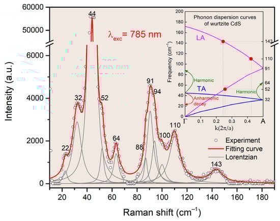
Figure 3.
Experimental off-resonance Raman spectrum (open circles) of a wurtzite CdS single crystal. The gray curves represent the phonon modes identified using Lorentzian functions, and the red line shows the best fit obtained. The inset shows the low-frequency phonon dispersion curves.
A Lorentzian line–fit analysis of the Raman spectrum shown in Figure 3 was carried out, indicating that the spectrum is composed of 10 additional peaks. The best fit for the experimental data is shown in the same figure with a red line. There is excellent agreement between the experimental data and the fit obtained. To provide a detailed description of each phonon present in the Raman spectrum, we utilized the phonon dispersion curves reported for CdS [,,]. Since the studied phonons exhibit low frequencies, the dispersion curves correspond to the transverse acoustic (TA) and longitudinal acoustic (LA) phonon modes. These curves are displayed as an inset in Figure 3, where the horizontal axis represents the magnitude of the wave vector k (in units of 2π/a). The Γ point corresponds to k = 0 (zone center) while the A point corresponds to k = 0.5 (zone edge). In the inset of Figure 3, the transverse acoustic (TA) and longitudinal acoustic (LA) branches in the wurtzite structure appear folded as a consequence of the structural equivalence between the [0001] stacking direction in wurtzite and the [111] direction in two consecutive zinc-blende unit cells [].
Thus, the following Raman peaks were identified and are described below. The peak at 22 cm−1 is the lowest frequency and corresponds exactly to half the phonon mode at 44 cm−1 in the zone center. The phonon mode with an energy of 44 cm−1 can decay into two identical acoustic phonons with energies of 22 cm−1 and opposite momenta, in accordance with the Klemens model []. Therefore, we interpret this phonon as originating from the anharmonic decay of the mode. This behavior is illustrated by a red curved arrow in the inset of Figure 3. The peak at 32 cm−1 has a frequency that coincides with that of the transverse acoustic (TA) mode located at the zone edge. The dispersion curve predicts this phonon, designated as A3 []. However, to the best of our knowledge, this is the first time it has been demonstrated experimentally. The peak at 52 cm−1 can be considered as a zone-middle mode. We propose that this mode originates from the longitudinal acoustic (LA) branch at k ≈ 0.25, as shown in the inset of Figure 3.
Continuing with the analysis, the peak at 64 cm−1 has exactly twice the frequency of the aforementioned A3 phonon mode, which is why we consider it to be its harmonic, which is 2A3. This is illustrated in the inset of Figure 3 with a green curved arrow in the zone edge. Similarly, the peak at 88 cm−1 is interpreted as a harmonic mode or overtone, corresponding to . In Raman spectroscopy, overtones arise from higher-order scattering processes and are observed at integer multiples of the fundamental phonon frequency []. Again, in the inset of Figure 3, but now located in the zone center, a green curved arrow is used to describe this phonon mode. A similar interpretation was previously proposed in reference [], although in their case the assignment was made for CdS nanowires. The peak at 91 cm−1 corresponds exactly to the value of the LA phonon mode in the zone edge, where the two dispersion curves of the LA mode converge (inset in Figure 3). This generates a notable intensity of this mode in the frequency range analyzed. This phonon has also been observed in CdS platelets []. In addition, the proximity of this mode with the frequencies at 94 and 100 cm−1 produces the widening of this band observed in the experimental data. These frequencies correspond to k ≈ 0.5 values in the edge zone. Finally, the peaks at 110 (≈52 + 64) and 143 (52 + 91) cm−1 have been assigned to combinations (sum modes) of acoustic phonons at the zone edge []. However, we consider that these phonons may correspond to values of k ≈ 0.4 and k ≈ 0.24, respectively. The above is shown in the inset of Figure 3, and its physical origin is due to the breakdown of sealing rules. The relaxation of this strict selection rule for k ≈ 0 occurs when a loss of periodicity is introduced in the crystal. This loss allows phonons with k ≠ 0 to couple with light, thereby contributing to the Raman spectrum.
4.3. Near-Resonance Raman Peak Fitting Result
Figure 4 shows the experimental Raman spectrum measured with the 532 nm excitation wavelength (open circles). The data does not display any peak below 40 cm−1. Above this frequency, the signal intensity increases significantly, forming a broad band that appears to be composed of multiple peaks. This band extends across the entire analyzed spectral range, with a less intense tail observed below 200 cm−1. The data were fitted with multiple Lorentzian peaks to determine the Raman frequencies and intensities for each individual phonon mode. The best fit for the experimental data is shown with a red line in Figure 4. There is excellent agreement between the experimental data and the fit obtained, which is described below.
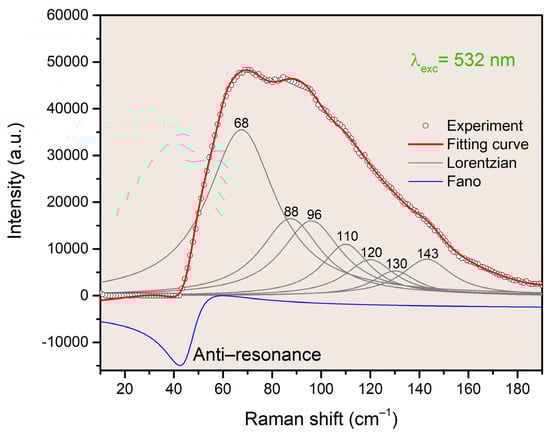
Figure 4.
Experimental near-resonance Raman spectrum (open circles) of a wurtzite CdS single crystal. The gray curves represent the phonon modes identified using Lorentzian functions, the blue line is a Fano-type curve, and the red line shows the best fit obtained.
As noted earlier, the Raman scattering cross-section increases significantly as the excitation energy approaches the material’s band gap. In contrast, previous studies on CdS have reported a significant decrease in the intensity of the nonpolar phonon mode when the excitation laser energy is near, but slightly below, the crystal’s band gap energy [,]. This phenomenon, known as antiresonance, results from destructive interference between resonant and non-resonant contributions to the Raman scattering amplitudes []. Consequently, we initiated our analysis by modeling the previously described antiresonance with a Fano-type curve, shown as a blue line in Figure 4. To the best of our knowledge, this is the first time that a Fano-type curve has been used to describe the observed low-frequency antiresonance in CdS.
The Fano-type line shape arises from the coupling between discrete and continuum states. In Raman spectroscopy, this interaction originates from the overlap in energy between photoexcited electrons—undergoing transitions within the continuum of electronic states—and discrete phonon scattering processes.
In CdS, cadmium vacancies (VCd) act as deep acceptors capable of trapping electrons. The VCd defect level lies approximately 1.10 eV above the valence-band maximum, as illustrated in Figure 5 [].
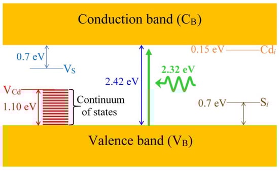
Figure 5.
Schematic energy level diagram for different transitions in CdS. Notation: cadmium vacancy (VCd), sulfur vacancy (VS), interstitial cadmium (Cdi), interstitial sulfur (Si); the blue double arrow is the band gap and the green arrow is the incident photon.
These vacancies can form a continuum of electronic states that are accessible to photoexcited electrons generated by an excitation energy of 2.32 eV. The energy of these photoexcited electrons can readily overlap with the phonon mode, which has an energy of about 5.46 meV. The interference between the electronic continuum and the discrete phonon gives rise to the characteristic Fano-type interaction.
The Fano-type line shape is given as follows []:
where the term , also called a reduced energy variable, is equal to , I0 is a factor for the scattering intensity of the peak, q is the asymmetry parameter, Γ is the Raman line width, ω is the frequency, and ω0 is the phonon frequency. The values used to generate the blue curve shown in Figure 4 were I0 = −2990, q = −2, ω0 =46, and Γ = 14.
The Fano-type curve has its anti-resonance at 46 cm−1 due to ω0 = ω + Γ/, where ω is the uncoupled phonon mode frequency []. To reproduce the intense broadband, we employed Lorentzian functions at 68, 88, 96, 110, 120, 130, and 143 cm−1. Some of these frequencies coincide with or are in close proximity to values previously used to fit the Raman spectrum acquired off-resonance. However, the Lorentzian functions utilized for the near-resonance Raman spectrum are considerably broader compared to those used off-resonance. This can be explained by considering the increased Raman scattering cross-section.
5. Conclusions
In this work, we investigated the low-frequency phonon modes in wurtzite cadmium sulfide (CdS) single crystals using Raman spectroscopy under off- and near-resonance conditions. Our results provide new experimental insights into phonon modes that have been previously underexplored, particularly in the spectral region below the fundamental longitudinal optical (LO) phonon. Under off-resonance conditions, several low-intensity peaks were identified and assigned to both zone-edge and zone-center acoustic phonons, some of which had not been previously confirmed experimentally. Several of the identified phonons have their origin in the breakdown of the strict momentum selection rules due to lattice disorder or symmetry breaking. In addition, anharmonic decay processes and harmonic contributions were detected.
In near-resonance conditions, the Raman spectrum exhibited a pronounced broadband feature with an antiresonance component, which we successfully modeled using a Fano-type function—representing, to the best of our knowledge, the first such modeling applied to low-frequency antiresonance in CdS. The broad Lorentzian components required to reproduce this spectrum suggest an enhanced photon–phonon interaction due to resonance effects.
These findings highlight the complex behavior of low-frequency phonons in CdS and demonstrate how their spectral characteristics evolve between off- and near-resonance regimes. This study not only fills a gap in the current understanding of CdS vibrational properties but also provides a methodological framework for future investigations of phonon dynamics in semiconductors. The detailed characterization of low-frequency phonons may have implications for improving thermal management and charge transport in CdS-based optoelectronic and thermoelectric devices.
Author Contributions
Conceptualization, C.I.M.R. and R.C.; methodology, C.I.M.R.; formal analysis, C.I.M.R., R.C., J.R.S.E., J.C.C., F.G.P.L., and J.M.M.; investigation, C.I.M.R., R.C., J.R.S.E., J.C.C., F.G.P.L., and J.M.M.; writing—original draft preparation, C.I.M.R., R.C., J.R.S.E., J.C.C., F.G.P.L., and J.M.M.; writing—review and editing, C.I.M.R., R.C., J.R.S.E., J.C.C., F.G.P.L., and J.M.M. All authors have read and agreed to the published version of the manuscript.
Funding
This research received no external funding. The article processing charge was covered through project 282877 of the “Programa Apoyo a Mejora en Condiciones D Producción D Personas integrantes DL SNII y SNCA (PROSNII 2025)” of the Universidad de Guadalajara.
Data Availability Statement
The original contributions presented in the study are included in the article; further inquiries can be directed to the corresponding author.
Conflicts of Interest
The authors declare no conflicts of interest.
References
- He, B.; Zhang, W. II–VI semiconductors and their device applications. In Handbook of Chalcogen Chemistry: New Perspectives in Sulfur, Selenium and Tellurium, 1st ed.; Devillanova, F., Du Mont, W.W., Eds.; RSC Publishing: Cambridge, UK, 2013; Volume 2; pp. 180–231. [Google Scholar] [CrossRef]
- Meher, S.R.; Kaushik, D.K.; Subrahmanyam, A. Native defects in sol–gel derived CdS buffer layers for photovoltaic applications. J. Mater. Sci. Mater. Electron. 2017, 28, 6033–6046. [Google Scholar] [CrossRef]
- Faraj, M.G.; Sabri, M.M.; Hamad, N.H. Photoelectrochemical investigations of cadmium sulfide-doped silver (CdS) on flexible substrates. J. Mater. Sci. Mater. Electron. 2024, 35, 710. [Google Scholar] [CrossRef]
- Pan, A.; Zhu, X. Optoelectronic properties of semiconductor nanowires. In Semiconductor Nanowires, 1st ed.; Arbiol, J., Xiong, Q., Eds.; Woodhead Publishing: Cambridge, UK, 2015; Volume 2; pp. 327–363. [Google Scholar] [CrossRef]
- Ahmad, N.I.; Kar, Y.B.; Doroody, C.; Kiong, T.S.; Rahman, K.S.; Harif, M.N.; Amin, N. A comprehensive review of flexible cadmium telluride solar cells with back surface field layer. Heliyon 2023, 9, e21622. [Google Scholar] [CrossRef]
- Saxena, N.; Kalsi, T.; Kumar, P. CdS-based photodetectors for visible-UV spectral region. In Handbook of II-VI Semiconductor-Based Sensors and Radiation Detectors, 1st ed.; Korotcenkov, G., Ed.; Springer Nature: Heidelberg, Germany, 2023; Volume 2; pp. 251–279. [Google Scholar] [CrossRef]
- Murai, H.; Abe, T.; Matsuda, J.; Sato, H.; Chiba, S.; Kashiwaba, Y. Improvement in the light emission characteristics of CdS: Cu/CdS diodes. Appl. Surf. Sci. 2005, 244, 351–354. [Google Scholar] [CrossRef]
- Zhang, Y.; Pham, X.M.; Keating, T.; Jia, N.; Mullen, A.; Laishram, D.; Gao, M.Y.; Corbett, B.; Liu, P.; Sun, X.W.; et al. Highly efficient inverted light-emitting diodes based on vertically aligned CdSe/CdS nanorod layers fabricated by electrophoretic deposition. ACS Appl. Mater. Interfaces 2024, 16, 10459–10467. [Google Scholar] [CrossRef]
- Channei, D.; Chansaenpak, K.; Jannoey, P.; Phanichphant, S. The staggered heterojunction of CeO2/CdS nanocomposite for enhanced photocatalytic activity. Solid State Sci. 2019, 96, 105951. [Google Scholar] [CrossRef]
- Ma, L.; Ai, X.; Wu, X. Effect of substrate and Zn doping on the structural, optical and electrical properties of CdS thin films prepared by CBD method. J. Alloys Compd. 2017, 691, 399–406. [Google Scholar] [CrossRef]
- Alam, A.; Kumar, S.; Singh, D.K. Cadmium sulphide thin films deposition and characterization for device applications. Mater. Today Proc. 2022, 62, 6102–6106. [Google Scholar] [CrossRef]
- Najm, A.S.; Naeem, H.S.; Alabboodi, K.O.; Hasbullah, S.A.; Hasan, H.A.; Holi, A.M.; AL-Zahrani, A.A.; Sopian, K.; Bais, B.; Majdi, H.S.; et al. New systematic study approach of green synthesis CdS thin film via Salvia dye. Sci. Rep. 2022, 12, 12521. [Google Scholar] [CrossRef]
- Regmi, A.; Basnet, Y.; Bhattarai, S.; Gautam, S.K. Cadmium sulfide nanoparticles: Synthesis, characterization, and antimicrobial study. J. Nanomater. 2023, 2023, 8187000. [Google Scholar] [CrossRef]
- Hadi, I.H.; Khashan, K.S.; Sulaiman, D. Cadmium sulphide (CdS) nanoparticles: Preparation and characterization. Mater. Today Proc. 2021, 42, 3054–3056. [Google Scholar] [CrossRef]
- Kim, S.; Kim, S.; Oh, H.; Choi, W.I.; Lim, J.M. Large-scale continuous synthesis of CdS quantum dots using an impinging jet mixer. Colloids Surf. A 2024, 703, 135202. [Google Scholar] [CrossRef]
- Kandasamy, K.; Surendhiran, S.; Jagan, K.S.G.; Kumar, G.S.; Khadar, Y.S.; Rajasingh, P. Green synthesis of CdS Quantum dots for photocatalytic and anti-corrosive applications in aqueous media. Appl. Surf. Sci. Adv. 2023, 13, 100364. [Google Scholar] [CrossRef]
- Das, S.; Ahn, Y.H. Synthesis and application of CdS nanorods for LED-based photocatalytic degradation of tetracycline antibiotic. Chemosphere 2022, 291, 132870. [Google Scholar] [CrossRef] [PubMed]
- Qi, Z.; Chen, J.; Li, Q.; Wang, N.; Carabineiro, S.A.; Lv, K. Increasing the photocatalytic hydrogen generation activity of CdS nanorods by introducing interfacial and polarization electric fields. Small 2023, 19, 2303318. [Google Scholar] [CrossRef]
- Hu, H.; Zhou, J.; Miao, Z.; Zhu, H.; Wang, C.; Lin, L. Catalytic Growth of CdS Nanowires by Microplasma-Prepared Gold Nanoparticles. Ind. Eng. Chem. Res. 2025, 64, 502–510. [Google Scholar] [CrossRef]
- Sarangi, S.N.; Sahu, S.N.; Nozaki, S. CdS nanowires formed by chemical synthesis using conjugated single-stranded DNA molecules. Phys. E 2018, 97, 64–68. [Google Scholar] [CrossRef]
- Ghasempour, A.; Dehghan, H.; Ataee, M.; Chen, B.; Zhao, Z.; Sedighi, M.; Guo, X.; Shahbazi, M.A. Cadmium sulfide nanoparticles: Preparation, characterization, and biomedical applications. Molecules 2023, 28, 3857. [Google Scholar] [CrossRef]
- Vadakkedath Gopi, S.; Spalatu, N.; Basnayaka, M.; Krautmann, R.; Katerski, A.; Josepson, R.; Grzibovskis, R.; Vembris, A.; Krunks, M.; Oja Acik, I. Post deposition annealing effect on properties of CdS films and its impact on CdS/Sb2Se3 solar cells performance. Front. Energy Res. 2023, 11, 1162576. [Google Scholar] [CrossRef]
- Sivagamai, D.; Priyadarshini, B.G. Composition dependent structural, morphological, optical and electrical properties of CdS: Co window layer grown by chemical bath deposition. Mater. Sci. Energy Technol. 2020, 3, 709–718. [Google Scholar] [CrossRef]
- Xie, S.; Zhu, H.; Zhang, X.; Wang, H. A brief review on the recent development of phonon engineering and manipulation at nanoscales. Int. J. Extreme Manuf. 2024, 6, 012007. [Google Scholar] [CrossRef]
- Jones, R.R.; Hooper, D.C.; Zhang, L.; Wolverson, D.; Valev, V.K. Raman techniques: Fundamentals and frontiers. Discov. Nano 2019, 14, 231. [Google Scholar] [CrossRef]
- Schmitt, M.; Popp, J. Raman spectroscopy at the beginning of the twenty-first century. J. Raman Spectrosc. 2006, 37, 1508–1511. [Google Scholar] [CrossRef]
- Zaretskaya, E.P.; Gremenok, V.P.; Buskis, K.P.; Korolik, O.V.; Pashanyan, S.T.; Tokmajyan, A.S.; Musayelyan, A.S.; Petrosyan, S.G. Microstructure and Raman scattering of CdS films obtained by chemical deposition. J. Appl. Spectrosc. 2024, 91, 25–30. [Google Scholar] [CrossRef]
- Ashok, A.; Regmi, G.; Romero-Núñez, A.; Solis-López, M.; Velumani, S.; Castaneda, H. Comparative studies of CdS thin films by chemical bath deposition techniques as a buffer layer for solar cell applications. J. Mater. Sci. Mater. Electron. 2020, 31, 7499–7518. [Google Scholar] [CrossRef]
- Dzhagan, V.M.; Valakh, M.Y.; Himcinschi, C.; Milekhin, A.G.; Solonenko, D.; Yeryukov, N.A.; Raevskaya, O.E.; Stroyuk, O.L.; Zahn, D.R. Raman and infrared phonon spectra of ultrasmall colloidal CdS nanoparticles. J. Phys. Chem. C 2014, 118, 19492–19497. [Google Scholar] [CrossRef]
- Prabhu, R.R.; Abdul Khadar, M. Study of optical phonon modes of CdS nanoparticles using Raman spectroscopy. Bull. Mater. Sci. 2008, 31, 511–515. [Google Scholar] [CrossRef]
- Ahmed, B.; Kumar, S.; Kumar, S.; Ojha, A.K. Shape induced (spherical, sheets and rods) optical and magnetic properties of CdS nanostructures with enhanced photocatalytic activity for photodegradation of methylene blue dye under ultra-violet irradiation. J. Alloys Compd. 2016, 679, 324–334. [Google Scholar] [CrossRef]
- Kumar, P.; Saxena, N.; Chandra, R.; Gupta, V.; Agarwal, A.; Kanjilal, D. Nanotwinning and structural phase transition in CdS quantum dots. Discov. Nano 2012, 7, 584. [Google Scholar] [CrossRef] [PubMed]
- Saleem, M.F.; Zhang, H.; Deng, Y.; Wang, D. Resonant Raman scattering in nanocrystalline thin CdS film. J. Raman Spectrosc. 2016, 48, 224–229. [Google Scholar] [CrossRef]
- Leite, R.C.C.; Scott, J.F.; Damen, T.C. Multiple-phonon resonant Raman scattering in CdS. Phys. Rev. Lett. 1969, 22, 780. [Google Scholar] [CrossRef]
- Fan, H.M.; Ni, Z.H.; Feng, Y.P.; Fan, X.F.; Kuo, J.L.; Shen, Z.X.; Zou, B.S. Anisotropy of electron-phonon coupling in single wurtzite CdS nanowires. Appl. Phys. Lett. 2007, 91, 171911. [Google Scholar] [CrossRef]
- Hu, C.; Zeng, X.; Cui, J.; Chen, H.; Lu, J. Size effects of Raman and photoluminescence spectra of CdS nanobelts. J. Phys. Chem. C 2013, 117, 20998–21005. [Google Scholar] [CrossRef]
- Tell, B.; Damen, T.C.; Porto, S.P.S. Raman effect in cadmium sulfide. Phys. Rev. 1966, 144, 771. [Google Scholar] [CrossRef]
- Arguello, C.A.; Rousseau, D.L.; Porto, S.D.S. First-order Raman effect in wurtzite-type crystals. Phys. Rev. 1969, 181, 1351. [Google Scholar] [CrossRef]
- Nusimovici, M.A.; Birman, J.L. Lattice dynamics of wurtzite: CdS. Phys. Rev. 1967, 156, 925. [Google Scholar] [CrossRef]
- Grünwald, M.; Zayak, A.; Neaton, J.B.; Geissler, P.L.; Rabani, E. Transferable pair potentials for CdS and ZnS crystals. J. Chem. Phys. 2012, 136, 234111. [Google Scholar] [CrossRef]
- Iqbal, M.F.; Saeed, S.; Wu, L.; Zhu, P.; Wang, D. Enhanced anharmonic phonon coupling and decay dominated by low-energy phonons in CdS nanowires. J. Raman Spectrosc. 2019, 50, 1492–1501. [Google Scholar] [CrossRef]
- Chi, T.T.K.; Gouadec, G.; Colomban, P.; Wang, G.; Mazerolles, L.; Liem, N.Q. Off-resonance Raman analysis of wurtzite CdS ground to the nanoscale: Structural and size-related effects. J. Raman Spectrosc. 2011, 42, 1007–1015. [Google Scholar] [CrossRef]
- Fan, Z.; Koster, R.S.; Wang, S.; Fang, C.; Yalcin, A.O.; Tichelaar, F.D.; Zandbergen, H.W.; van Huis, M.A.; Vlugt, T.J. A transferable force field for CdS-CdSe-PbS-PbSe solid systems. J. Chem. Phys. 2014, 141, 244503. [Google Scholar] [CrossRef]
- Prasad, N.; Karthikeyan, B. Resonant and Off-Resonant Phonon Properties of Wurtzite ZnS: Effect of Morphology on Fröhlich Coupling and Phonon Lifetime. J. Phys. Chem. C 2018, 122, 18117–18123. [Google Scholar] [CrossRef]
- Beserman, R. Zone edge phonons in CdS1−xSex. Solid State Commun. 1977, 23, 323–327. [Google Scholar] [CrossRef]
- Scott, J.F.; Damen, T.C.; Leite, R.C.C.; Shah, J. Light Scattering from Plasmas and Single-Particle Excitations in Cadmium Sulfide near Resonance. Phys. Rev. B 1970, 1, 4330. [Google Scholar] [CrossRef]
- Ralston, J.M.; Wadsack, R.L.; Chang, R.K. Resonant cancelation of Raman scattering from CdS and Si. Phys. Rev. Lett. 1970, 25, 814. [Google Scholar] [CrossRef]
- Varley, J.B.; Lordi, V. Electrical properties of point defects in CdS and ZnS. Appl. Phys. Lett. 2013, 103, 102103. [Google Scholar] [CrossRef]
- Kumar, A.; Rambadey, O.V.; Rai, H.; Sagdeo, P.R. Role of Laser Excitation Wavelength and Power in Fano Resonance Scattering in RFe0.50Cr0.50O3 (R = Sm, Er, and Eu): A Brief Raman Study. J. Phys. Chem. C 2022, 126, 5403–5410. [Google Scholar] [CrossRef]
- Wu, J.B.; Lin, M.L.; Cong, X.; Liu, H.N.; Tan, P.H. Raman spectroscopy of graphene-based materials and its applications in related devices. Chem. Soc. Rev. 2018, 47, 1822–1873. [Google Scholar] [CrossRef]
Disclaimer/Publisher’s Note: The statements, opinions and data contained in all publications are solely those of the individual author(s) and contributor(s) and not of MDPI and/or the editor(s). MDPI and/or the editor(s) disclaim responsibility for any injury to people or property resulting from any ideas, methods, instructions or products referred to in the content. |
© 2025 by the authors. Licensee MDPI, Basel, Switzerland. This article is an open access article distributed under the terms and conditions of the Creative Commons Attribution (CC BY) license (https://creativecommons.org/licenses/by/4.0/).