1. Introduction
Lead halide perovskites, incorporating organic cations such as methylammonium (MA
+), have emerged as versatile semiconductors with applications spanning photovoltaics, light emission, and radiation detection [
1,
2,
3,
4]. A combination of tunable band gaps, high absorption coefficients, long carrier diffusion lengths, and solution processability has made them particularly attractive for next generation of photovoltaics [
4,
5,
6,
7]. In recent years, these properties have also driven growing interest in the use of perovskites for space energy harvesting [
5,
8,
9] and dosimetry in medical contexts, including radiotherapy monitoring [
10,
11,
12].
Despite these advantages, hybrid organic-inorganic perovskites remain notoriously unstable under environmental factors such as moisture, oxygen, and heat, as well as external stimuli including light and radiation. Exposure to moisture, oxygen, and elevated temperatures leads to decomposition and irreversible loss of performance [
13,
14]. Even more critically for space and medical applications, their intrinsic sensitivity to ionizing radiation introduces additional degradation pathways [
8,
15,
16,
17,
18]. Understanding how different forms of radiation interact with perovskite lattices is thus essential for both fundamental insight and device reliability.
Electron irradiation is not an artificial test condition; it is one of the dominant degradation factors in both space and medical environments. While humidity and thermal stress affect perovskites through chemical decomposition, high-energy electrons create dense electronic excitations that can trigger defect formation through non-radiative recombination, ion migration, and radiolysis of organic cations. These degradation pathways, rather than ballistic atom displacement, define the radiation response of halide perovskites. However, how these processes depend on absorber thickness and electron energy remains unclear. This motivates the present study.
In this work, we focus on MAPbI
3 because it remains the most representative and extensively studied member of the hybrid lead-halide perovskite family [
19,
20,
21,
22]. Its status as a model system provides a reliable basis for examining electronic and radiation-induced processes, supported by a large body of experimental and theoretical data [
23,
24,
25,
26,
27]. This makes MAPbI
3 a suitable platform for extracting mechanistic insights that are relevant to the broader class of lead-halide perovskites, and it establishes a foundation on which comparative studies can be built.
In space, perovskites may encounter energetic electron fluxes from the Van Allen belts [
28,
29] and solar events [
30,
31], while in dosimetry, they are exposed to therapeutic electron beams [
32]. Unlike heavy particles, which predominantly damage materials via direct ballistic collisions, electron irradiation deposits energy primarily through ionization and electronic excitation. The resulting nonequilibrium carrier populations can relax via multiple channels, including exciton self-trapping, Auger processes, and radiative or non-radiative recombination [
8,
15,
18]. Crucially, the decay of these excitations may couple to the lattice, leading to defect generation indirectly, rather than through a direct displacement mechanism [
26,
33,
34].
Among the most probable outcomes of such relaxation are halide vacancies, particularly iodine vacancies, which are known to act as efficient nonradiative recombination centers and can severely compromise device performance [
35,
36]. This mode of defect formation highlights the complexity of electron–matter interactions in perovskites, where defect chemistry is controlled as much by electronic pathways as by structural features.
The sequence of processes (ionization, electronic excitation and so on) and the relaxation pathways that can lead to defect formation are still not fully understood, particularly in how it depend on electron energy. At lower energies (tens to hundreds of keV), secondary electron cascades dominate, while at higher energies (MeV scale) multiple ionization and deep electronic excitations become significant [
37,
38]. The determination of these processes is important to identify the microscopic origins of radiation damage and to guide the design of more resistant perovskite devices. In this study, we explore the radiation effects in MAPbI
3 under electron irradiation via Monte Carlo simulations.
2. Calculation Details
To gain deeper insight into electron–matter interaction mechanisms in lead-halide perovskites, we carried out Monte Carlo simulations for MAPbI3 across a wide range of electron energies. The purpose of these simulations was to quantify ionization, the generation and transport of secondary electrons, and depth-dependent energy deposition profiles, and to relate these processes to possible defect-formation pathways.
We selected MAPbI3 as the model system because its structural, electronic, and radiation-response properties are among the most comprehensively documented, making it the standard reference compound within the perovskite family. This allows the simulation to rely on well-established material parameters rather than uncertain or extrapolated values.
Simulations were performed for uniform monoenergetic electron fluxes with primary energies from 100 keV to 100 MeV, covering the regimes relevant both for space environments and therapeutic electron sources. Four absorber thicknesses were considered (10 μm, 100 μm, 1 mm, and 1 cm). Although operational solar-cell layers are of the order of 500 nm, thicker slabs substantially increase the interaction volume and thereby improve statistics for rare processes such as the initiation of electron cascades. Thicknesses in the tens–hundreds of micrometers are also relevant for dosimetric applications [
12,
39].
All calculations were carried out using the Geant4 toolkit [
40,
41]. In this framework, particle transport is described by a combination of elastic scattering, inelastic electron interactions, ionization, bremsstrahlung, and the production and propagation of secondary electrons. These processes represent the dominant electronic energy-loss channels responsible for radiation-induced electronic excitations in perovskites. Nuclear displacement interactions are not explicitly included, which is consistent with the fact that electron-induced damage in this energy range is primarily electronic rather than ballistic in nature [
42].
The material was defined in the DetectorConstruction class using its full atomic composition (elemental species, atomic numbers and atomic masses), stoichiometric ratios, bulk density, and sample geometry. These definitions ensure that the electron trajectories, scattering cross-sections, and resulting cascades are computed based on the actual chemical and elemental makeup of MAPbI3 rather than on an abstract or generic absorber.
Geant4 allows particle fluxes up to 9.9 × 10⁹ particles/cm2, but extremely high-intensity simulations become computationally prohibitive. Since the number of potential interaction events scales with absorber thickness, increasing the thickness from 0.5 μm to 1 cm enhances the event count by a factor of ~2 × 10⁶. Consequently, a 1 cm target irradiated with 105 particles/cm2 produces a comparable number of interactions to a 500 nm film exposed to ~1011 particles/cm2, enabling statistically meaningful analysis without impractical computational cost.
The PrimaryGeneratorAction class defined source parameters (position, energy, and number of incident particles). Energy deposition was tracked in the SteppingAction class, using GetTotalEnergyDeposit for total absorbed energy and GetNonIonizingEnergyDeposit for non-ionizing losses.
Monte Carlo simulations were carried out using Geant4 (v11.3.2) with a custom PhysicsList class based on G4EmStandardPhysicsWVI to assess the electromagnetic processes with particles across a wide energy range (10 eV–100 MeV) accurately. It includes Rayleigh, Compton, photoelectric, ionization, multiple scattering, pair production, and bremsstrahlung processes. For e−/e+, multiple scattering was modeled with G4WentzelVIModel combined with single elastic scattering at large angles. Ionization was treated using the Lindhard–Sorensen model. The decay processes were treated via G4Decay and G4RadioactiveDecayBase. Multiple scattering was described using the G4UrbanMscModel. Additionally, Auger effect, cascades of Auger effect and fluorescence were considered via flag “True” in PhysicsList class.
Compton scattering of generated photons was modeled by using the Klein–Nishina model, which reduces to Thomson scattering at low energies and accounts for relativistic effects at high energies.
For different perovskite thicknesses, production cutoff and energy thresholds were adjusted accordingly. For 1 cm absorber, a production cutoff of 0.7 mm was applied, with thresholds of 37.4 keV for secondary photons, 504.3 keV for electrons, 482.5 keV for positrons, and 70 keV for secondary protons; for 1 mm absorber: a production cutoff of 0.07 mm was applied, with thresholds of 8.3 keV for secondary photons, 111.7 keV for electrons, 109.3 keV for positrons, 7 keV for secondary protons; for 100 μm: a production cutoff of 7 μm was applied, with thresholds of 1.8 keV for secondary photons, 27.2 keV for electrons, 26.5 keV for positrons, 0.7 keV for secondary protons; for 10 μm: a production cutoff of 0.7 μm was applied, with thresholds of 10 eV for secondary photons, 858 eV for electrons, 842 eV for positrons, 70 eV for secondary protons.
This choice provides a reasonable balance between computational efficiency and accurate transport of secondary particles, reducing the number of short steps and low-energy operations for the corresponding thickness. Importantly, lower thresholds were used in thin layers to resolve localized ionization and vacancy generation, while in thick absorbers, coarser cuts adequately capture the macroscopic energy deposition.
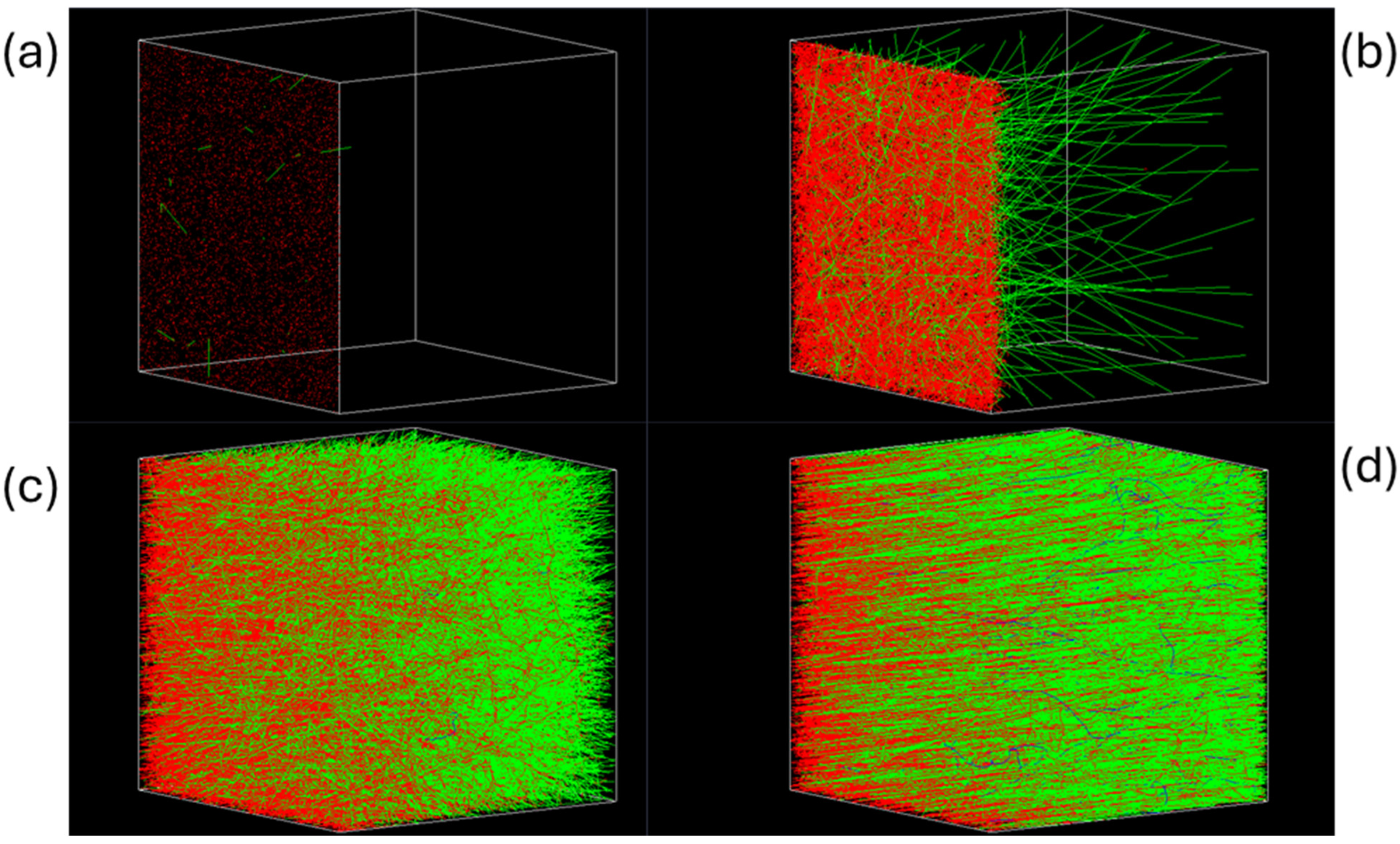
The particle transport within the simulation volume is presented in
Figure 1. It could be seen that increasing the energy not only leads to uniform irradiation of the entire volume but also causes an increase in the number of secondary γ-quanta.
Figure 1 shows how the accelerated electrons interact with matter and create secondary particles depending on the incident energy. At 0.1 MeV, electrons stop within a shallow surface region, while at 1 MeV they reach deeper into the material and generate more secondary photons. For 10 MeV, most electrons already traverse the layer and generate visible secondary photons and positrons. At 100 MeV, electrons pass almost straight through, with abundant secondary photons and positrons produced along the way. This sequence visualizes the gradual transition from surface-limited penetration to nearly complete transmission as the electron energy increases.
3. Results and Discussion
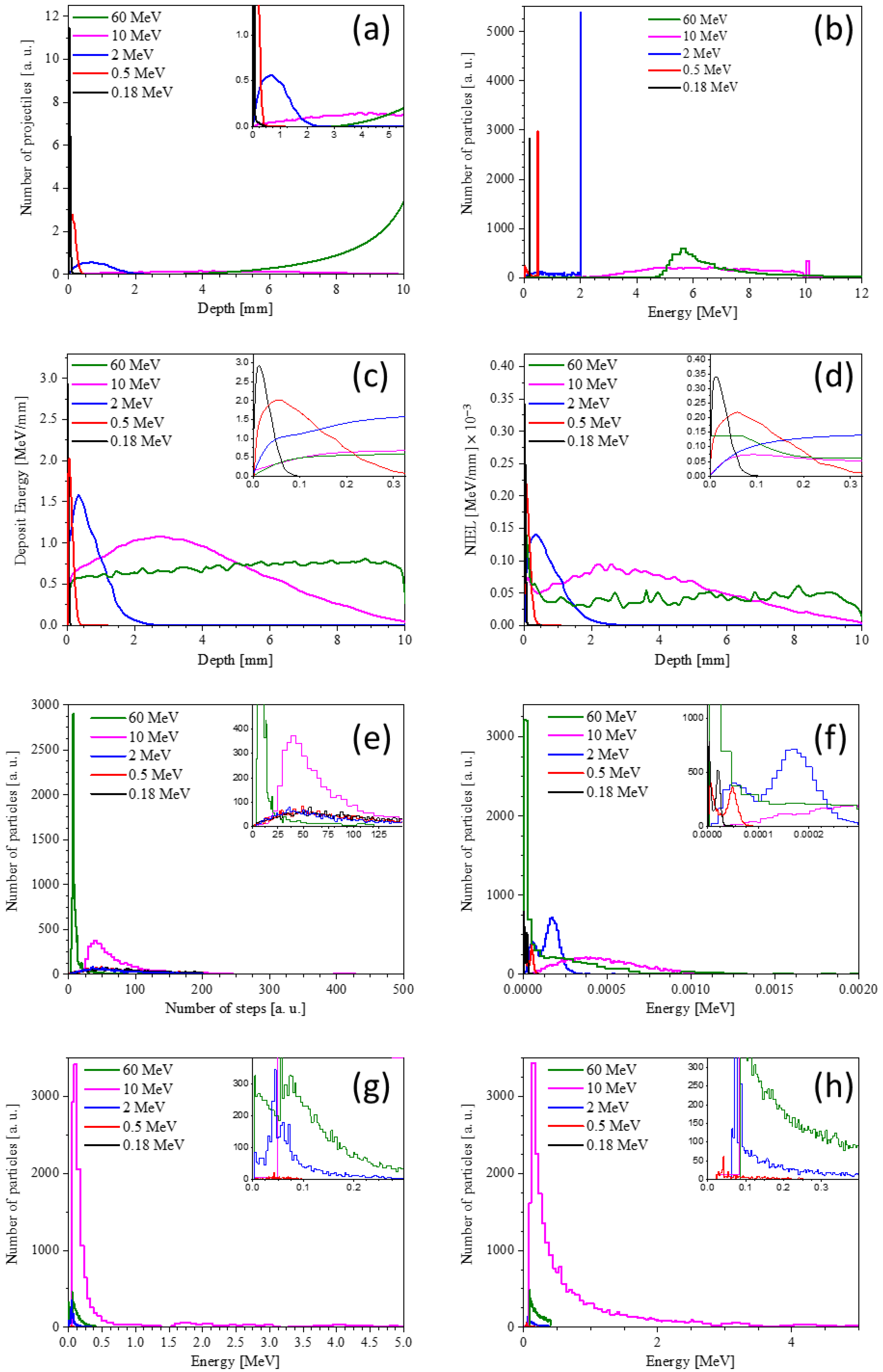
Figure 2a shows the projective paths of particles of 1 cm thick MAPbI
3. It is evident that the depth of the electron’s path depends significantly on the electron’s energy, which is in good agreement with the tracks shown in
Figure 1. In other words, electrons within certain energy ranges release their energy completely, and the region of energy release depends on the energy of the primary particles. Only particles with an energy of 60 MeV will pass through a 1 cm thick perovskite layer. Furthermore, electrons with an energy of 10 MeV have a uniform distribution of the region of complete stopping across the depth of the perovskite layer. We can assume that a significant number of electrons with energies up to 10 MeV will release energy when passing through the MAPbI
3 material, despite its small thickness.
Let us examine in more detail the depth distribution of energy deposited by electrons in a 1 cm thick perovskite layer (
Figure 2c). It is clear that the depth distribution of energy losses will vary significantly for electrons of different energies. For example, electrons with an energy of 180 keV completely release their energy in the first 100 µm. Increasing the energy to 0.5 MeV increases the most damaged range to 300 µm, but the maximum distribution still lies in the region of up to 100 µm.
High-energy electrons are effectively decelerated at significantly greater depths, meaning they can damage the entire solar panel (or detector) and perovskite layer uniformly across the entire depth. For example, the energy losses of 60 MeV electrons are homogeneously distributed throughout the layer being studied, and their absolute maximum value is four times lower than that of 0.5 MeV electrons.
We also note the interesting distribution of the number of electrons by deposited energy (
Figure 2b). While for electrons of lower energies almost all particles lose all energy (up to 2 MeV), 10 MeV electrons have a “vague” distribution with an energy minimum around 3 MeV, a plateau, and a characteristic maximum, indicating that a significant portion of the electrons still lose all their energy. The most interesting distribution is that of 60 MeV electrons, which have a maximum around 6 MeV and gradually decrease to virtually zero around 10 MeV.
Before analyzing the processes responsible for this behavior of electrons of various energies, let us consider the distribution of non-ionization losses as a function of the incident particle energy. Whereas the depth distribution (
Figure 2d) is nearly identical to that of the total energy losses, the distribution of particles by their contribution to non-ionization losses (
Figure 2f) exhibits a number of distinctive features.
Three distinct electron energy ranges can also be distinguished, each exerting a different effect on the perovskite layers. Electrons with energies of 10 MeV exhibit the highest average non-ionization losses; their distribution is an asymmetric bell-shaped curve and is apparently close to Gaussian. Electrons with energies of 60 MeV exhibit a distribution close to exponential, and a significant portion of them contribute virtually nothing to elastic interactions (there is little structural damage; the electrons pass through, expending their energy on excitation of the electron subsystem). Electrons of lower energies have a two-peak distribution of non-ionization losses, and their magnitude is determined by the energy of the incident particles and has significant indicators for electrons with an energy of 2 MeV.
Similarly, three regions can be distinguished in the distributions of the number of events occurring with primary particles (
Figure 2e). It is worth noting that electrons with an energy of 10 MeV have a noticeable peak in the region of 50 (the number of primary particles scattering events), but otherwise their dependence is similar to that of electrons of lower energies.
As expected, in all cases, the most probable process is the Coulomb interaction of incident electrons with the outer-shell electrons of the target atoms (see detailed discussion on other processes below). These processes are several orders of magnitude more probable than others, and they determine the primary inelastic energy losses of electrons. If we compare the probability of producing a secondary charged particle in a single scattering event, it is several orders of magnitude greater than the probability of producing neutral particles. Other processes that occur and can influence the overall energy loss of electrons include bremsstrahlung losses (their contribution increases with increasing primary particle energy), the photoelectric effect, and ionization.
As shown in
Figure 1, γ-quanta are more likely to leave the perovskite volume, and their average energies reach 450 keV. On the other hand, the secondary electrons that are formed have low average energies (15 keV) and do not make a significant contribution to defect formation compared to the primary particles [
43]. It should be especially noted that in the case of high-energy electrons, radiation-induced transformations of some elements begin to occur. In this case, isotopes that undergo subsequent radioactive decay are not formed [
43]. In addition, secondary protons and neutrons are formed, but their number is insufficient to cause significant radiation damage, and their energies are too low to activate the samples.
Figure 2g,h show the energy distributions of secondary charged and neutral particles. Note that irradiation with an energy of 10 MeV generates secondary particles most efficiently. Furthermore, a distinct external difference in the distribution shape of secondary charged particles is noted depending on the primary electron energy. Here, as before, three ranges can be distinguished: up to 2 MeV, 10 MeV, and 60 MeV.
Thus, different primary electron energy ranges trigger different processes in perovskite materials, and the most interesting energy range, from the standpoint of energy transfer to hybrid lead perovskites, appears to be around 10 MeV. However, it is important to note that electrons with energies of 2 MeV will also have a significant effect on perovskite materials.
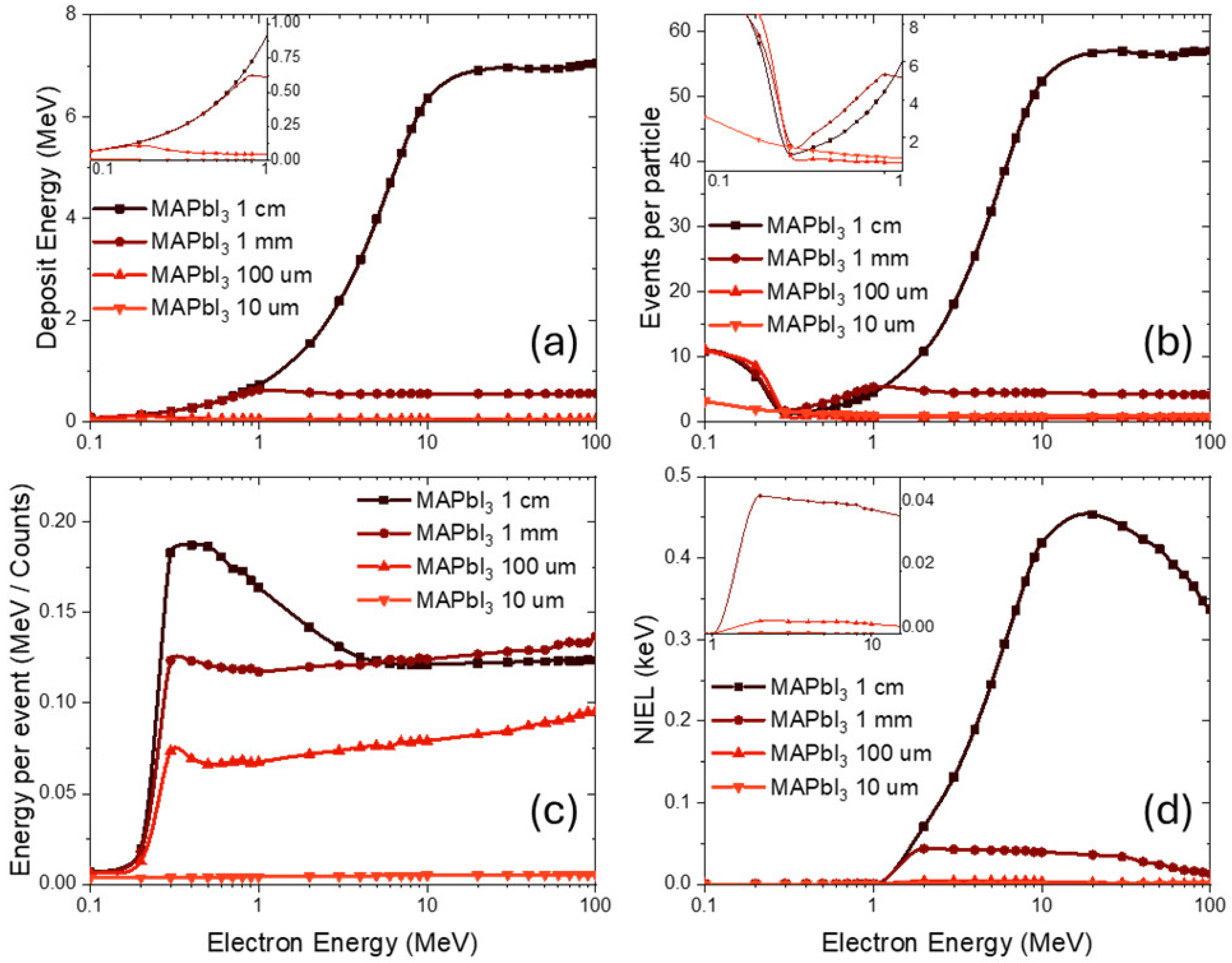
Let us now move on to a detailed examination of the influence of electrons of different energy ranges and the processes occurring in this case. The results of the Monte Carlo simulations are summarized in
Figure 3, which presents the dependence of deposit energy (
Figure 3a), the number of events per particle (
Figure 3b), the energy per event (
Figure 3c), and the non-ionizing energy loss—NIEL (
Figure 3d) in MAPbI
3 for absorber thicknesses of 1 cm, 1 mm, 100 µm, and 10 µm. As expected for electron irradiation in the 0.1–100 MeV energy range, the effective interaction volume decreases with decreasing absorber thickness. Consequently, the probability of radiation interacting with matter is reduced in thinner layers, leading to a pronounced drop in the absorbed fraction. For thick absorbers, the curves approach saturation, whereas for thin layers, most electrons traverse the material without significant interaction.
The number of events per particle (
Figure 3b) also tends to saturate, reflecting the reduced likelihood of multiple scattering when the material thickness is lowered. A small extremum appears at low energies around 0.1–0.3 MeV, which can be attributed to enhanced multiple Coulomb scattering at these energies, when scattering angles are large and many electrons undergo deflection events in rapid succession. As the energy increases, the scattering angles become smaller, multiple scattering is suppressed, and the curves converge to lower values [
44,
45].
The energy per event (
Figure 3c) exhibits the opposite trend: at very low energies, the deposited energy per interaction is small while the number of scattering events is large, which results in low energy per event. With increasing electron energy, the event frequency drops while the contribution of each interaction grows, leading to a broad maximum in the range of 0.2–0.7 MeV. Beyond this point, single scattering events and ionization dominate, followed by bremsstrahlung emission and the generation of secondary cascades. At still higher energies, electrons traverse the material more freely, and the average deposited energy per interaction decreases again.
The non-ionizing energy loss (
Figure 3d) follows a similar thickness-dependent trend, with saturation observed in bulk MAPbI
3 and more gradual increases in thinner absorbers. For thick targets, the curves rise until saturation is reached, since the interaction volume is sufficient to absorb a significant fraction of the incoming radiation before electrons start to pass through without interaction. In contrast, thin layers exhibit earlier saturation and lower overall values, as their limited volume makes it unlikely for an electron to undergo multiple collisions before escaping.
Taken together, these results confirm the expected scaling behavior: thicker perovskite layers provide a higher effective cross section for interaction, while thinner films are increasingly transparent to high-energy electrons. The observed maxima and saturation points reflect the transition between regimes dominated by multiple scattering at low energies, single-event ionization and bremsstrahlung at intermediate energies, and nearly unperturbed electron transmission at high energies.
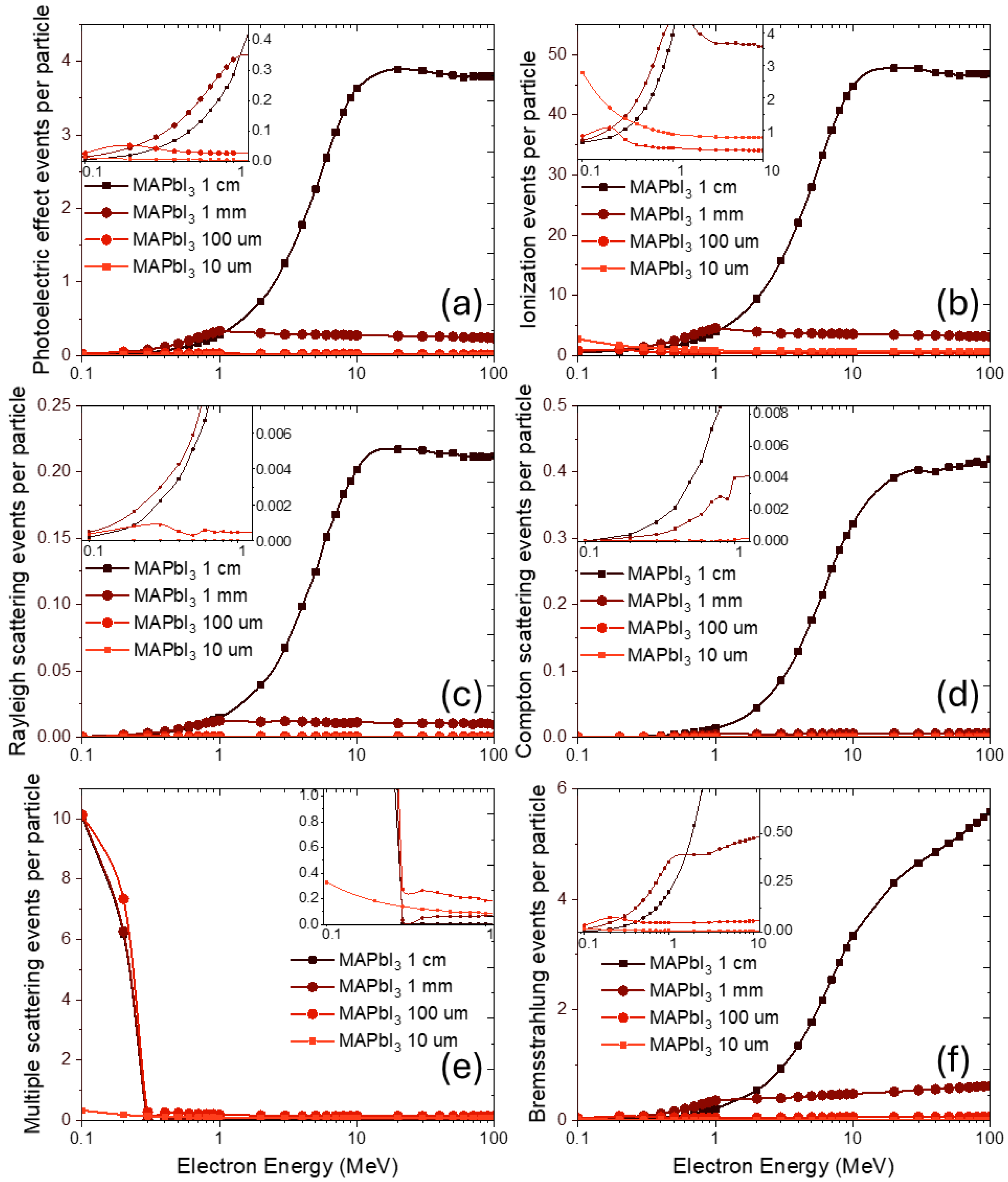
Figure 4 highlights the main physical processes underlying these observations. At low incident energies, multiple electron scattering (
Figure 4e) and ionization (
Figure 4b) dominate, giving rise to a high frequency of events per particle. This behavior is directly related to Coulomb scattering, where lower electron energies correspond to larger scattering angles and, therefore, more frequent deflection events. As the electron energy increases, scattering angles become smaller, leading to a reduction in multiple scattering. In this regime, the probability of single scattering events rises, and direct ionization becomes a major channel of energy deposition.
Alongside these primary processes, bremsstrahlung (
Figure 4f) emission and the generation of secondary particles, such as electrons and photons, play a progressively important role with increasing energy. The emitted photons can subsequently undergo photoelectric effect (
Figure 4a), Rayleigh scattering (
Figure 4c), or Compton scattering (
Figure 4d) within the perovskite lattice, further redistributing energy and contributing to defect generation.
The relative weight of these mechanisms shifts with energy: at lower energies, multiple scattering and direct ionization dominate, while at higher energies, bremsstrahlung and photon-induced secondary processes become more significant. For thick MAPbI3 layers, saturation is observed in most processes due to the large effective interaction volume. In contrast, thinner samples demonstrate earlier saturation and eventually a decline, since the limited thickness makes electron transmission more probable than interaction.
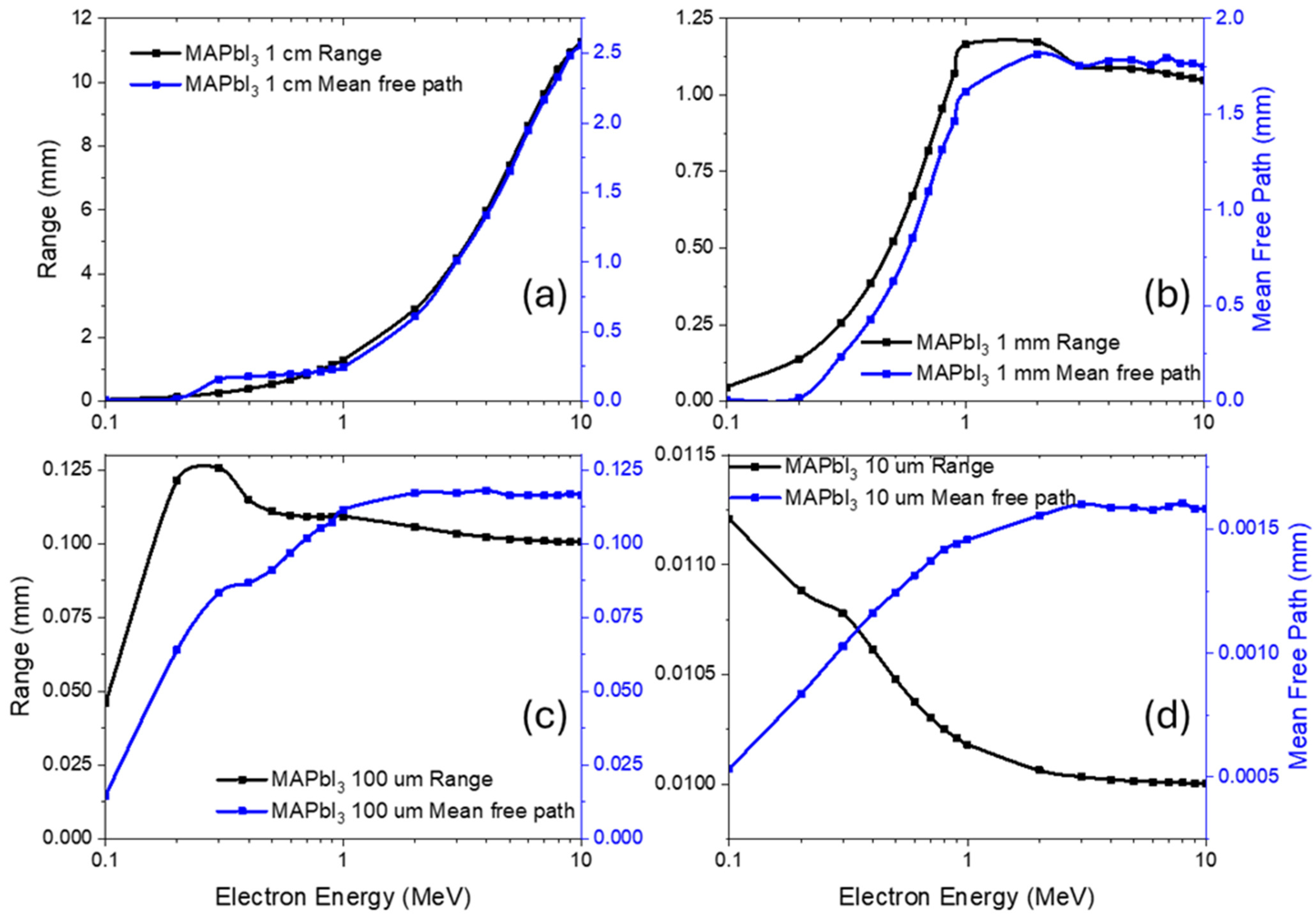
The energy dependence of these processes is further reflected in the data presented in
Figure 5, which shows the electron range and mean free path as functions of incident energy.
For MAPbI
3 layers on the centimeter scale (
Figure 5a), electrons with energies above several MeV are able to traverse the material completely, resulting in a steadily increasing penetration depth. In thinner absorbers (
Figure 5b–d), however, the effective electron range reaches saturation more rapidly, as electrons escape before experiencing a sufficient number of interactions. At intermediate energies, a broad maximum appears in the mean free path, reflecting the reduced scattering probability once the transition from multiple Coulomb scattering to single-event dominated transport occurs.
In the case of very thin layers (
Figure 5c,d), the majority of high-energy electrons pass through without interaction, and the mean free path reaches saturation at lower values compared to thicker targets. This behavior once again emphasizes the role of absorber thickness in defining the balance between energy deposition and transmission: while bulk MAPbI
3 can effectively sustain cascades of scattering and ionization events, thin layers quickly lose this capacity, becoming increasingly transparent to high-energy electrons.
The results of the Monte Carlo simulations provide important insight into how absorber thickness determines the balance between energy deposition and transmission in MAPbI3 under electron irradiation. For photovoltaic applications, where active layers are typically on the order of a few hundred nanometers, our findings suggest that such thin films will be largely transparent to high-energy electrons in the MeV range. In this regime, most particles traverse the material without interaction, and the absorbed dose is insufficient to produce significant bulk damage.
Nevertheless, localized ionization and defect formation can still occur, particularly through exciton generation and subsequent non-radiative relaxation pathways. These processes may contribute to ion migration, transient lattice disorder, or even radiolysis of the organic cation sublattice, ultimately impacting device stability under prolonged exposure.
For radiation detectors and dosimeters, however, thicker perovskite layers (tens to hundreds of micrometers) are more appropriate. At these thicknesses, the effective interaction volume is sufficient to sustain multiple scattering and ionization cascades, leading to stronger signals and enhanced sensitivity to incident electron fluxes. This explains why perovskite-based X-ray and electron detectors often employ films well above the typical photovoltaic thickness, ensuring both high stopping power and robust defect-mediated responses that can be correlated with dose. At even larger scales, such as millimeter to centimeter absorbers, saturation of deposited energy is observed, and the material can act as a bulk-like absorber suitable for high-flux dosimetry.
In terms of microscopic mechanisms, our results reinforce the idea that defect formation in hybrid halide perovskites is not governed by ballistic displacement, but rather by electronic excitation and ionization processes. The decay of high-density electron–hole populations can drive the formation of halide vacancies, most notably iodine vacancies, which are known to act as efficient non-radiative recombination centers.
At the same time, exciton formation and photoexcitation-induced carrier localization may in some cases transiently enhance photovoltaic performance, as observed in light-soaking effects. However, under sustained irradiation, the same processes promote the redistribution of ions within the lattice and the gradual build-up of irreversible degradation. In hybrid systems, radiolysis of the organic cations adds an additional instability pathway, leading to decomposition products that further accelerate device failure.
Taken together, these findings highlight the dual role of electron irradiation in MAPbI3: while thin films in photovoltaic geometries are relatively resistant to macroscopic damage due to their low interaction volume, the underlying electronic excitation channels still promote defect formation and ionic migration that compromise long-term stability. For detector and dosimetry applications, thicker films offer higher sensitivity and effective energy deposition, but at the cost of increased susceptibility to defect accumulation and irreversible degradation. This trade-off underscores the importance of carefully tailoring perovskite thickness and composition for specific radiation environments.
