Abstract
Silicon nanowire networks (nanonets) is an emerging candidate technology for sensor applications. In this work, we characterized Field Effect Transistor (FETs) employing silicon nanonet channels and evaluated their performance as photodiodes. We found that shorter and higher density nanonet channels have lower resistance and higher current flow. The drain current of the FETs doubled when irradiated with a continuous wave He-Ne laser (wavelength 632 nm). Finally, we examined the long-term stability of the FETs. The channel resistance increased by one order-of-magnitude after 6 months of storage in open air.
1. Introduction
Silicon nanowires (SiNWs) are one of the most widely studied nanostructures [1] deployed into many applications, such as biosensors [2], solar cells [3] and batteries [4]. In addition to interesting electrical and mechanical properties, they also have a high aspect ratio which makes them suitable for sensor applications. However, fabricating SiNWs with repeatable characteristics has proven challenging [5].
It was found that a more affordable and less complex approach is to produce networks of randomly distributed SiNWs, dubbed “nanonets” [6], with repeatable characteristics. These nanonets have, on average, similar mechanical, chemical and electronic properties. Recent years have seen increasing interest in nanonets. While interests has focused on carbon [6] and metallic nanonets [7], silicon nanonets have been recently fabricated and proposed as biosensor applications [8].
In this work; we characterize silicon nanonet-based field effect transistors (FETs) and explore their use as photodiodes. First, we compare the channel resistance among nanonet FETs with three different densities: Low (5.9 × 10⁷ SiNWs/cm2), medium (8.2 × 10⁷ SiNWs/cm2), and high (10.4 × 10⁷ SiNWs/cm2). Second, we compare channel resistance for nanonet channel gaps of 5 µm, 15 µm and 30 µm. Third, we evaluate the nanonet FETs performance as photodiodes. Finally, we examine the long-term stability of the nanonet FETs.
2. Methods
2.1. FET Fabrication
Silicon nanowires, average diameter 40 nm and length 7 μm, were synthesized as detailed previously [8,9]. After growth, SiNWs were dispersed by sonication into deionized water for 5 min. Three different volumes of this suspension (24 mL, 34 mL and 46 mL) were vacuum-filtered through a nitrocellulose membrane forming nanonets with density of 5.9 × 10⁷, 8.2 × 10⁷ and 10.4 × 10⁷ NWs/cm2, respectively. To fabricate the transistors, the nanonets were transferred onto 200 nm-thick Si3N4 layer on top of a heavily doped silicon substrate by filter dissolution. Figure 1 displays a schematic of the fabricated device. SEM images were used to verify the homogeneity of the nanonet on the Si/Si3N4 substrate, thereby ensuring successful transfer.
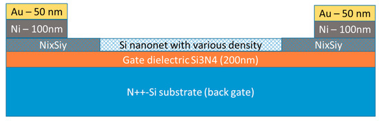
Figure 1.
Cross-Section of Si Nanonet FET.
After the transfer, the nanonet conductivity is enhanced through sintering to create conducting paths at NW/NW junctions [9]. With this aim, rapid thermal annealing was carried out on the nanonets under nitrogen at 400 °C for 1 min. The source and drain contacts are defined by photolithography and lift-off of a stack consisting of 100-nm-thick nickel and 50-nm-thick gold. Good contact between the semiconductor and electrodes is achieved through the silicidation performed at 400 °C for 1 min.
2.2. FET Characterization
In order to compare the channel resistance of the silicon nanonet FETs, their I-V curves were obtained using two Keithley 2400 SMUs. One SMU was used to supply gate voltage. Another SMU equipped with tungsten tips supplied the drain voltage and measured the drain current (Figure 2). The source was grounded. A laptop controlled and synchronized the two SMUs through serial ports and recorded their measurements. The gate voltage was swept up and down in the range Vgs = −25 − 25 V in steps of 1 V, while the drain voltage remained constant.
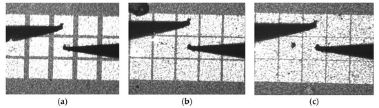
Figure 2.
Pictures of (a) 30 µm; (b) 15 µm; and (c) 5 µm channel gap Si nanonet FETs.
3. Results and Discussion
3.1. Characterization of the Si nanonet FETs
We plot the drain current-gate voltage curves for low, medium and high-density Si nanonet FETs in Figure 3 at a drain voltage of Vds = −4 V. Each subfigure shows the curves for two consecutive gate voltage up-down sweeps for FETs with 5 µm, 15 µm and 30 µm channel, where channel gap is defined as the distance between source and drain contacts. Up sweeps are shown in solid lines and down sweeps are shown in dashed lines. Comparing the three subfigures, we found that the drain current for high density nanonet FETs (10.4 × 10⁷ SiNWs/cm2) is similar to that for medium density nanonet FETs (8.2 × 10⁷ SiNWs/cm2) and that both are significantly higher than that for low density nanonet FETs (5.9 × 10⁷ SiNWs/cm2). We conclude that higher density nanonets have lower channel resistance than low density nanonets due to the formation of more conducting paths linking the source and the drain.
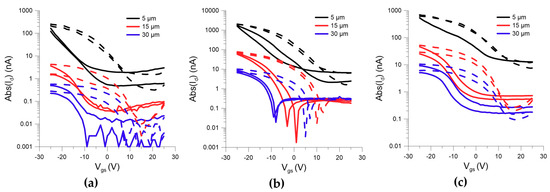
Figure 3.
The Id-Vgs curves for (a) low density; (b) medium density and (c) high density Si nanonet FETs under and gate voltage up (solid lines) and down (dashed lines) sweeps and a drain voltage of Vds = −4 V.
Irrespective of the channel density, we found that the drain current for the 30 µm channel nanonet FETs was lower than the drain current for the 15 µm channel nanonet FETs, which in turn is lower than the drain current for 5 µm channel nanonet FETs. In fact, the drain current for the low density 30 µm channel nanonet FETs was below the noise floor for gate voltages higher than Vds = −10 V. This indicates that FETs with shorter gaps have lower channel resistance than those with longer gaps. The variability in the nanonet FETs characteristics under consecutive voltage sweeps indicates the presence of hysteretic effects in the channel conductance. This hysteresis is considerable extending over several volts. This phenomenon is characteristic of a trapping-detrapping mechanism that takes place at the interface between the native oxide and the NW surface. By taking into account the sweep rate, 1 V/s, we can deduce that these traps interact slowly with the interface.
3.2. Evalutation of the Si Nanonet FETs as Photodiodes
We used a continuous wave He-Ne laser (power <1 mW, wavelength 632 nm) to irradiate the high density, 5 µm long nanonet channel FETs and measured the drain current while the gate voltage was swept up and down. In Figure 4, we compare the drain current-gate voltage curves when the laser was turned on and off at drain voltages of Vds = 1 V and Vds = 5 V. Up sweeps are shown in solid lines and down sweeps are shown in dashed lines. We found that laser irradiation almost doubled the drain current throughout the operation range. For example, during gate voltage up sweeps maximum drain current (at Vgs = −25 V) increased from Id = 52 nA to 128 nA for Vds = 1 V and from Id = 323 nA to 643 nA for Vds = 5 V. Similarly, during gate voltage down sweeps drain current (at Vgs = −25 V) increased from Id = 73 nA to 156 nA for Vds = 1 V and from Id = 337 nA to 762 nA for Vds = 5 V. The doubling in the drain voltage current allows us to conclude that Si nanonet FETs are viable candidates as photodiodes.
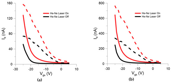
Figure 4.
The Id-Vgs curves of the high density Si nanonet FETs when irradiation with He-Ne Laser was set on and off under gate voltage up (solid lines) and down (dashed lines) sweeps and a drain voltage of (a) Vds = 1 V and (b) Vds = 5 V.
3.3. Long Term Stability of the Si Nanonet FETs
In pursuance of understanding the long-term stability of Si nanonet FETs, we measured the drain current-gate voltage curves for medium density 5 µm and 15 µm nanonet channel FETs in March 2017 and the same curves for those FETs in September 2017, after 6 months of storage in open air. The Id-Vgs curves before and after aging are compared in Figure 5 for medium density nanonet FETs and in Figure 6 for high density nanonet FETs under gate voltage up sweeps. First, we note that increasing drain voltage increases the drain current as expected. The results also show one order-of-magnitude drop in drain current for both medium and high density nanonet FETs.
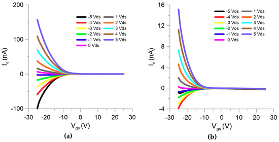
Figure 5.
The up-sweep Id-Vgs curves for medium density 15 µm nanonet channel FETs measured in (a) March and (b) September 2017.
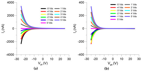
Figure 6.
The up-sweep Id-Vgs curves for medium density 5 µm nanonet channel FETs measured in (a) March and (b) September 2017.
Since the nanonets were treated to prevent NW-NW junction oxidation [9], such a decrease in conductance is not due to appearance of a barrier at the junctions. As a consequence, we surmise that the sweep-on-sweep variability in conductance, observed above, and the degradation in conductance over time, observed here, are due to charge trapping in the nanonet channels and at NW/oxide interface as well as interaction with environment since the FETs behavior is highly sensitive to surface modification.
4. Conclusions
We characterized the channel resistance of Si nanonet FETs with varying nanonet densities and channel gaps and found that shorter and higher density channels have lower resistance and higher currents. We also evaluated Si nanonet FETs potential for use as photodiodes by measuring the drain current while continuous wave He-Ne laser (wavelength of 632 nm) irradiation was turned on and off. The drain current almost doubled due to laser irradiation irrespective of the drain and gate voltages. Although further work is required to optimize the FETs performances and their sensitivity to light, the present results indicate that they are good candidates for miniaturized photodiodes. Finally, we examined the long-term stability of silicon nanonet FETs and found that channel resistance increased by an order-of-magnitude after six months of storage in open air. Further work is required to examine the underlying causes of charge trapping in the channels and increase in their resistance overtime and to devise methods to overcome these challenges.
Author Contributions
C.T., M.L. and B.S. fabricated the Si nanonet FETs. S.P. and M.I. designed the experiments, while M.K. and S.P. carried them out. M.K. wrote the initial draft of the manuscript and E.A.-R., C.T. and M.L. revised it. C.T., E.A.-R. and M.Y. supervised the research effort and reviewed the final manuscript.
Acknowledgments
The authors would like to acknowledge the support of the Canadian Microelectronics Corporation. This work has received funding from the EU H2020 RIA project Nanonets2Sense under grant agreement No. 688329.
Conflicts of Interest
The authors declare no conflict of interest.
References
- Dasgupta, N.P.; Sun, J.; Liu, C.; Brittman, S.; Andrews, S.C.; Lim, J.; Gao, H.; Yan, R.; Yang, P. Semiconductor nanowires—Synthesis, characterization, and applications. Adv. Mater. 2014, 26, 2137–2184. [Google Scholar] [CrossRef] [PubMed]
- Zhang, G.; Ning, Y. Silicon nanowire biosensor and its applications in disease diagnostics: A review. Anal. Chim. Acta 2012, 749, 1–15. [Google Scholar] [CrossRef] [PubMed]
- Garnett, E.; Yang, P. Light trapping in silicon nanowire solar cells. Nano Lett. 2010, 10, 1082–1087. [Google Scholar] [CrossRef] [PubMed]
- Chan, C.K.; Peng, H.; Liu, G.; McIlwrath, K.; Zhang, X.F.; Huggins, R.A.; Cui, Y. High-performance lithium battery anodes using silicon nanowires. Nat. Nanotechnol. 2008, 3, 31–35. [Google Scholar] [CrossRef] [PubMed]
- Serre, P.; Mongillo, M.; Periwal, P.; Baron, T.; Ternon, C. Percolating silicon nanowire networks with highly reproducible electrical properties. Nanotechnology 2015. [Google Scholar] [CrossRef] [PubMed]
- Gruner, G. Carbon nanotube films for transparent and plastic electronics. J. Mater. Chem. 2006, 16, 3533–3539. [Google Scholar] [CrossRef]
- Dong, Q.; Zafir, M.; Nasira, M.; Pumera, M. Semi-conducting single-walled carbon nanotubes are detrimental when compared to metallic single-walled carbon nanotubes for electrochemical applications. Phys. Chem. Chem. Phys. 2017, 19, 27320–27325. [Google Scholar] [CrossRef] [PubMed]
- Legallais, M.; Nguyen, T.T.T.; Mouis, M.; Salem, B.; Robin, E.; Chenevier, P.; Ternon, C. An innovative large scale integration of silicon nanowire-based field effect transistors. Solid-State Electron. 2017; in press. [Google Scholar]
- Ternon, C.; Serre, P.; Lebrun, J.; Brouzet, V.; Legallais, M.; David, S.; Luciani, T.; Pascal, C.; Baron, T.; Missiaen, J. Low temperature processing to form oxidation insensitive electrical contact at silicon nanowire/nanowire junctions. Adv. Electron. Mater. 2015. [Google Scholar] [CrossRef]
Publisher’s Note: MDPI stays neutral with regard to jurisdictional claims in published maps and institutional affiliations. |
© 2018 by the authors. Licensee MDPI, Basel, Switzerland. This article is an open access article distributed under the terms and conditions of the Creative Commons Attribution (CC BY) license (https://creativecommons.org/licenses/by/4.0/).