Proceeding Paper

Optimized Batch Process for Organic MEMS Devices †

Institute of Sensor and Actuator Systems, TU Wien, 1040 Wien, Austria
*
Author to whom correspondence should be addressed.
Presented at the Eurosensors 2018 Conference, Graz, Austria, 9–12 September 2018.
Proceedings 2018, 2(13), 904; https://doi.org/10.3390/proceedings2130904
Published: 28 November 2018
(This article belongs to the Proceedings of EUROSENSORS 2018)

Abstract

:
Recently, organic electromechanical transducers have attracted intense scientific and technological interest due to their unique mechanical flexibility and their piezoelectric properties. However, the fabrication of organic MEMS devices is challenging. For example, a lift-off process cannot be used on polymers, because of the solvent in photoresists. Here, we present a straightforward and low-cost batch process for organic MEMS devices using standard micromachining techniques. As organic material we used the ferroelectric (co-)polymer poly(vinylidene fluoride-trifluorethylene) (P(VDF-TrFE)). The integration of the polymer in a CMOS-compatible process was optimized in terms of deposition and patterning of the polymer and the corresponding metal layers. Micromachined devices, such as capacitors and cantilevers, were fabricated and analysed. The ferroelectric perfomance was evaluated by electrical and electromechanical measurements. Our first results indicate that the proposed fabrication process is reliable resulting in well-functioning organic MEMS devices. We measured as piezoelectric constant a d33 of −32 pm/V with our organic P(VDF-TrFE) capacitors.

1. Introduction

The number of different piezoelectric materials used in micromachined sensors, actuators and energy harvesters is quite large [1,2,3,4]. The most common used materials are ceramics like lead zirconate-titanate (PZT) or aluminium nitride (AlN). Recently, piezoelectric organic materials gain increasing importance in MEMS devices, especially in the field of flexible and soft electronics. Due to the low-cost and their remarkable electromechanical properties, organic MEMS have the potential to enlarge or even replace standard sensor and actuator solutions made of inorganic MEMS. However, the integration of functional organic materials in a standard microfabrication process is challenging, because typical chemicals, such as the solvent acetone, attack or even destroy most of the polymers. To overcome these problems and to exploit the full potential of this material class for MEMS/NEMS devices, we present a simple and low-cost batch process.
Within the most well known electroactive polymers falls the class of fluoropolymers with poly(vinylidene fluoride) (P(VDF)) and its copolymers, such as poly(vinylidene fluoride70-trifluorethylene30) (P(VDF70-TrFE30)). This family of functional materials is characterized by its unique ferroelectric and piezoelectric properties. P(VDF70-TrFE30) has a piezoelectric constant d33 of around −32 pm/V and is therefore significantly above the piezoelectric constant of, e.g., AlN with a d33 of only 4–6 pm/V [3,4]. In addition, the mechanical flexibility of the polymer P(VDF70-TrFE30) with a Young’s Modulus of 2 GPa is superior to that of ceramics, such as AlN with a value of 310 GPa [5]. Thus, electroactive polymers are predestined for energy harvesters [1]. Further characteristic material parameters of P(VDF70-TrFE30) are presented in Table 1.
There are several approaches for the fabrication of organic MEMS devices in literature [6,7,8]. However, some process steps lead to problems. For example, in most cases the electrode is patterned on the polymer by a lift-off process [6,7]. Or the design of the bottom- and top-electrode to each other is not considered [6,7,8]. These errors will be explained and solved in more detail here. By tailored process steps, it is possible to fabricate organic MEMS devices in a CMOS-compatible process flow.

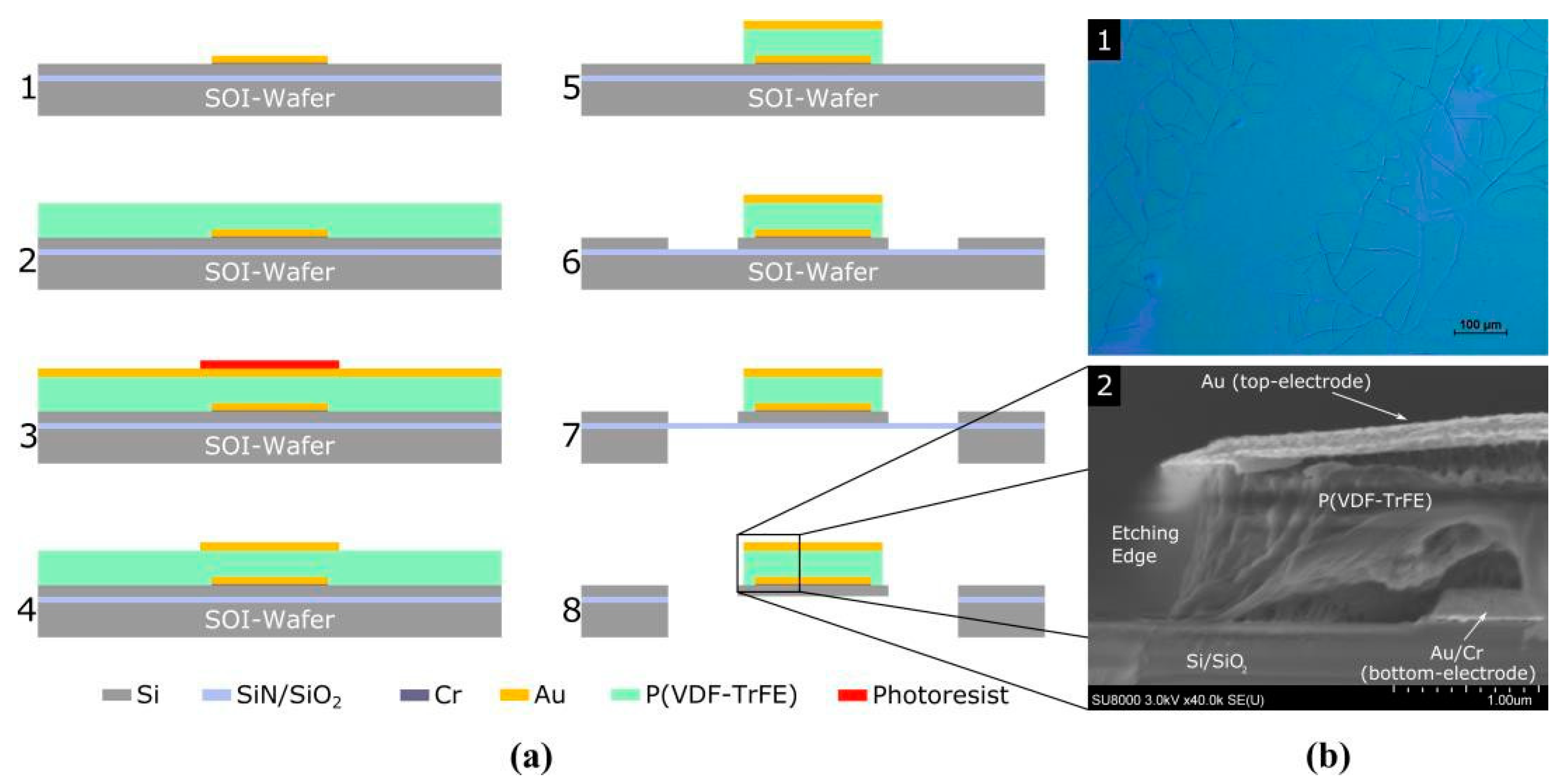
2. Fabrication Process

In the following, we present a process flow for the fabrication of organic MEMS devices. We focus on the realization of a cantilever-type MEMS device with the polymer P(VDF70-TrFE30) as electromechanical transducer. The most important process steps used to fabricate the cantilevers are presented in Figure 1a. In order to investigate the electroactive performance of the polymer thin films, standard capacitors were fabricated in parallel.
In the first step, we start with a 4″ silicon on insulator (SOI) wafer coated with silicon-rich LPCVD silicon nitrid (SiN) and PECVD silicon dioxide (SiO2). Then, the bottom electrodes were formed by a conventional lift-off process. For this purpose, 50 nm of chromium (Cr) was deposited by electron-beam evaporation as an adhesion promoter for a 200 nm gold (Au) layer to increase the electrical conductivity of the bi-layered metallization. Subsequently, a 1 µm thin polymer film was spin-coated at 3000 rpm from solutions of P(VDF70-TrFE30) powder in methyl ethyl ketone (MEK). The polymer powder was purchased from Piezotech/Arkema Group. The weight ratio of P(VDF70-TrFE30) and MEK in the solutions were 8%. For a slow evaporation of the solvent, the polymer film was kept for 10 min at 80 °C being the evaporation temperature of MEK. Followed by an annealing process at 130 °C for 2 h in a vacuum oven to increase the crystallinity of the material. To form the top electrodes, 200 nm Au was evaporated over the entire surface of the polymer and patterned by a wet-chemical etching process. An adhesion promoter was not necessary, since the adhesion between Au and P(VDF70-TrFE30) was sufficient. In literature lift-off processes are commonly used to pattern the top electrodes [7,8]. However, standard solvents for photoresists, such as propylene glycol monomethyl acetate (PGMEA), attack the polymer such, that large cracks result all over the polymer layer (see Figure 1b). Therefore a wet chemical etching process was developed to protect the polymer by the Au layer. Another critical step is the anisotropic etching of the polymer. To ensure low underetching and steep edge characteristics a reactive ion etching (RIE) process with 50 sccm O2 gas flow, 150 mTorr chamber pressure and a plasma power of 150 W was used, whereas the top electrode serves as hard mask for the etching process. Furthermore, the top electrode must be designed larger than the bottom electrode. This minimize any electrical short cut between the top and the bottom electrode if underetching occurs. A SEM image of the cut through an organic cantilever is shown in Figure 1b. It can be clearly seen that the top electrode is about 1 µm larger than the bottom electrode. In addition, the image shows that the chosen etching parameters provide low underetching and steep etching edges. The polymer film was poled only once after the fabrication with an electric field of 100 V/µm by applying a DC voltage.

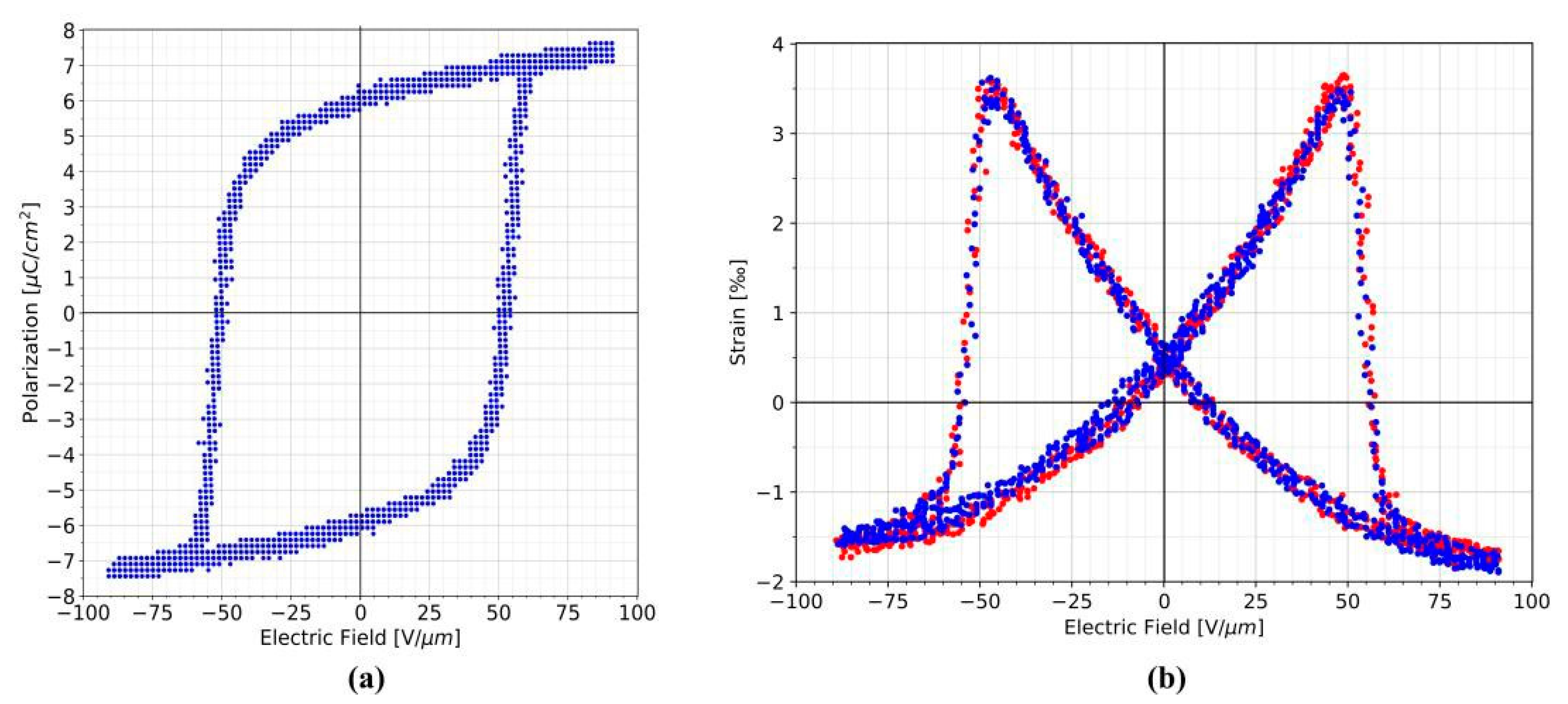
3. Results and Discussion

In order to study the functionality of the organic MEMS devices, we measured their piezoelectric perfomance, thus focusing on the ferroelectric properties of the thin polymer films. For this purpose, the electrical and electromechanical properties of the organic material P(VDF70-TrFE30) were determined.
For the electrical characterization the relative permittivity εr was measured using micromachined fabricated capacitors having different electrode areas. A linear fit curve was used to extract the unit area capacitance in order to minimize the error due to parasitic capacitances arising from the setup. We obtained a relative permittivity εr = 14 of P(VDF70-TrFE30) at room temperature and at 1 kHz, respectively. In addition, the electric polarization (P) was measured as a function of the applied electric field (E) via a Sawyer-Tower bridge. The resulting P-E hysteresis is presented in Figure 2a. Higher remanent polarization (Pr) implies stronger piezoelectric response and the coercive field (Ec) indicates the required poling conditions. We obtained a remanent polarization of 6.2 µC/cm2 and a coercive field of ±50 V/µm. Basically, our organic P(VDF70-TrFE30) capacitors show the typical characteristics of this polymer. The hysteresis remained unchanged over several cycles up to 104 at 10 Hz.
The electromechanical behaviour of the polymer films was determined by AFM measurements. For this purpose, a silicon nitride cantilever was placed on the top electrode of a capacitor. To measure the piezoelectric displacement, an AC signal was applied. The vertical displacement of the polymer deflects the probe and hence the strain (S) is measured as a function of the electric field. The resulting S-E butterfly curve is shown in Figure 2b. The capacitor was attached to the sample holder by vacuum, so that clamping effects did not occur. To calculate the piezoelectric constant, we used the relation
d 33 = S E | E = 0
and we obtained a piezoelectric constant d33 = −32 pm/V for P(VDF70-TrFE30). Besides that, the coercive field of ±50 V/µm of the material can be clearly recognized here as well.
Both electrical and electromechanical measurements demonstrate that even after several cycles up to 104 at 10 Hz the organic MEMS devices exhibit a stable piezoelectric activity, giving confident in our device technology.

4. Conclusions

We have presented a straightforward and low-cost batch process for organic MEMS devices. The resulting electroactive performance has been evaluated demonstrating excellent piezoelectric performance. We have identified and solved the challenges in the fabrication of organic MEMS devices. For P(VDF70-TrFE30), we measured a piezoelectric constant of −32 pm/V with our organic capacitors. The P-E hysteresis and S-E butterfly curve remained stable at room temperature even after 104 cycles at 10 Hz.

Acknowledgments

This work has received funding from the European Union’s Horizon 2020 research and Innovation programme under the Marie Sklodowska-Curie grant agreement No. 721874 (SPM2.0).

References

  1. Torah, R.; Lawrie-Ashton, J.; Li, Y.; Arumugam, S.; Sodano, H.; Beeby, S. Energy-harvesting materials for smart fabrics and textiles. MRS Bull. 2018, 43, 214–219. [Google Scholar] [CrossRef]
  2. Gautschi, G. Piezoelectric Materials for Sensors. In Piezoelectric Sensorics; Springer: Berlin/Heidelberg, Germany, 2002; pp. 13–50. [Google Scholar]
  3. Ababneh, A.; Schmid, U.; Hernando, J.; Sánchez-Rojas, J.L.; Seidel, H. The influence of sputter deposition parameters on piezoelectric and mechanical properties of AlN thin films. Mater. Sci. Eng. B 2010, 172, 253–258. [Google Scholar] [CrossRef]
  4. Schneider, M.; Bittner, A.; Schmid, U. Improved Piezoelectric Constants of Sputtered Aluminium Nitride Thin Films by Pre-conditioning of the Silicon Surface. J. Phys. D Appl. Phys. 2015, 48, 405301. [Google Scholar] [CrossRef]
  5. Bruls, R.J.; Hintzen, H.T.; de With, G.; Metselaar, R. The temperature dependence of the Young’s modulus of MgSiN2, AlN and Si3N4. J. Eur. Ceram. Sci. 2001, 21, 263–268. [Google Scholar] [CrossRef]
  6. Yildirim, Y.A.; Toprak, A.; Tigli, O. Piezoelectric Membrane Actuators for Micropump Applications Using PVDF-TrFE. J. Microelectromechan. Syst. 2018, 27, 86–94. [Google Scholar] [CrossRef]
  7. Oh, S.R.; Yao, K.; Tay, F.E.H. Fabrication of piezoelectric P(VDF-TrFE) microcantilevers by wafer-level surface micromachining. J. Micromechan. Microeng. 2013, 23, 095023. [Google Scholar] [CrossRef]
  8. Toprak, A.; Tigli, O. MEMS Scale PVDF-TrFE-Based Piezoelectric Energy Harvesters. J. Microelectromechan. Syst. 2015, 24, 1989–1997. [Google Scholar] [CrossRef]
Figure 1. Fabrication of organic MEMS devices: (a) Process flow of P(VDF-TrFE) based cantilevers: (1) Bottom electrode patterning (lift-off process), (2) Spin coating of P(VDF-TrFE), (3–4) Top electrode patterning (wet chemical etching), (5) O2-etching of P(VDF-TrFE), (6–8) Frontside and backside deep reactive-ion etching and HF-release; (b) (1) Large cracks all over the P(VDF-TrFE) layer after a lift-off process caused by the solvent PGMEA of the photoresist, (2) SEM image of the cut through an organic cantilever.
Proceedings 02 00904 g001
Figure 2. Ferroelectric performance of the polymer P(VDF70-TrFE30) at room temperature and at 10 Hz: (a) Polarization as a function of applied electric field measured with a Sawyer-Tower bridge (P-E hysteresis, ); (b) Strain as a function of applied electric field measured with an AFM (S-E butterfly curve, measurement 1, measurement 2).
Proceedings 02 00904 g002
Table 1. Characterisitic material parameters of the ferroelectric polymer P(VDF70-TrFE30).
Young’s Modulus Y2 GPa
Relative Permittivity εr14
Remanent Polarization Pr6.2 µC/cm2
Coercive Field Ec±50 V/µm
Piezoelectric Coefficient d33−32 pm/V
Publisher’s Note: MDPI stays neutral with regard to jurisdictional claims in published maps and institutional affiliations.

