1. Introduction
Thermal properties of materials are important in many microelectronics elements, automotive and even space applications, building industry, bioengineering and many other areas. Thermal conductivity, one of the key thermal characteristics, can be evaluated by several steady state and transient measurement techniques [
1]. One of the transient techniques is the 3-omega (3ω) method, best suitable for fast characterization of small solid samples [
2,
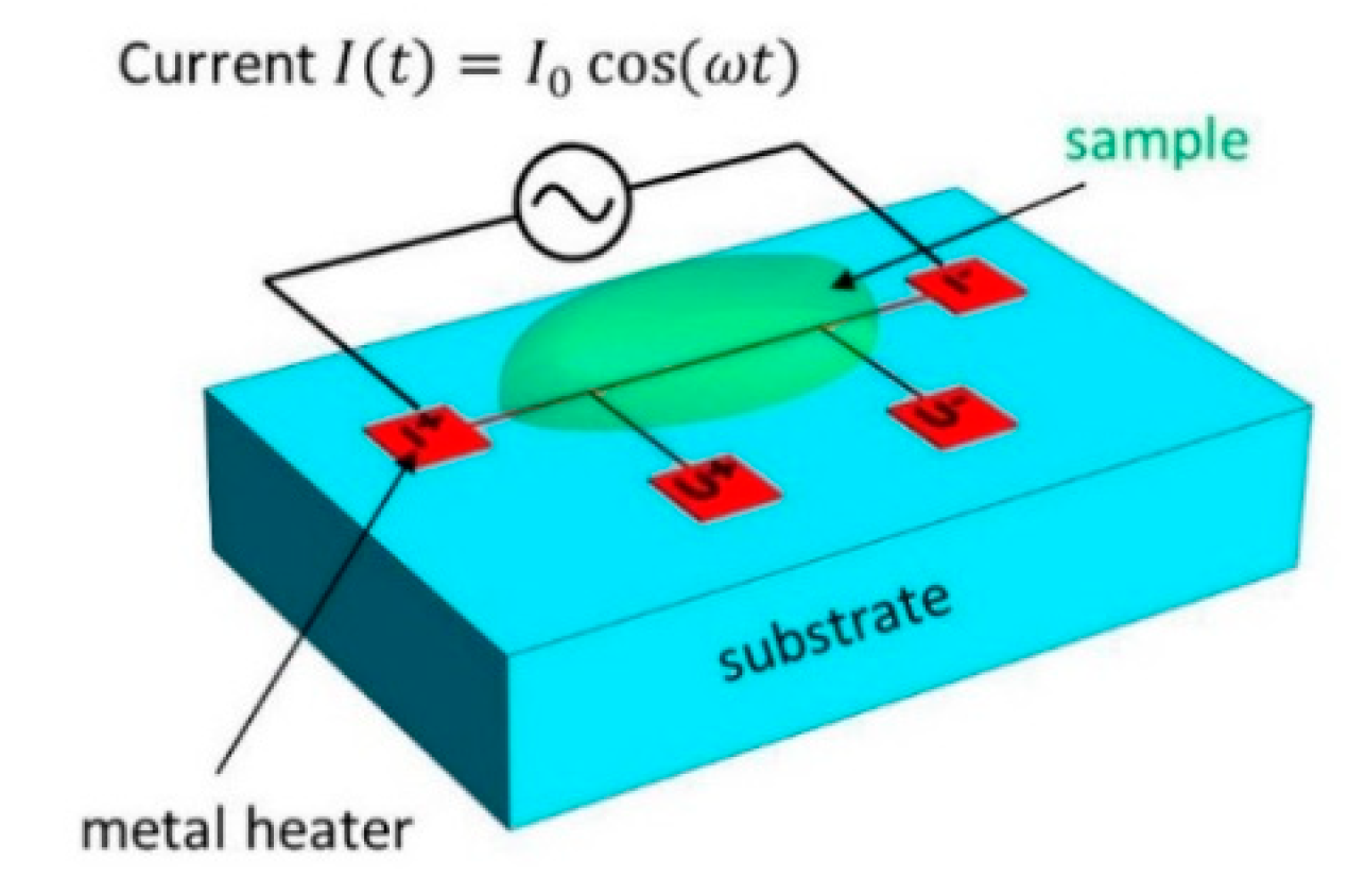
3]. Using the extension of the 3ω method allows for measurements of the thermal conductivity of liquid and solid samples. It can be realized by using a measurement chip in which the 3ω sensor is already integrated and the sample is deposited on top of the chip (
Figure 1) [
4,
5]. The microheater prepared on the chip acts as a sensor [
4,
5,
6]: the applied alternating current (of frequency ω) causes the heating of the sample (proportional to 2ω) what results in an additional voltage signal on the heater/sensor at the 3ω frequency. This signal depends on the thermal conductivity of the sample material. To minimize the influence of the measurement chip, the heater/sensor must be fabricated on material with low thermal conductivity.
In this work, 3ω measurement chips of different design have been fabricated on silicon and on glass. These materials were selected because of their low thermal conductivities. Several solid and liquid samples were characterized to demonstrate the performance of the devices.
2. Materials and Methods
2.1. Chip Fabrication
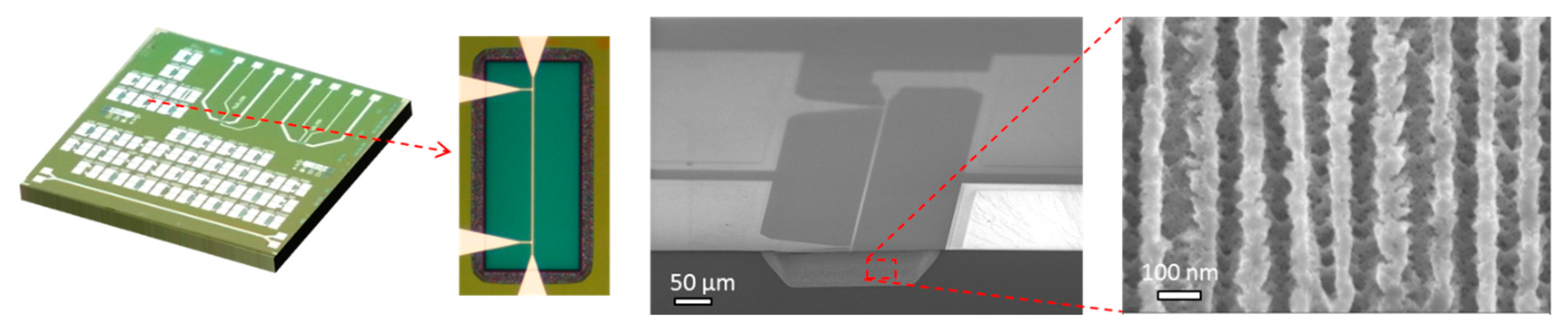
Both silicon (Si) and glass chips were fabricated on 150 mm diameter wafers using VTT’s cleanroom facilities. In the case of silicon, n-type wafers of 10–20 mOhm-cm resistivity were used. A silicon nitride layer was deposited and patterned by photolithography. This layer acted as a mask during the porous silicon (PS) formation by electrochemical etching in HF:ethanol = 1:1 containing electrolyte. 4 min etching at 300 mA/cm2 current density resulted in 50 µm deep PS wells with the average pore diameter of about 60–80 nm. The PS layer at the surface was rather smooth, with the pore diameter of only about 10–20 nm, what simplified the subsequent microfabrication steps. After porosification, 200 nm thick amorphous silicon oxide layer was deposited by plasma enhanced chemical vapour deposition (PECVD) technique and 80 nm of aluminum was sputtered and patterned to form the heater/sensors of different length and width. Then, a 300 nm thick Al layer was sputtered and patterned to form the contact pads for current and voltage terminals. PECVD oxide formed the electrical isolation for the Al-heater. Finally, the wafer was diced into 1 × 1 cm2 chips.
Figure 2 shows the chip and a photograph of one of the sensors on the Si/PS chip and scanning electron micrographs (SEMs) of the porous silicon layer under it.
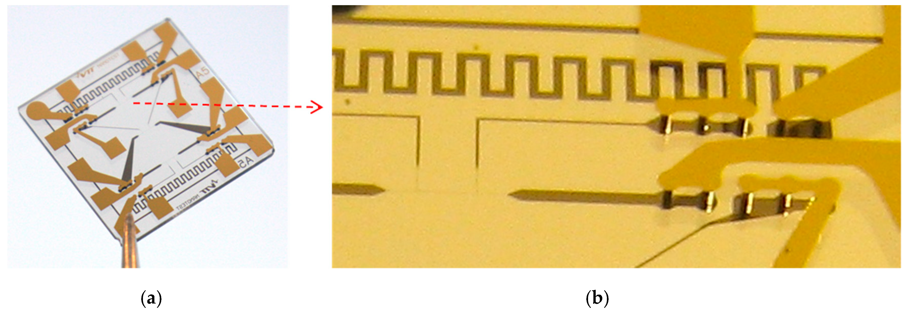
Glass chips for 3ω measurements were fabricated from Schott HermeS substrates with built-in through glass vias (TGVs). This allows preparation the heater/sensor and the contacts on the opposite sides of the chip and contacting them through tungsten filled TGVs (
Figure 3). The microfabrication of Al heaters/sensors on the top side was the same as for the silicon chips, as described earlier. The contact pads on the back side of the TGV wafers were done by sputtering and photolithographically patterning a 500 nm thick gold layer. After the cleaning steps, the top side was coated by atomic layer deposition (ALD) technique with an about 56 nm thick passivation layer. This layer was an (Al2O3/TiO2)x2 nanolaminate with about 14 nm thickness of each layer. Titanium oxide was added to improve the chemical resistance of the electrically isolating aluminum oxide layer. The last step was dicing into separate chips of 1.2 × 1.2 cm2. Each chip contains three heater/sensors and two additional meander type heaters (
Figure 3). More details on the glass chips can be found elsewhere [
5].
2.2. Measurement Procedure
For the 3ω measurement, the heater/sensor on the chip was connected in series with a series resistor (for current measurement) and a potentiometer, adjusted to the same electric resistance as the sensor. This allowed use of the common-mode-subtraction (CMS) which removes the 3ω signals not originating from the 3ω sensor [
5]. Voltage signals from sensor and from potentiometer were handled by a custom LabView software that performs the lock-in detection.
The slope of temperature dependence of the sensor resistor was determined from current voltage curves measured at different temperature keeping the chip in a heating chamber. The thermal conductivity
of the samples can be obtained using the slope method [
5]:
where
is the power,
L—length of the heater,
—the real part (in-phase component) of (Δ
T),
—the thermal conductivity of the substrate (evaluated by the same slope method by performing the measurement without a sample).
Good thermal contact between sample and heater/sensor is needed to keep the accuracy of the measurement. To satisfy this any voids or air gaps above and near the heater/sensor must be minimized. In the case of TGV glass chip, this can be easily controlled optically from the back side.
3. Results and Discussion
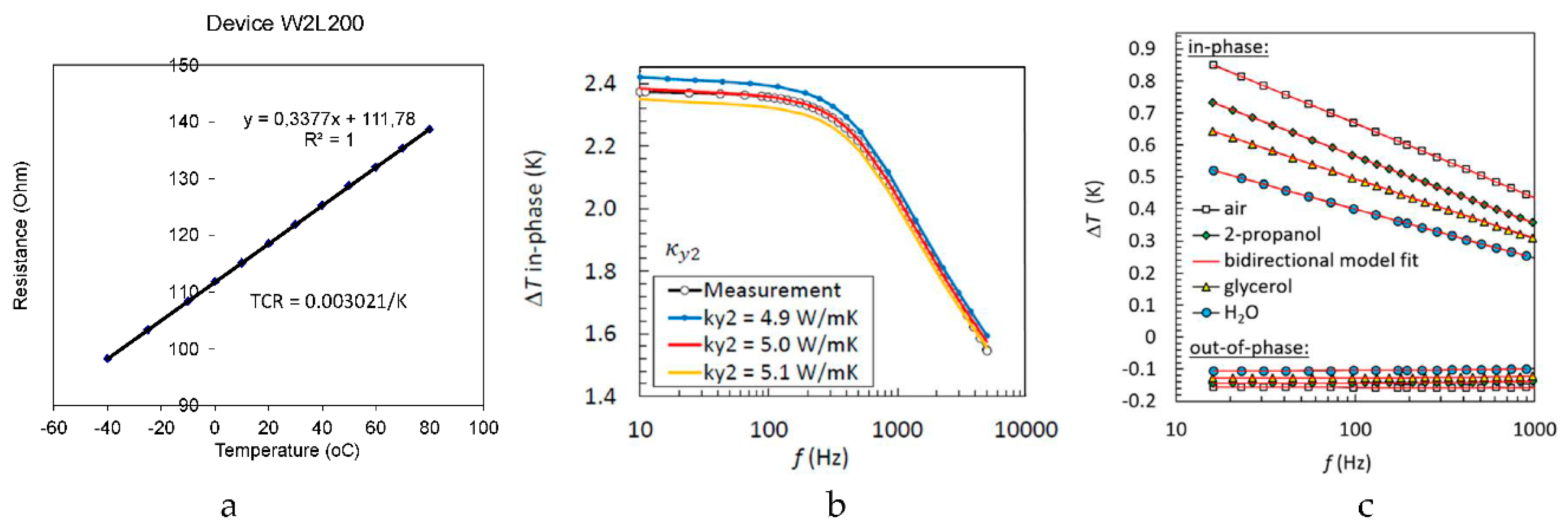
The chip characterization was done by evaluating the temperature coefficient of resistance (TCR) of the heater/sensor.
Figure 4a shows the measured temperature dependence of resistance for heater/sensor prepared on porous silicon layer. The evaluated TCR is 3.02 × 10
−3 K
−1. Almost the same value for TCR was obtained also for Al heater/sensor on TGV chip: 2.93 × 10
−3 K
−1.
3-omega measurement results are shown in
Figure 4b,c. Characterization of thermal properties of porous silicon layer under the heater/sensor was performed on Si/PS chip. By fitting experimental results with the modelling curves, the value of 3.8 W/mK was obtained (
Figure 4b). This is appropriate value for macroporous silicon. Multilayer model was used for the fitting, including silicon substrate, PS layer and the passivating silicon oxide. The curves in the semi-logarithmical scale are not linear, most probably due to complex structure and due to not uniform structure of porous silicon (pores at the surface are almost order of magnitude smaller). This makes characterization of thermal conductivity of the sample on top of PS layer more complicated. Most probably, oxidized PS with lower thermal conductivity could reduce influence of the substrate and the oxide layer.
The determination of the sample thermal conductivity from measurements on TGV glass chip is more simple as the linear curves allows the slope method to be used (
Figure 4c). This can be explained by a uniform thermal conductivity through the whole thickness of substrate. By fitting the model to the measured data, the thermal conductivity values of 1.19, 0.61, 0.11 and 0.27 W/mK were obtained for glass, water, 2-propanol and for glycerol, respectively (
Figure 4c). The obtained values match well with the data from the literature. The TGV chip has also been successfully used to measure thermal conductivity of several pastes, for example thermal grease and epoxy [
5].
An important parameter of TGV glass chips is the separation of measurement area and the contact pads on the opposite sides of the chip. This offers more freedom to operate with complicated samples, like pastes, also eliminates the possible influence of the contacts during measurement of electrically conducting samples, for example, salts.
4. Conclusions
Microchips were fabricated on silicon and on glass substrates for 3-omega characterization of thermal conductivity of solid and liquid samples. Porous silicon was tested as thermally isolating layer under the heater/sensor. The chips with porous silicon show a more complex dependence of ΔT on frequency than the glass chips, which complicates the extraction of the thermal conductivity of the samples from the measurement data. On the other hand, fabrication of glass chips with TGV is more demanding. TGV chips were used to measure the thermal conductivity of few liquid samples, such as water, glycerol and 2-propanol.
The TGV platform can also be used in multiple thermal and electrical characterization, sensor and integration applications.

 ,
, 