Abstract
This paper reports on a novel, miniaturized magnetomechanical transducer/sensor made of borosilicate glass with wide dynamic range. The prototype is manufactured with laser micromachining and ablation techniques. Compared to state of the art, borosilicate glass substrate offers the highest thermal shock resistance and is best suited for MEMS magnetometers, for aerospace and space applications or magnetic monitoring systems for diagnostics and plasma stability control of nuclear fusion experiments, where thermal shock resistance is a critical requirement.
1. Introduction
Measurements in harsh environments such as high temperatures, nuclear radiation or high electro-magnetic fields requires specific technologies and material properties to sustain these conditions. Glass based sensors are applicable in such harsh environments. Glass is generally preferred due to its strengths, chemical inertness (i.e., biological compatibility) and good electrical and thermal resistance. Additionally, some applications require thermal shock resistant materials where silica rich and borosilicate glasses are beneficial [1]. A fused-silica glass based micro-displacement sensor for electromagnetic sensitive environment is shown in [2].
MEMS magnetometers with their small dimensions, simple principle of operation, and large dynamic range offer an attractive non-inductive method of magnetic field measurements for future fusion reactors operating in the steady state regime. The applicability of commercially available Hall sensors, which are based on the semiconductor sensing layer, is strongly limited by an insufficient range of operational temperatures and limited radiation hardness. Hall sensors have low sensitivity and large offset and temperature dependence [3].
This paper presents a Lorentz force magnetometer manufactured from borosilicate glass with laser ablation techniques which overcomes these fundamental drawbacks.
2. Sensing Principle & Fabrication
Figure 1a depicts the manufactured borosilicate glass transducer with a structured copper layer. A 150 µm thick microscopy cover glass (D 263® M) from SCHOTT was chosen comprising a density of 2.51 g/cm3, Young’s modulus of 73 GPa and Poisson’s ratio of 0.208. The seismic mass and the mechanical springs were fabricated with laser micromachining methods, whereas the copper layer was structured with laser ablation techniques [4]. A three step process has been conducted to fabricate the transducer as follows: (1) deposition of 50 nm Ti and 200 nm Cu using PVD; (2) cutting the contour by laser ablation; (3) scribing grid lines on the mass and isolation of the metal contacts by laser ablation. The lateral dimensions of the seismic mass are 5.6 × 8.7 mm2. The laser cuts on the frame interrupt the conductive layer, thus forcing an applied current over the deflectable mass. The structured grid lines on the mass shall guide light through the glass for a future compact optical detection of modulated light as demonstrated in [5,6].
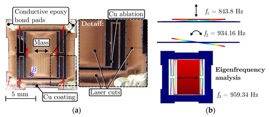
Figure 1.
(a) The manufactured glass magnetometer coated with copper and conductive epoxy bond pads. The copper on the mass was removed by a laser, yielding slits of 10 μm width, which shall guide light through the glass for a future application such as optical detection of modulated light flux. Further, laser cuts on the outer frame interrupts the conductive layer which force an externally applied current over the springs and, hence, over the sensing mass. (b) Simulation results with the frequency of interest at 959.34 Hz (f3).
The transducer’s mass is actuated with the Lorentz force and operated as in-plane resonator at its resonance. Corresponding simulation results are depicted in Figure 1b with the in-plane mode occurring at 959.34 Hz.
The impact of laser cutting is shown in Figure 2. Glass ablation at the center of the mass denotes a too high set laser energy during Cu removal. Further, laser back reflection from the contour cutting step causes glass debris near the cuts and partly Cu ablation. Nevertheless, the surface still provides good conductivity with a measured electrical resistance of 150 Ω between two bond pads.
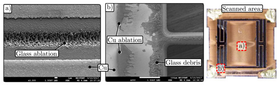
Figure 2.
Detailed SEM photos taken after the transducer manufacturing process. The scanned area at the center of the mass (a) depicts glass ablation caused by too high laser energy. (b) Glass debris from the cutting process and Cu ablation as result of laser back reflection.
3. Measurement Set-Up
Two measurements were performed to characterise the transducer (Figure 3). First, the transducer was mounted onto a custom made shaker unit and excited latteraly at different frequencies. The second measurement was based on a Lorentz force excited transducer. The sensor was placed onto a magnet and an alternating current was applied over the conducting surface yielding a measurable in-plane deflection. The mass’s vibration amplitude of both measurements was recorded optically with a Digital Holographic Microscope DHM®-R2100 Lyncée Tec.
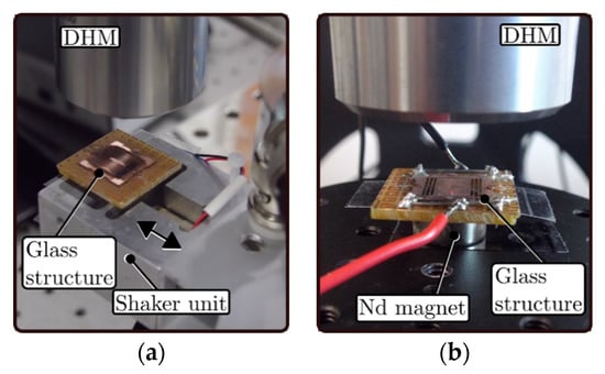
Figure 3.
(a) The transducer is mounted on a piezoelectric driven shaker unit to characterise the structure’s transfer function. (b) Measurement setup for the Lorentz force excited structure, including a neodymium magnet with a magnetic field strength of 100 mT and current supply lines. The in-plane deflection of the transducer’s mass was measured with a Digital Holographic Microscope.
4. Results
Figure 4 depicts the transducer’s transfer functions with an occurring distinctive peak at 940 Hz that approximates the simulation result. Additionally, the shaker’s transfer characteristic was also measured. Further, the structure was excited with a sinusoidal current amplitude IA = 10, 5, 2.5 and 1.75 mA at resonance in presence of a magnetic field, yielding deflections of d =4.23, 2.32, 1.34 and 0.78 µm, respectively. A linear regression calculation reveals an offset of doff = 220 nm at zero excitation current and, thus, demonstrates the transducer’s linear behaviour. Theoretically, the offset for a MEMS resonator comprises the transudcers’s mechanical Brownian noise limit.
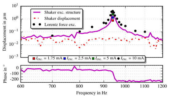
Figure 4.
The plot depicts both, the transducer’s mechanical- and the shaker’s transfer characteristic. Different applied excitation currents at resonance demonstrate the transducer’s linear behavior.
A quality factor of Q =300 was obtained from the measurements with the −3 dB bandwidth method. Mass, stiffness and damping coefficient were estimated from the transfer characteristics and material properties to be m = 18.3 mg, k = 638 N/m and c = 361 × 10−6 kg/s, respectively.
5. Conclusions
Future optimisation of the applied laser energy shall provide more accurate surface patterns, i.e., prevention of glass ablation on the mass and reduction of Cu ablation and glass debris from laser back reflection. Nevertheless, glass based MEMS are promising in applications where electrical insulation and etch resistivity is required or harsh environments such as high temperature applications. Mentionable is the necessity of electrical insulation in distortion-free measurements of the electric field strength based on a small MEMS resonator as published in [7]. Thereby, the SOI mass experiences a force due to electrostatic induction which could be replaced with a glass based MEMS to simplify the technological effort.
Acknowledgments
This work was supported by the country of Lower Austria, the Austrian Science Fund (FWF, project P 28404-NBL) and the prototype funding program PRIZE (project P1621687) of the Austria Wirtschaftsservice Gesellschaft mbH (aws).
Conflicts of Interest
The authors declare no conflict of interest.
References
- Bourhis, E.L. Glass Mechanics and Technology, 2nd ed.; Wiley-VCH: Weinheim, Germany, 2014; ISBN 978-3-527-67944-7. [Google Scholar]
- Bellouard, Y.; Said, A.A.; Dugan, M.; Bado, P. High Accuracy Micro-Displacement Sensor With Integrated Optics-based Detection Means. In Proceedings of the 2005 IEEE International Conference Robotics and Automation, Barcelona, Spain, 18–22 April 2005; pp. 850–854. [Google Scholar] [CrossRef]
- Ripka, P.; Janosek, M. Advances in magnetic field sensors. IEEE Sens. J. 2010, 10, 1108–1116. [Google Scholar] [CrossRef]
- Domke, M.; Egle, B.; Piredda, G.; Stroj, S.; Fasching, G.; Bodea, M.; Schwarz, E. Ultrashort pulse laser dicing of thin Si wafers: the influence of laser-induced periodic surface structures on the backside breaking strength. J. Micromech. Microeng. 2016, 26, 115004. [Google Scholar] [CrossRef]
- Hortschitz, W.; Steiner, H.; Stifter, M.; Kainz, A.; Kohl, F.; Siedler, C.; Schalko, J.; Keplinger, F. Novel MOEMS Lorentz Force Transducer for Magnetic Fields. Procedia Eng. 2016, 168, 680–683. [Google Scholar] [CrossRef]
- Hortschitz, W.; Steiner, H.; Sachse, M.; Stifter, M.; Kohl, F.; Schalko, J.; Jachimowicz, A.; Keplinger, F.; Sauter, T. Robust Precision Position Detection with an Optical MEMS Hybrid Device. IEEE Trans. Ind. Electron. 2012, 59, 4855–4862. [Google Scholar] [CrossRef]
- Kainz, A.; Schalko, J.; Jachimowicz, A.; Keplinger, F.; Steiner, H.; Kohl, F.; Stifter, M.; Beigelbeck, R.; Hortschitz, W. Distortion-free measurement of electric field strength with a MEMS sensor. Nat. Electron. 2018, 1, 68–73. [Google Scholar] [CrossRef] [PubMed]
Publisher’s Note: MDPI stays neutral with regard to jurisdictional claims in published maps and institutional affiliations. |
© 2018 by the authors. Licensee MDPI, Basel, Switzerland. This article is an open access article distributed under the terms and conditions of the Creative Commons Attribution (CC BY) license (https://creativecommons.org/licenses/by/4.0/).