Article

Fast Transformation of PbTe Using a Multiphase Mixture of Precursors: First Insights

by
Hugo Rojas-Chávez
1,*,
Nina Daneu
2,
Manuel A. Valdés-Madrigal
3,
Guillermo Carbajal-Franco
4,
Marcela Achimovičová
5 and
José M. Juárez-García
6,*
1
Tecnológico Nacional de México, Instituto Tecnológico de Tláhuac II, Camino Real 625, Col. Jardines Del Llano, San Juan Ixtayopan, Alcaldía Tláhuac, CDMX 13550, Mexico
2
Advanced Materials Department, Jožef Stefan Institute, Jamova Cesta 39, 1000 Ljubljana, Slovenia
3
Tecnológico Nacional de México, Instituto Tecnológico Superior de Ciudad Hidalgo, Av. Ing. Carlos Rojas Gutiérrez 2120, Ciudad Hidalgo 61100, Mexico
4
Tecnológico Nacional de México, Instituto Tecnológico de Toluca, Division of Graduate Studies and Research, Av. Tecnológico s.n., Metepec Estado de México 52149, Mexico
5
Institute of Geotechnics, Slovak Academy of Sciences, 04001 Košice, Slovakia
6
Universidad Tecnológica del Estado de Querétaro, Industrial Division, 2501 Av. Pie de la Cuesta, Nacional, Santiago de Querétaro 76148, Mexico
*
Authors to whom correspondence should be addressed.
Quantum Beam Sci. 2025, 9(3), 24; https://doi.org/10.3390/qubs9030024
Submission received: 29 May 2025 / Revised: 2 July 2025 / Accepted: 4 July 2025 / Published: 11 July 2025
(This article belongs to the Special Issue New Challenges in Electron Beams)

Abstract

For the first time, a mixture of PbTe and Pb- and Te-oxides coated with carbon, under electron beam irradiation (EBI), was transformed into quantum dots, nanocrystals, nanoparticles and grains of PbTe with a sintered appearance. A small portion of non-stoichiometric phases was also obtained. By selecting conditions that favor the instantaneous transformation, the Gibbs free energy barrier is lowered for obtaining different PbTe structures. The driving force associated with the high-energy milling requires 4 h of processing time to reach a complete transformation, while a high-energy source kinetically affects precursor surfaces to cause an abrupt global chemical transformation instantly. Importantly, the size of the PbTe structures increases as they approach the irradiation point, implying a growth process that is affected by the local temperature reached during the EBI. Imaging after the EBI process revealed morphological variations in PbTe, which can be attractive for use in thermoelectric materials. The results of this study provide the first insights into electron-beam-induced reactions using a multiphase mixture of precursors. Therefore, it is believed that this proposal can also be applied to obtain other binary semiconductor structures, even ternary ones.

1. Introduction

Lead telluride (PbTe) has long been recognized as an IV–VI semiconductor with a rock-salt crystal structure and a relatively narrow band gap [1,2]. Due to its unique size-dependent chemical and physical properties, PbTe has been the subject of extensive investigation for many years [3,4], which is associated with various technological applications [5,6,7], for instance, photo-electrics, telecommunications, photovoltaics and thermoelectric generators [8,9,10]. It is well-known that PbTe nanocrystals (NCs) present pronounced size-dependent optical characteristics due to surface effects and quantum confinement. Smaller PbTe NCs exhibit strong quantum confinement when their size is below the Bohr radius (<50 nm) [3,11]. For this reason, according to literature reports, as the diameter of PbTe NCs decreases, the band gap increases, resulting in a blue shift in the absorption spectrum [12]. However, PbTe-based compounds in various structural forms are among the highest-performing thermoelectrics in the mid-temperature range of 500–900 K [13,14,15].
The properties of PbTe depend on the synthesis route, which affects the reaction kinetics, impacting nucleation, growth mechanisms and final morphology [3,4,16,17,18,19]. Although the melting point of PbTe is relatively high (~924 °C), it can be synthesized near room temperature via high-energy milling (HEM). It is a top-down approach commonly used to produce PbTe micro- and nanoparticles, including quantum-sized materials [4,20]. The HEM provides the thermo-mechanical processes required for completing the synthesis of the desired reaction product from precursors through high-energy collisions [4,21], assuming a direct reaction represented by
M + N E m M N
where ΔEm stands for the energy supplied by the HEM process [21]. A semiconductor compound should be obtained if M and N are considered pure precursors and the milling is carried out in an oxygen-free atmosphere. It is worth mentioning that the reaction kinetics is a function of the amount of ΔEm supplied. Then, as the milling time increases, it becomes significant, indicating a longer processing time based on the nature of the precursors [4,21].
The results reported in the literature provide relevant information about the size, structural and morphological evolution of pure precursors under electron beam irradiation (EBI), using a transmission electron microscope (TEM). This technique uses the electron beam (EB) from the TEM gun as the energy source [16]. It is worth mentioning that EBI can lead to localized heating that affects the structural integrity of materials exposed inside a TEM. Moreover, the notable thermal effects can surpass the melting point of the exposed materials [22]. The key idea behind this method is enabling the particle fragmentation and evaporation of pure materials using a focused EB inside a TEM [23]. Due to the amount of energy that can be supplied during EBI, new methods have emerged for solid-state material synthesis, including organic frameworks [24], molecular nanosheets [25], and nanoparticles [26]. It has been proven that the EBI aids in the synthesis of new materials and can improve the properties and modify the behavior of well-known materials [27,28,29], including morphological changes in pure amorphous metal oxide nanoparticles [30].
To this day, it has been reported that the energy supplied during EBI inside a TEM drives the transformation of pure polycrystalline and single-crystal PbTe into faceted nanoparticles, as well as the rapid fabrication of PbTe NCs [31,32]. Furthermore, pure PbTe NCs surrounded by an amorphous shell have been found to be sensitive to EB exposure, which causes the shell to disappear [33]. The morphology and particle size of the obtained PbTe depend on the chosen TEM parameters, provided the PbTe precursor is pure. In this proposal, a precursor mixture of PbTe and Pb- and Te-oxides for EB exposure is employed for the first time. As a result, quantum dots, NCs, nanoparticles and grains of PbTe with a sintered appearance, as well as non-stoichiometric phases, were obtained. In this study, we explored the usage of EBI for preparing different PbTe structures at different scales, which can enhance their thermoelectric properties through structural modifications. In contrast to the findings reported in the literature, the first insights gained from this work should be useful for future studies, particularly those focusing on understanding how EBI affects the reaction kinetics, its influence on the growth mechanisms and the eventual morphology of PbTe structures, considering a precursor mixture of PbTe and Pb- and Te-oxides. Moreover, it is believed that this proposal can also be applied to other binary semiconductors, even ternary ones.

2. Materials and Methods

2.1. Materials

PbO (5 µm, 99.99 mass%) and Te (50 µm, 99.99 mass%) elemental powders from Aldrich were used as received in a binary combination.

2.2. Sample Preparation and Milling Treatment

Te and PbO powder precursors were mixed in the initial 5:3 PbO:Te mass ratio. After that, the mixture was processed by the HEM process, using ZrO2-spheres (10 mm-Ø balls) as milling media, which were sealed together with the PbO−Te powder mixture into a cylindrical nylamid polymeric vial with hemispheric faces to avoid stagnant zones. It is important to consider an overstoichiometric Te addition due to the presence of oxygen in the milling atmosphere (an internal vial volume of ~60 cm3) [4]. The HEM process was carried out using a high-energy type of ball mill (8000 Mixer/Mill, CertiPrep Inc., Metuchen, NJ, USA) with a fixed ball-to-powder weight ratio of 10:1. It was then carried out for up to 1 h under c-P-T vial conditions reached during milling [4,16,34]. Sampling was then performed by removing the as-milled powders from the vial for further characterization.

2.3. Structural Characterization

X-ray powder diffraction (Siemens D-500 diffractometer (Bruker Analytical XRay Systems, Madison, WI, USA), with a Cu anticathode (40 kV, 30 mA) and a linear detector) was used to examine structural changes in the as-milled samples, collecting diffraction data at room temperature; 0.050° (2θ) increments were used to scan the 20–90° (2θ) angular range and the counting duration was set at 0.5 s⸱step−1.

2.4. Preparation of TEM Specimens and Analysis

The as-milled samples were immersed in 100% ethanol and then they were ultrasonically de-agglomerated to separate aggregates into agglomerates and the last ones into clusters or individual nanoparticle arrangements for transmission electron microscopy (TEM) and selected area electron diffraction (SAED) studies. To prevent electron charging, the samples were additionally coated with carbon. The morphology, particle size and atomic structural information of the as-milled sample after 1 h of milling were analyzed using a JEOL 2100 transmission electron microscope (JEOL, Tokyo, Japan) operated at 200 kV, achieving a point-to-point resolution of 0.27 nm. An acceleration voltage of 200 kV was applied to produce quantum dots, NCs, nanoparticles and grains of PbTe with a sintered appearance, as well as non-stoichiometric phases. The required irradiation time for the formation of such PbTe structures was approximately 5–7 s.

3. Results and Discussion

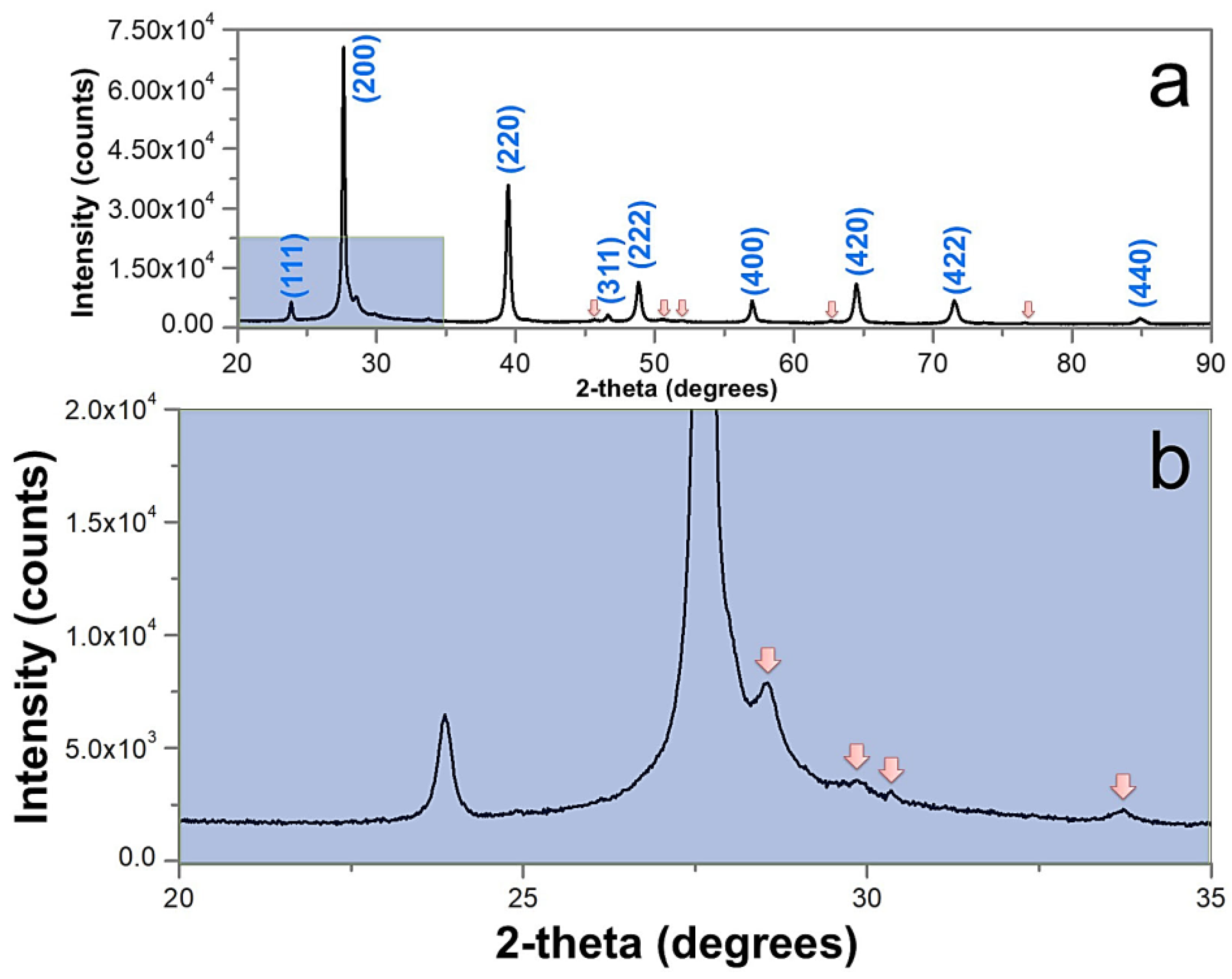
3.1. X-Ray Powder Diffraction

Figure 1 depicts the XRD pattern of the as-milled material under c-P-T vial milling conditions after an hour of processing time. The main Bragg reflections of the as-milled sample were indexed to face-centered cubic PbTe; due to the milling conditions, these reflections present a slight right shift. As shown in Figure 1a, the diffraction peaks were broad and pronounced, the (200) plane demonstrates a predominant orientation. It is important to note that the PbTe compound was identified during the initial milling stage.
The arrows indicate evidence of secondary phases associated with small Pb- and Te-oxide peaks, as shown in Figure 1a,b. For instance, Figure 1b reveals a multiphase structure in the angular region of 27.5° ≤ 2θ ≤ 31.0°. This structure includes peaks from the α-PbO, β-PbO, and Pb3O4 phases, as well as the PbTe contribution, which is consistent with data reported in the literature [35,36]. Furthermore, within the angular region of 27.5° ≤ 2θ ≤ 31.0°, evidence of the α-TeO2 and PbTeO3 phases, associated with small peaks, has been found [37,38]. As Figure 1b shows, these phases overlap in the mentioned angular region. Additionally, small peaks associated with the referred phases appear at 2θ values of approximately 33.7°, 45.6°, 46.6°, 50.5°, 51.9°, 62.6°, and 76.6°. This fact unequivocally establishes that the precursor to be used during EBI is a multiphase mixture.

3.2. TEM Analysis

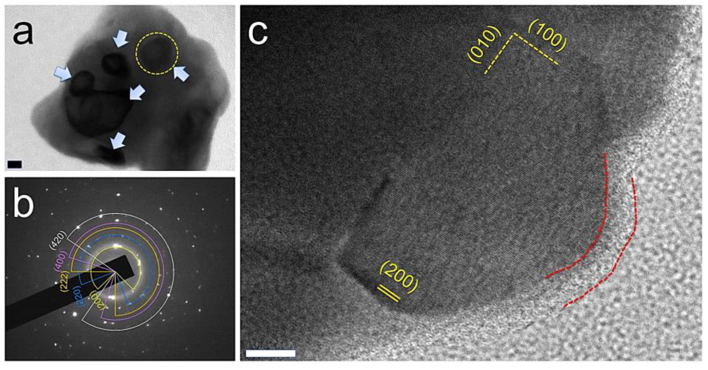
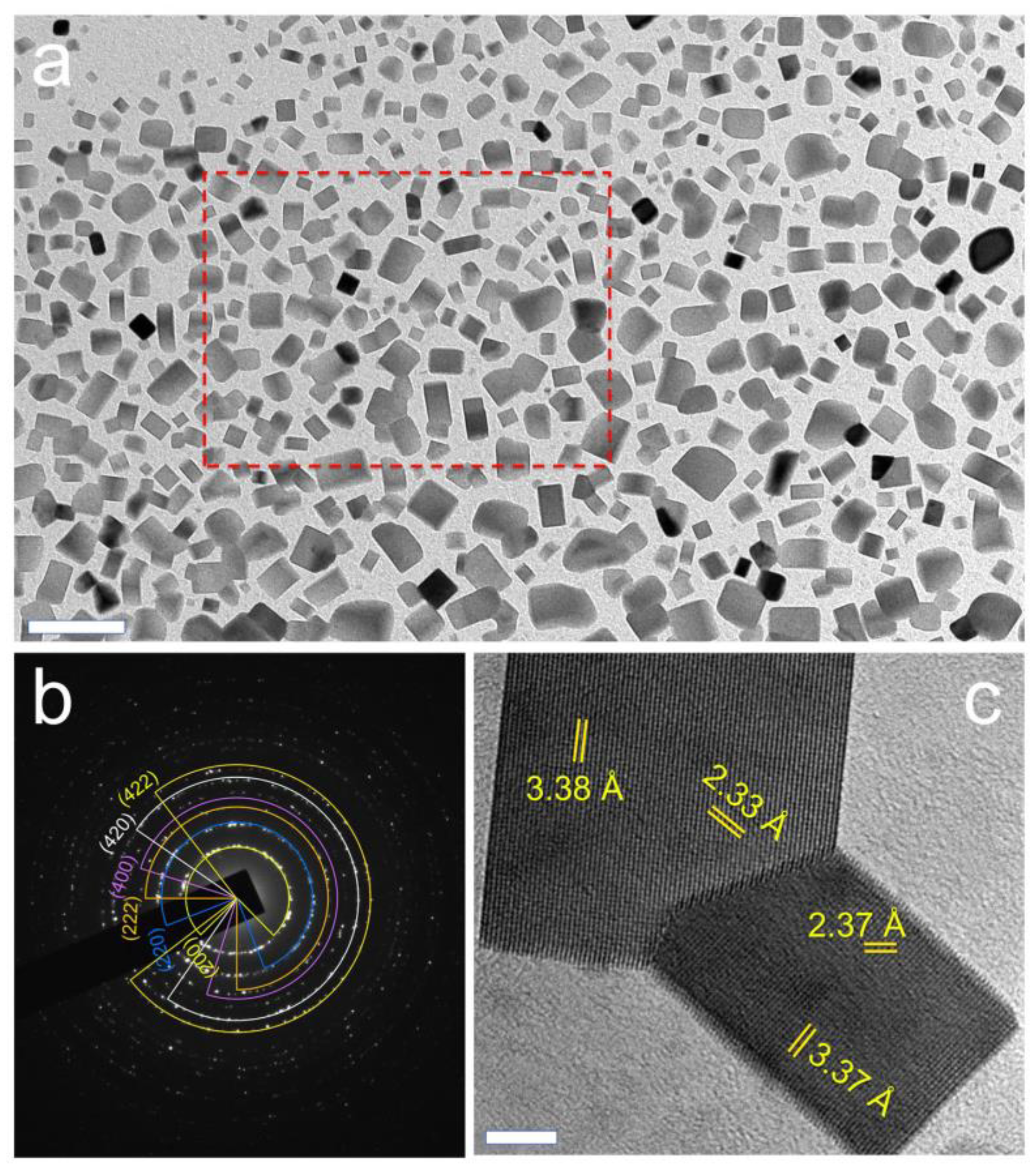
3.2.1. Before Blasting the Multiphase Mixture with an Electron Beam

TEM characterization allowed us to identify the morphology of the as-milled multiphase mixture and how it was arranged after one hour of processing time. Figure 2a shows that the HEM process gives way to the formation of a larger micrometer-sized aggregate. It consists of submicrometer-sized agglomerates ranging in size from 150 nm (blue dashed line) to approximately 1 μm (red dashed line). It is notable that the agglomerates remained in the sample even after ultrasonic dispersion, unless stronger forces overcome them.
Figure 2b is a magnified TEM image of the yellow dashed zone in Figure 2a. It is a typical TEM image of smaller submicrometer-sized clusters. This figure reveals that particles tend to agglomerate, forming clusters through the coalescence of smaller particles. In the upper part of Figure 2b, a single cluster covered by an amorphous thin layer is shown, while in the middle part of the same figure, the occurrence of embedded nanoparticles as well as an amorphous layer about 20 nm in size is revealed. As indicated by the arrows in Figure 2b, these nano-sized particles have a rounded appearance. As shown by the framed zone (red dashed line) in Figure 2b, during milling, different nanostructures were brought into intimate contact via an amorphous layer as long as 6 nm. Such amorphous layers can be attributed to the deposition of vapor phases induced during milling [21]. In this case, however, it could correspond to the carbon applied to prevent charging.
Figure 3a shows that clusters are constituted by a crystalline matrix and an amorphous portion, the arrows reveal that nano-sized crystalline PbTe particles, with a size range of 20 to 50 nm, are embedded within the cluster. The largest number of PbTe particles are less than 50 nm in diameter, which are distinguished by an irregular and rounded shape.
Figure 3b shows a typical SAED pattern obtained from one of the smaller PbTe clusters, confirming that the crystalline particles are PbTe nanoparticles (PDF #781905). The SAED result was consistent with experimental findings obtained via XRD analysis. It is worth noting that TEM/EDS analyses performed on the PbTe particles revealed a Pb:Te atomic ratio very close to 1:1, but the amorphous portion occasionally exhibited a slight tendency to favor Pb.
Though most of the PbTe particles have irregular rounded shapes, Figure 3c shows that some PbTe particles have developed the characteristic cubic morphology. As shown in the same figure, the PbTe particles have partially developed the {100} faces. It is worth keeping in mind that due to the preference for cubic morphologies in surface energy minimization, achieving large spherical PbTe nanoparticles can be challenging because they tend to take on cubic geometries when particle sizes surpass 10 nm [3]. Additionally, the presence of amorphous layers with a size of approximately 6 nm in the cubic PbTe nanoparticles is notable, as indicated by the red dashed lines in Figure 3c. The TEM analyses revealed no other phases in the sample besides the nano-sized PbTe crystallites and amorphous layers.

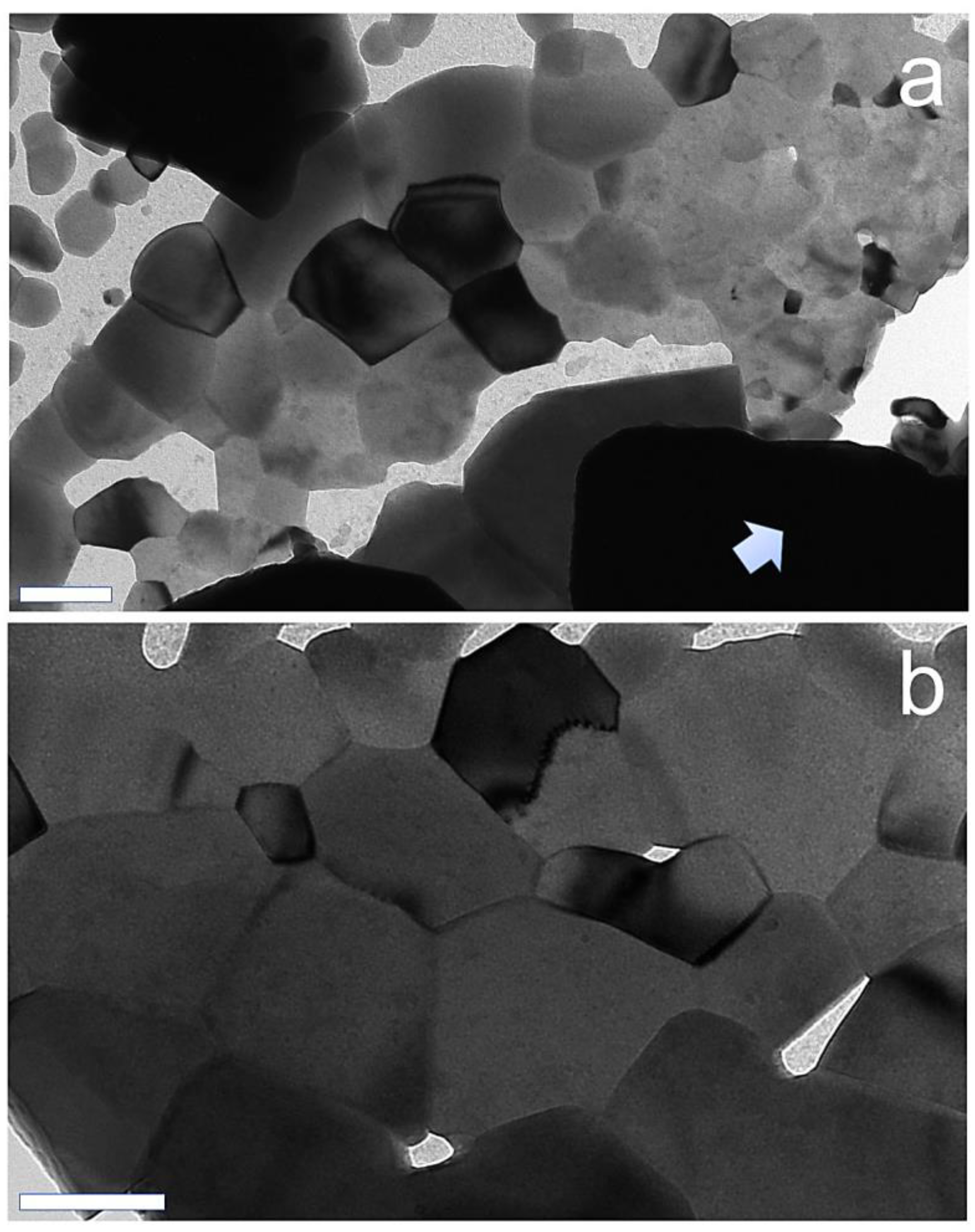
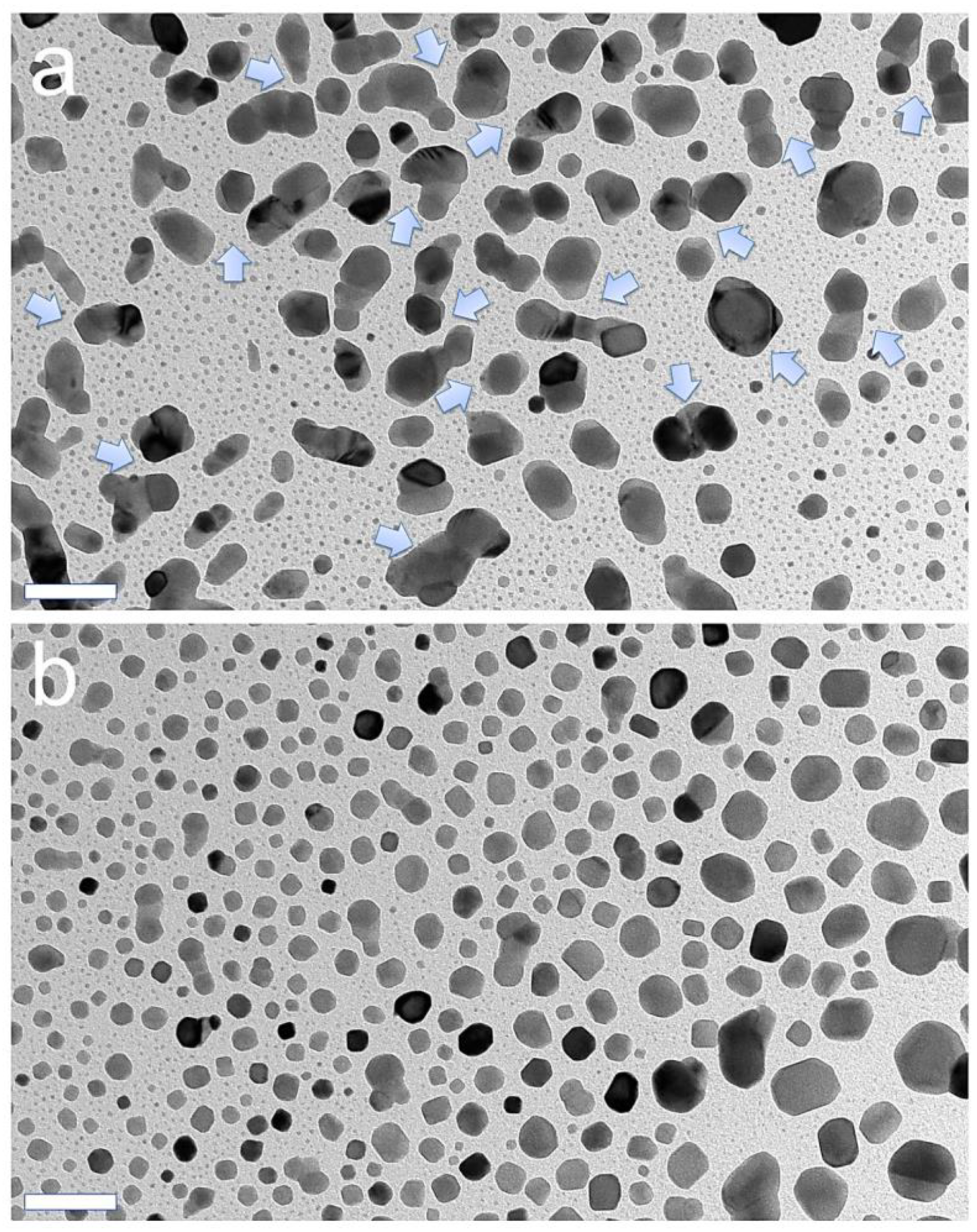
3.2.2. After Blasting the Multiphase Mixture with an Electron Beam

Figure 4 clearly shows the fragmentation of the multiphase mixture after EBI. Interestingly, as shown in Figure 4a, when the initial multiphase mixture, constituted by powdered aggregate microparticles, was exposed to EBI, it gave way to several rounded and faceted grains with a sintered appearance, which formed extremely quickly. It has been reported that the particle formation via EBI is influenced by local temperature, and it is affected by the distance from the irradiation point [22,32]. The EDS analysis of the material, indicated by the arrow in Figure 4a, revealed that it contains only lead (Pb) and oxygen (O). A comparative analysis shows that the typical grain size of the multiphase mixture after EBI lies within the range of ~30 to ~170 nm; see Figure 4a,b. As reported in the literature, in the process of spark plasma sintering, the size of the grains in a nanostructured material is correlated with their dispersion [39]. Therefore, it is inferred that the smaller powder dispersion in the multiphase mixture, after EBI, leads to smaller grains in the resulting nanostructured material due to the local temperature distribution during EBI [32,40]. Consequently, the regions far apart from the faceted grains showed only tiny particles. Furthermore, Figure 4b shows that secondary recrystallization occurs with intensive growth of larger faceted grains at the expense of smaller ones. As grain size increases during grain growth, it is expected that the driving force will decrease, as will the curvature of the grain boundary [41]. Consequently, the irradiated sample in the analyzed area is expected to have a higher relative density due to a reduction in void space between grains; see Figure 4b.
Interconnected particles with a sintered appearance were observed close to the faceted grains. A thorough analysis of this area provides further insights into these particles. As Figure 5a shows, it is composed of numerous interconnected particles surrounded by nanoparticles and quantum dots of different sizes produced by the EB after irradiation. As indicated by the arrows in Figure 5a, it can be inferred that the interconnected particles tend to form faceted grains with a sintered appearance. The size and number of these grains are expected to decrease with increasing distance from the initial irradiated aggregate due to the local temperature distribution during EBI [31,41].
As shown in Figure 5b, it was clearly observed that the as-formed interconnected particles tended to decrease in size in regions far apart from the primary aggregate [41]. Moreover, the process was accompanied by the formation of spherical nanoparticles that tended to be pseudocubic after EB exposure. Therefore, it is believed that the spherical nanoparticles may have facilitated the growth of faceted PbTe NCs; see Figure 5b. It is important to keep in mind that, due to the preference for cubic morphologies in surface energy minimization, it can be challenging to achieve large spherical PbTe nanoparticles when their sizes surpass 10 nm [3]. Consequently, as shown in Figure 5b, the coexistence of quantum dots, pseudocubic, rounded and perfect faceted nanoparticles are demonstrated. For the sake of clarity, all these particles are depicted separately in Figure 6.
Focusing the EB on the aggregate regularly resulted in perfect faceted nanoparticles; see Figure 6a. This occurred even when the largest condenser aperture was used for HRTEM analyses. Therefore, the analysis of the as-formed PbTe faceted nanoparticles required the use of a smaller condenser aperture. As shown in Figure 6a, three types of morphologies are usually formed, namely, rounded, pseudocubic and perfect faceted nanoparticles. It is important to mention that faceted nanoparticles and perfect PbTe cubes with sizes of about 50 nm were obtained. It is noteworthy that the as-formed PbTe nanoparticles have a polycrystalline structure, as confirmed by the concentric circles in Figure 6b. Furthermore, the SAED pattern of the irradiated sample reveals a new plane that corresponds to the (422) plane associated with the PbTe phase. Along with this, the SAED pattern confirms the crystallinity of the as-formed PbTe nanoparticles; see Figure 6b.
Following EBI, a large number of faceted PbTe nanoparticles covered the area around the source aggregate. Figure 6c shows an HRTEM image of one of the thinner particles from Figure 6a. The clear lattice fringes indicate that there is no lattice disorder in the faceted PbTe nanoparticles obtained after EBI. The fringe spacings of 3.37 Å, 3.38 Å, 2.33 Å, and 2.37 Å align closely with the (200) and (220) lattice plane spacings of PbTe. As energy was supplied, the interaction between the EB and matter caused faceted nanoparticles with a [100] orientation, which were attached to each other; see Figure 6c. After that, they bond with each other and partially give way to larger particles. Another experimental finding is that such faceted PbTe nanoparticles are perfectly oriented and attached to each other without edge dislocations [4,34].

4. Conclusions

A multiphase mixture of PbTe and Pb- and Te-oxides was studied for the first time as an alternative precursor under electron beam irradiation, using a transmission electron microscope. In contrast to pure PbTe precursors used during EBI, such a multiphase mixture, coated with carbon, is the first precursor that combines a series of oxides with PbTe. At the required accelerating voltage of 200 kV, the irradiation time is long enough to obtain quantum dots, nanocrystals, nanoparticles and grains of PbTe with a sintered appearance, including a small portion of non-stoichiometric phases. The precursor depletion was the mechanism through which the transformation was achieved. It is inferred that due to the local temperature reached during EBI, the as-formed PbTe structures diminish in size with increasing distance from the irradiation point. The driving force associated with the milling process produces larger micrometer-sized aggregates containing agglomerates and clusters with embedded PbTe nanoparticles. Conversely, significant dimensional, morphological, and stoichiometric changes may suddenly occur when the conditions of a high-energy source, vacuum, and precursors are fully met. We hope that the experimental findings presented here will help answer questions about the nature of precursor effects in future research. Nevertheless, further experiments are needed to deeply understand the global chemical transformations of different PbTe nanostructures for applications that require various morphological and structure forms, as in the case of thermoelectric materials.

Author Contributions

Conceptualization, H.R.-C., J.M.J.-G., N.D. and M.A.; methodology, H.R.-C., J.M.J.-G., N.D., M.A. and M.A.V.-M.; formal analysis, H.R.-C., J.M.J.-G., N.D., M.A. and G.C.-F.; investigation, H.R.-C., J.M.J.-G. and M.A.V.-M.; writing—original draft preparation, H.R.-C. and J.M.J.-G.; writing—review and editing, H.R.-C., J.M.J.-G. and G.C.-F.; funding acquisition, H.R.-C. and J.M.J.-G. All authors have read and agreed to the published version of the manuscript.

Funding

This research received no external funding.

Data Availability Statement

Data are contained within the article.

Acknowledgments

H.R.-C., J.M.J.-G., G.C.-F. and M.A.V.-M. thank the Sistema Nacional de Investigadoras e Inves-tigadores (SNII) for the designation.

Conflicts of Interest

The authors declare no conflicts of interest.

Abbreviations

The following abbreviations are used in this manuscript:
EBElectron beam
EBIElectron beam irradiation
HEMHigh-energy milling
TEMTransmission electron microscopy
XRDX-ray diffraction

References

  1. Jiang, Y.; Pei, C.; Wang, Q.; Wu, J.; Zhang, L.; Xiong, C.; Qi, Y. Pressure-Induced Superconductivity and Phase Transition in PbSe and PbTe. Chin. Phys. B 2024, 33, 126105. [Google Scholar] [CrossRef]
  2. Wang, L.; Li, G.; Jiang, Y.; Ma, H.; Deng, S.; Deng, S. Anionic Isoelectronic Substitution Effects on Thermal Stability and Thermoelectric Performance of PbTe-PbSe Compounds. J. Electron. Mater. 2025, 54, 6300–6314. [Google Scholar] [CrossRef]
  3. Lyssenko, S.; Amar, M.; Sermiagin, A.; Barbora, A.; Minnes, R. Tailoring PbTe quantum dot Size and morphology via ligand composition. Sci. Rep. 2025, 15, 2630. [Google Scholar] [CrossRef] [PubMed]
  4. Rojas-Chávez, H.; Miralrio, A.; Cruz-Martínez, H.; Carbajal-Franco, G.; Valdés-Madrigal, M.A. Oriented-Attachment- And Defect-Dependent PbTe Quantum Dots Growth: Shape Transformations Supported by Experimental Insights and DFT Calculations. Inorg. Chem. 2021, 60, 7196. [Google Scholar] [CrossRef]
  5. Chen, T.; Shao, Y.; Feng, R.; Zhang, J.; Wang, Q.; Dong, Y.; Ma, H.; Sun, B.; Ao, D. Enhancing the Thermoelectric Performance of n-Type PbTe via Mn Doping. Materials 2025, 18, 1029. [Google Scholar] [CrossRef]
  6. Gao, P.; Chen, X.; Liu, Z.; An, W.; Wang, N. Theoretical Investigation of the Ultralow Thermal Conductivity of 2D PbTe via a Strain Regulation Method. Phys. Chem. Chem. Phys. 2025, 27, 10198–10208. [Google Scholar] [CrossRef]
  7. Rojas-Chávez, H.; Pineda, A.J.M.; Garcia, J.M.J.; Cruz-Martínez, H.; Montejo-Alvaro, F. Theoretical Study of the Adsorption Modes of a Process Control Agent in the Growth of PbTe. Rev. Mex. Física 2025, 71, 011004. [Google Scholar] [CrossRef]
  8. Deng, Q.; Tan, X.; Wen, J.; Li, R.; Luo, J.; Xie, Y.; Zhao, Z.; Sa, B.; Ang, R. Ultra-High Thermoelectric Performance in Ternary n-Type PbTe Collaboratively Enabled by Self-Optimized Carrier Concentration and Ultra-Low Lattice Thermal Conductivity. J. Mater. Sci. Technol. 2025, 236, 86–94. [Google Scholar] [CrossRef]
  9. Guo, W.; Ran, Y.; Han, J.; Wang, S.; Ning, X. PbTe Films with In-Plane Random Orientation: Viable Alternatives for Room-Temperature Thermoelectric Generators. J. Alloys Compd. 2025, 1021, 179635. [Google Scholar] [CrossRef]
  10. Ma, L.; Song, L.; Zheng, Z.; Lan, Y.; Zhou, L.; Liu, R.; Li, Y.; Wei, Z.; Wu, S.; Shi, Y.; et al. Optimizing the Cooling Performance of Lead Telluride by Doping Silver. Solid. State Sci. 2025, 162, 107859. [Google Scholar] [CrossRef]
  11. Ten Kate, S.C.; Ritter, M.F.; Fuhrer, A.; Jung, J.; Schellingerhout, S.G.; Bakkers, E.P.A.M.; Riel, H.; Nichele, F. Small Charging Energies and G-Factor Anisotropy in PbTe Quantum Dots. Nano Lett. 2022, 22, 7049–7056. [Google Scholar] [CrossRef] [PubMed]
  12. Peters, J.L.; de Wit, J.; Vanmaekelbergh, D. Sizing Curve, Absorption Coefficient, Surface Chemistry, and Aliphatic Chain Structure of PbTe Nanocrystals. Chem. Mater. 2019, 31, 1672–1680. [Google Scholar] [CrossRef] [PubMed]
  13. Jarashneli, A.; Towe, E.; Auslender, M.; Kovalyuk, V.; Goltsman, G.; Dashevsky, Z. Development of Regular Vertical P-n Junction on Nanocrystalline PbTe Film. J. Appl. Phys. 2025, 137, 105302. [Google Scholar] [CrossRef]
  14. Skelton, J.M.; Parker, S.C.; Togo, A.; Tanaka, I.; Walsh, A. Thermal Physics of the Lead Chalcogenides PbS, PbSe, and PbTe from First Principles. Phys. Rev. B 2014, 89, 205203. [Google Scholar] [CrossRef]
  15. Li, Y.; Bi, H.; Du, Y.; Che, R. Synthesis and Thermoelectric Properties of Defect-Containing PbSe–PbTe Heterojunction Nanostructures. RSC Adv. 2017, 7, 53855–53860. [Google Scholar] [CrossRef]
  16. Rojas-Chávez, H.; Miralrio, A.; Juárez-García, J.M.; Carbajal-Franco, G.; Cruz-Martínez, H.; Montejo-Alvaro, F.; Valdés-Madrigal, M.A. A Comparative DFT Study on Process Control Agents in the Mechanochemical Synthesis of PbTe. Int. J. Mol. Sci. 2022, 23, 11194. [Google Scholar] [CrossRef]
  17. Park, S.; Ryu, B.; Park, S. Off-Centered Pb Interstitials in PbTe. Materials 2022, 15, 1272. [Google Scholar] [CrossRef]
  18. Yu, H.; Zu, Y.; Gao, L.; Zaheer Ud Din, S.; Li, C.; Gao, H.; Ji, W.; Xu, H.; Zhai, R.; Jia, Z.; et al. Zero-Dimensional Lead Telluride Quantum Dots Optical Modulator for Red Pr:YLF Ultrashort Pulse Laser. Opt. Laser Technol. 2025, 181, 112003. [Google Scholar] [CrossRef]
  19. Senapati, P.; Parida, P. Thermoelectric performance of quantum dots embedded in an Aharonov-Bohm ring: A Pauli master equation approach. Sci. Rep. 2025, 15, 13232. [Google Scholar] [CrossRef]
  20. Chen, Z.; Zhao, C.; Zhou, X.; Xiao, L.; Li, Z.; Zhang, Y. A Review of Top-Down Strategies for the Production of Quantum-Sized Materials. Small Sci. 2023, 3, 2300086. [Google Scholar] [CrossRef]
  21. Rojas-Chávez, H.; Reyes-Carmona, F.; Garibay-Febles, V.; Jaramillo-Vigueras, D. Solid–Solid and Gas–Solid Interactions Induced during High-Energy Milling to Produce PbTe Nanopowders. J. Nanopart. Res. 2013, 15, 1623. [Google Scholar] [CrossRef]
  22. Lee, S.B.; Kwon, J.; Yoo, S.J.; Kim, H.S. Lattice Destabilization in Electron-Beam-Irradiated Antimony in TEM. Mater. Charact. 2024, 212, 114008. [Google Scholar] [CrossRef]
  23. Lian, L.; Cheng, F.; Xia, Y.; Zheng, M.; Ke, J.; Zhang, W.; He, J.; Liu, H.; Zhang, D.; Gao, J.; et al. Electron Beam Induced Formation of Hollow RbBr Nanocubes. J. Phys. Chem. C 2018, 122, 28347–28350. [Google Scholar] [CrossRef]
  24. Zhang, M.; Chen, J.; Zhang, S.; Zhou, X.; He, L.; Sheridan, M.V.; Yuan, M.; Zhang, M.; Chen, L.; Dai, X.; et al. Electron Beam Irradiation as a General Approach for the Rapid Synthesis of Covalent Organic Frameworks under Ambient Conditions. J. Am. Chem. Soc. 2020, 142, 9169–9174. [Google Scholar] [CrossRef]
  25. Neumann, C.; Wilhelm, R.A.; Küllmer, M.; Turchanin, A. Low-Energy Electron Irradiation Induced Synthesis of Molecular Nanosheets: Influence of the Electron Beam Energy. Faraday Discuss. 2021, 227, 61–79. [Google Scholar] [CrossRef]
  26. Weinel, K.; Hahn, M.B.; Lubk, A.; Feng, W.; Gonzalez Martinez, I.G.; Büchner, B.; Agudo Jácome, L. Nanoparticle Synthesis by Precursor Irradiation with Low-Energy Electrons. ACS Appl. Nano Mater. 2025, 8, 4980–4988. [Google Scholar] [CrossRef]
  27. Arnold, M.; Katzmann, J.; Naik, A.; Görne, A.L.; Härtling, T.; George, J.; Schuster, C. Investigations on Electron Beam Irradiated Rare-Earth Doped SrF2 for Application as Low Fading Dosimeter Material: Evidence for and DFT Simulation of a Radiation-Induced Phase. J. Mater. Chem. C 2022, 10, 11579–11587. [Google Scholar] [CrossRef]
  28. Chen, J.; Zhang, M.; Shu, J.; Yuan, M.; Yan, W.; Bai, P.; He, L.; Shen, N.; Gong, S.; Zhang, D.; et al. Electron Beam Irradiation-Induced Formation of Defect-Rich Zeolites under Ambient Condition within Minutes. Angew. Chem. Int. Ed. 2021, 60, 14858–14863. [Google Scholar] [CrossRef]
  29. Ghobashy, M.M.; Sharshir, A.I.; Zaghlool, R.A.; Mohamed, F. Investigating the Impact of Electron Beam Irradiation on Electrical, Magnetic, and Optical Properties of XLPE/Co3O4 Nanocomposites. Sci. Rep. 2024, 14, 4829. [Google Scholar] [CrossRef]
  30. Latham, A.H.; Williams, M.E. Transmission Electron Microscope-Induced Structural Evolution in Amorphous Fe, Co, and Ni Oxide Nanoparticles. Langmuir 2008, 24, 14195–14202. [Google Scholar] [CrossRef]
  31. Zelenina, I.; Veremchuk, I.; Grin, Y.; Simon, P. In Situ Observation of Electron-Beam-Induced Formation of Nano-Structures in PbTe. Nanomaterials 2021, 11, 163. [Google Scholar] [CrossRef] [PubMed]
  32. Hu, J.; Sun, Y.; Chen, Z. Rapid Fabrication of Nanocrystals through in Situ Electron Beam Irradiation in a Transmission Electron Microscope. J. Phys. Chem. C 2009, 113, 5201–5205. [Google Scholar] [CrossRef]
  33. Falqui, A.; Bertoni, G.; Genovese, A.; Marras, S.; Malerba, M.; Franchini, I.R.; Manna, L. Electron Microscopy Studies of Electron-Beam Sensitive PbTe-Based Nanostructures. Microsc. Res. Tech. 2010, 73, 944–951. [Google Scholar] [CrossRef] [PubMed]
  34. Rojas-Chávez, H.; Carbajal-Franco, G.; Cruz-Martínez, H.; Juárez-García, J.M. Insights into the Mechanochemical Synthesis of Nanostructured PbTe: The Role of Structural Defects. Mater. Lett. 2024, 370, 136807. [Google Scholar] [CrossRef]
  35. Rojas-Chávez, H.; Díaz-de la Torre, S.; Jaramillo-Vigueras, D.; Plascencia, G. PbTe Mechanosynthesis from PbO and Te. J. Alloys Compd. 2009, 483, 275–278. [Google Scholar] [CrossRef]
  36. Mourad, M.M.; Sharshar, T.; Ghali, M.; Abdou, Y.; Elhussiny, F.; Hemeda, O.M.; Badran, H.M. Effect of Mechanical Ball Milling on the Microstructure and Radiation Shielding Performance of Nano-PbO. Chem. Phys. 2025, 591, 112542. [Google Scholar] [CrossRef]
  37. Han, L.; Liu, C.; Wang, X.; Li, F.; Fan, C.; Zhang, J. Low-Temperature Aqueous Solution Growth of the Acousto-Optic TeO2 Single Crystals. Mater. Adv. 2024, 5, 3022–3028. [Google Scholar] [CrossRef]
  38. Weil, M.; Shirkhanlou, M.; Füglein, E.; Libowitzky, E. Determination of the Correct Composition of “Hydrous Lead(II) Oxotellurate(IV)” as PbTeO3, Crystallizing as a New Polymorph. Crystals 2018, 8, 51. [Google Scholar] [CrossRef]
  39. Sherchenkov, A.; Borgardt, N.; Shtern, M.; Zaytseva, Y.; Shtern, Y.; Rogachev, M.; Sazonov, V.; Yakubov, A.; Pepelyaev, D. The Role of Nanostructuring Strategies in PbTe on Enhancing Thermoelectric Efficiency. Mater. Today Energy 2023, 37, 101416. [Google Scholar] [CrossRef]
  40. Kim, H.B.; Jeun, J.P.; Kang, P.H.; Oh, S.-H. Fabrication of Carbon Layer Coated FE-Nanoparticles Using an Electron Beam Irradiation. Radiat. Phys. Chem. 2016, 118, 2–5. [Google Scholar] [CrossRef]
  41. Karansky, V.V.; Klimov, A.S.; Smirnov, S.V. Structural Transformations in Mn–Zn Ferrite under Low-Energy Electron Beam Treatment. Vacuum 2020, 173, 109115. [Google Scholar] [CrossRef]
Figure 1. (a) XRD pattern of the as-milled sample after 1 h of milling. Note that the Miller indices on the upper diffraction pattern correspond to the PbTe compound. (b) Zoomed area of the framed zone in (a) in the range 20–35°.
Qubs 09 00024 g001
Figure 2. (a) Typical low-resolution TEM image of a larger micrometer-sized aggregate in the multiphase mixture after 1 h of processing time (black dashed line); it is constituted by submicrometer-sized agglomerates (blue dashed line), which reach 1 μm in size (red dashed line). Scale bar: 200 nm. (b) Magnified image of the framed zone (yellow dashed line) in (a), the arrows reveal the presence of embedded nanoparticles. Scale bar: 50 nm.
Qubs 09 00024 g002
Figure 3. (a) Typical TEM image of a cluster in the multiphase mixture after 1 h of processing time, the arrows reveal the presence of nano-sized crystalline PbTe particles, one of which is circled in yellow. (b) Selected area electron diffraction pattern recorded on the particles in (a). (c) PbTe nanoparticle with partially developed {100} faces in the multiphase mixture after 1 h of processing time. In the (a,c) images, the scale bars are 10 nm.
Qubs 09 00024 g003
Figure 4. (a) TEM image of the multiphase mixture after electron beam irradiation, the arrow indicates where the EDS analysis was performed. (b) The same sample after electron beam irradiation was increased in grain size. In both images, the scale bars are 100 nm.
Qubs 09 00024 g004
Figure 5. (a) TEM image of the as-formed PbTe interconnected particles, indicated by the arrows, after electron beam irradiation. (b) TEM image of the as-formed PbTe nanoparticles after electron beam irradiation. In both images, the scale bars are 100 nm.
Qubs 09 00024 g005
Figure 6. (a) TEM image of the as-formed PbTe nanoparticles after electron beam irradiation. Scale bar: 100 nm. (b) Selected area electron diffraction pattern recorded on the framed area (red dashed line) in the nanostructure shown in (a). (c) HRTEM image of faceted PbTe nanostructures along the [100] zone axis. Scale bar: 5 nm.
Qubs 09 00024 g006
Disclaimer/Publisher’s Note: The statements, opinions and data contained in all publications are solely those of the individual author(s) and contributor(s) and not of MDPI and/or the editor(s). MDPI and/or the editor(s) disclaim responsibility for any injury to people or property resulting from any ideas, methods, instructions or products referred to in the content.

