1. Introduction
A surface plasmon polariton (SPP) is an electromagnetic wave that propagates on the interface between a dielectric and metal medium [
1]. It is the result of the coupling between the light and collective oscillations of free electrons at the surface of metal. The optical waveguides based on the SPP show an excellent capability in a tight mode confinement, but their propagation length is limited due to ohmic loss and surface scattering caused by imperfections in the fabrication. Various types of SPP waveguides for guiding the surface plasmon waves have been proposed and investigated theoretically and experimentally in the literature. The purpose is to overcome the trade-off between the high mode confinement and the low loss propagation. The possibility of an electromagnetic energy concentration and low loss propagation fundamentally depends on the geometrical structure of the SPP waveguide. Typical SPP waveguide structures are reported in the literature, such as metallic nanowires [
2,
3], metal strips [
4,
5], an array of metal nanoparticles [
6], V–shaped waveguides [
7,
8] and wedge-shaped waveguides [
9,
10,
11]. The structure of an SPP waveguide usually consists of a thin metallic layer deposited directly on a dielectric or separated from a dielectric by an insulator. The SPP waveguides can be found in various applications, such as light signal guiding far beyond the diffraction limit [
12,
13,
14], biosensors [
15,
16,
17] or refractive index sensing sensors [
18]. For sensing applications, it requires not only a low-loss SPP wave propagation, but also the direct interaction of SPP waves with detected objects.
Recent research has been devoted to wedge SPP waveguide structures due to the excellent capability of tight mode confinement around the apex of a metallic wedge. The wedge SPP waveguides can be realized by using low refractive index materials such as polymers as a dielectric or electrically active materials such as graphene. However, in order to integrate with electronic components, the SPP waveguides require in terms of the materials that their fabrication process is compatible with the standard complementary metal-oxide semiconductor (CMOS) technology. Silicon is considered as a natural choice for constructing SPP waveguides due to its well-established CMOS compatible fabrication technology. Moreover, silicon with a high refractive index enables further spatial confinement of the SPP mode and makes the waveguide cross section even more compact. Silicon-based SPP waveguides can be fabricated by dry etching or wet etching. Recently, there have been several reports on wedge-shaped silicon waveguides based on the anisotropic wet etching property of single crystal silicon [
19,
20,
21]. However, the exploration of wedge silicon SPP waveguides based on the anisotropic wet etching property has not yet been reported. Moreover, a comprehensive analysis of the performance of the wedge silicon SPP waveguides is necessary to provide guidelines for the design and fabrication of a wedge SPP waveguide with an optimal performance.
In this paper, we propose wedge SPP waveguides and investigate their propagation characteristics. The wedge SPP waveguides with an atom-level smooth surface can be fabricated by exploring the wet anisotropic etching property of single crystal silicon in a potassium hydroxide (KOH) solution. The smooth surface plays an important role in low loss surface plasmon wave propagation due to low surface scattering. The propagation characteristics of the wedge SPP waveguide at the optical telecommunication wavelength are investigated by a numerical simulation. In this work, we also analyze and compare comprehensively the propagation characteristics of wedge SPP waveguides, from which the wedge SPP waveguide with an optimal performance is derived.
2. Wedge SPP Waveguides and Model for Simulation
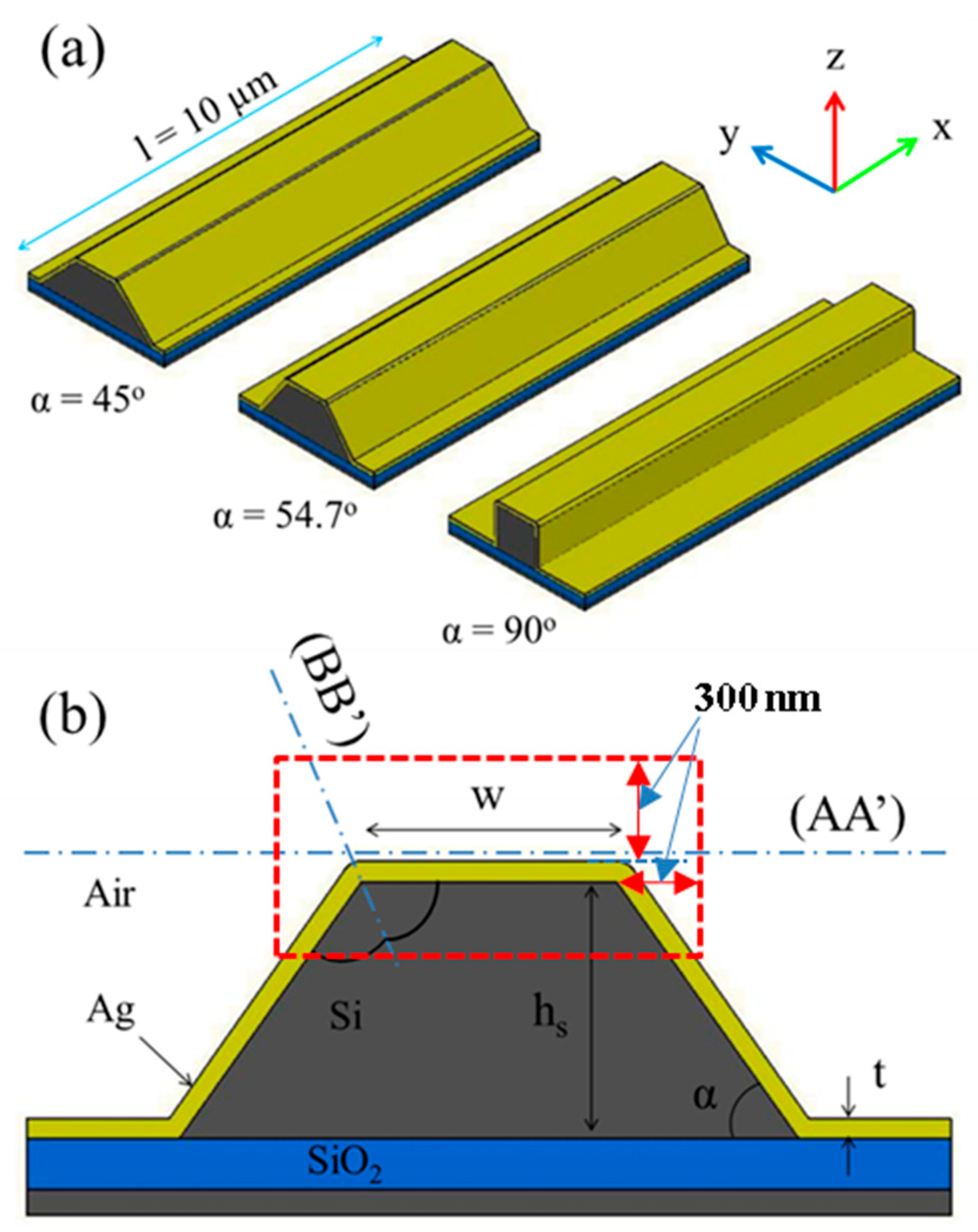
The geometry of the proposed wedge SPP waveguides is shown in
Figure 1. The wedge SPP waveguides consist of an Ag thin metallic film deposited onto the surface of wedge–shaped silicon waveguides, which is embedded in air or in a different interaction environment. Two wedge plasmon polariton (WPP) modes propagate on the two edges of the wedge SPP waveguide structures. The sidewall corner
α of the silicon waveguide can be 35.26°, 45°, 54.74° or 90°, which are proposed on the basis of exploring the wet anisotropic etching property of single crystal silicon in a KOH solution [
19,
20,
22].
The important part of the wedge SPP waveguide is the silicon waveguide that forms the shape and size of the wedge SPP waveguide. The silicon waveguides can be realized by dry etching using focus ion beam micromachining [
23], reactive ion etching [
24] or wet etching [
19,
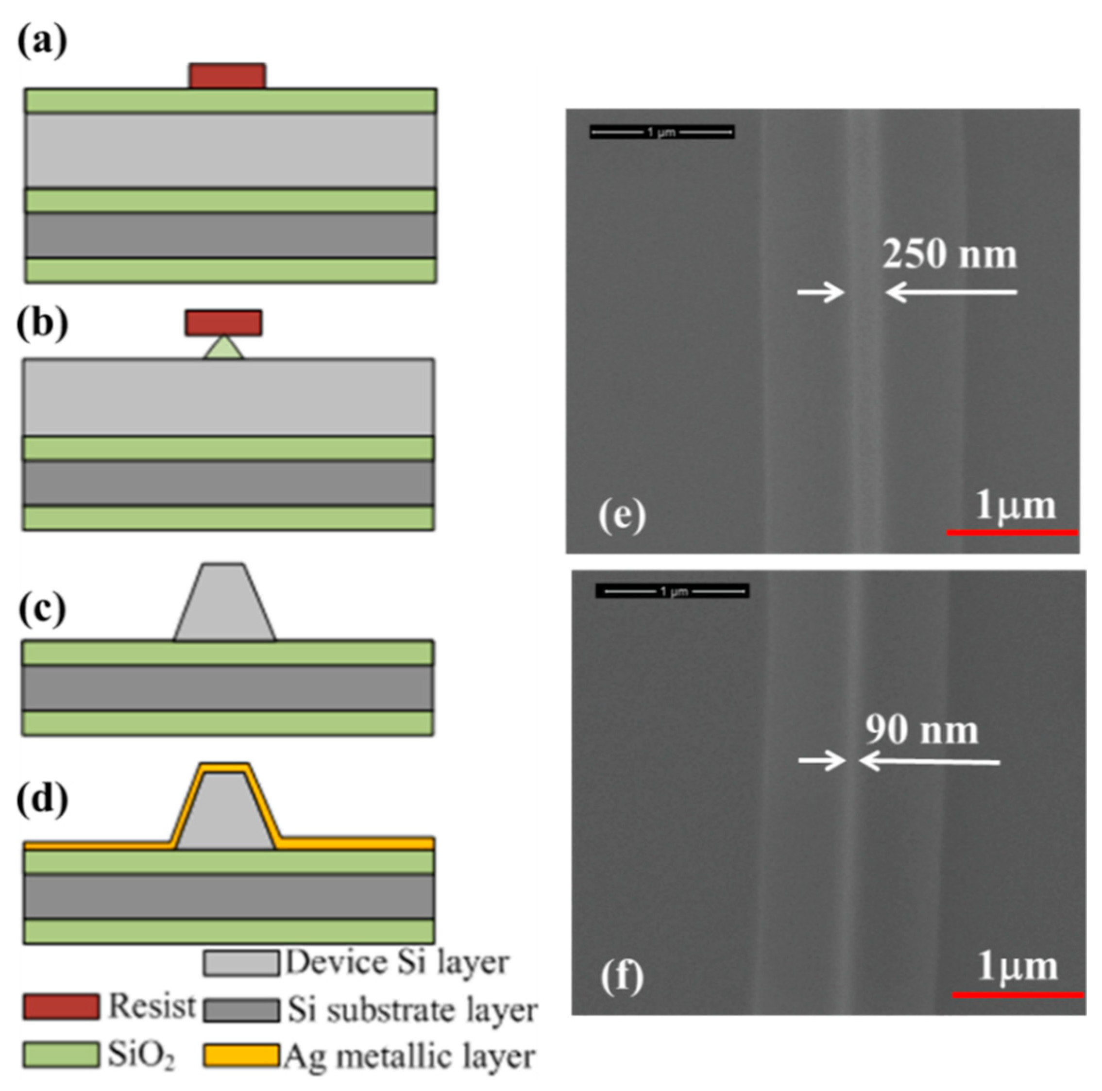
20]. In this work, the silicon waveguides are fabricated by wet–bulk micromachining using SOI wafer technology. The fabrication process is described in
Figure 2. By using conventional photolithography and the isotropic wet–etching of silicon dioxide in a buffered hydrofluoric acid (BHF) solution, we achieved SiO
2 mask nanolines to protect the silicon layer in the next etching steps (
Figure 2a,b). In the next step, the silicon waveguide is formed by the anisotropic wet–etching of single crystal silicon in a KOH solution (
Figure 2c). The sidewall of the silicon waveguide can be (100), (110) or (111) planes, depending on the etchant and crystalline orientation of the SiO
2 mask nanolines. Consequently, the silicon waveguide with the sidewall corner α can be 35.26°, 45°, 54.7° or 90°. The width of the top surface
w of the wedge SPP waveguide is controlled by calculating the under-etching time of the SiO
2 mask nanolines, and the height of the wedge SPP waveguide is determined by choosing the thickness of the device layer of the SOI wafer. The wedge SPP waveguides are completed by sputtering a thin Ag metal layer onto the fabricated silicon waveguide to form the metal/dielectric (Ag/air) interface.
Figure 2e,f show the field emission scanning electron microscope (FESEM) images of the fabricated silicon waveguides. The wedge SPP waveguides with the trapezoidal cross-section are fabricated from a (100) SOI wafer and anisotropic wet–etching of single crystal silicon in a KOH solution, so the sidewall corner is 54.7°. The height of the silicon waveguides
h is 1 μm, and the top surface width
w is 250 nm and 90 nm corresponding to the under-etching times of 2 min. and 6 min, respectively. The silicon waveguide with the triangular cross-section can be obtained by further decreasing the SiO
2 mask line at step 2(b).
In this research, we investigate the propagation characteristics of the WPP mode on the Ag/Air interface, concentrating on the two edges of the wedge SPP waveguides. The two edges of the metal layer are filleted with the same radius of 10 nm to keep the Ag layer thickness at a constant. In order to investigate the propagation characteristic of the surface plasmon wave on these wedge SPP waveguides, we use the finite element method. The boundary mode analysis problem in the COMSOL Multiphysics software is used to solve the propagation constant of the electromagnetic wave. The propagation characteristics of the wedge SPP waveguides are evaluated at the optical telecommunication wavelength of 1.55 μm. At this wavelength, the complex refractive index of Ag is 0.15649–11.567i. The refractive indexes of silicon and silicon dioxide are 3.4757 and 1.4957, respectively. The propagation characteristics of the wedge SPP waveguides are not affected by the waveguide material and silicon dioxide layer, which is explained by the fact that the SPP propagation is determined by the SPP waves propagating on the Ag/air interface. However, the thickness of the metallic layer must be carefully chosen in order to eliminate the coupling effect between the dielectric photonic modes and the WPP modes. For the flat interface between a metal and a dielectric, the penetration depth of the evanescent field into the dielectric, at which the field falls to 1/e, is determined by δ =
[
1], where
is the wave number in vacuum,
is the real part of the complex dielectric constant of metal, and
is the dielectric constant of the dielectric. For the wedge SPP waveguide structures with the non-flat metal/dielectric interface, we have used the finite element method to investigate the effect of the Ag film thickness on the SPP propagation characteristics. The investigated results show that when the Ag film thickness is larger than 200 nm, the propagation characteristics are almost unchanged. Therefore, the Ag film thickness is chosen to be 200 nm in the investigations.
On a metallic wedge, the WPP mode is the coupling mode formed by two SPP waves propagating toward the apex on the two opposite faces of the metallic wedge [
25]. The group velocity tends to zero, while the wave vector tends to infinity at the apex. This leads to an infinitesimal mode size (nanofocusing), and the wave can be propagated on a very large distance. However, this model is applied only to very small wedge angles (< 7°). For the larger wedge angles and complex waveguide structures, we use the numerical simulation method. In the simulation, a three-dimensional finite element model with the size of 4 × 4 × 10 µm
3 is used. Two numerical boundary ports are applied on the back and front faces of the wedge SPP waveguide to analyze the modes that can propagate in the waveguide structure. The direction of the propagation wave is along the x axis, as shown in
Figure 1. The perfectly matched layer is five times larger than the calculation domain. Because the electromagnetic fields concentrate mainly at the two wedges of the wedge SPP waveguides, the meshing is extremely fine in this area and coarser in other regions. The finest mesh is in the wedge region of the device shown by the red dashed rectangle in
Figure 1b. Because the model has a prismatic shape, we can use the swept mesh along the axis of the device, the x axis. We set two parameters in the meshing process, which are the number of swept elements
ns and the number of elements per wavelength in the cross-section
nm. The maximum size of the swept element is
l/
ns, where
l is the length of the device. The maximum size of the meshing element per wavelength is λ/(
n ×
nm), where n is the refractive index for the dielectric media and is the real part of the dielectric constant for the dispersive medium. In the simulation, we set
ns = 10 and
nm = 60, ensuring the convergence of the calculation. The smallest element size is about 1 nm at the wedge region of the device.
By solving the eigenvalue equations, we achieve the complex propagation constant β, before deriving the effective mode index (
neff =
Re(
Neff)) and propagation length
L = [2Im(β)]
−1. The normalized effective mode area (
Aeff/
A0) is calculated via the expression [
26]:
In Equation (1),
A0 (=λ
2/4) is the diffraction-limited mode area in free space. The electromagnetic energy density
W(
r) is defined as:
where
E(
r) and
H(
r) are the electric and magnetic fields,
ε(
r) is the electric permittivity and μ
0 is the vacuum magnetic permeability.
To evaluate and compare the performance of the wedge SPP waveguides, we use the figure of merit
FoM as the trade–off between the attenuation and the confinement, which is defined by [
27]
In the following sections, we will use the above parameters to evaluate and compare the performance of the wedge SPP waveguides.
3. Propagation Mode of Wedge SP Waveguides
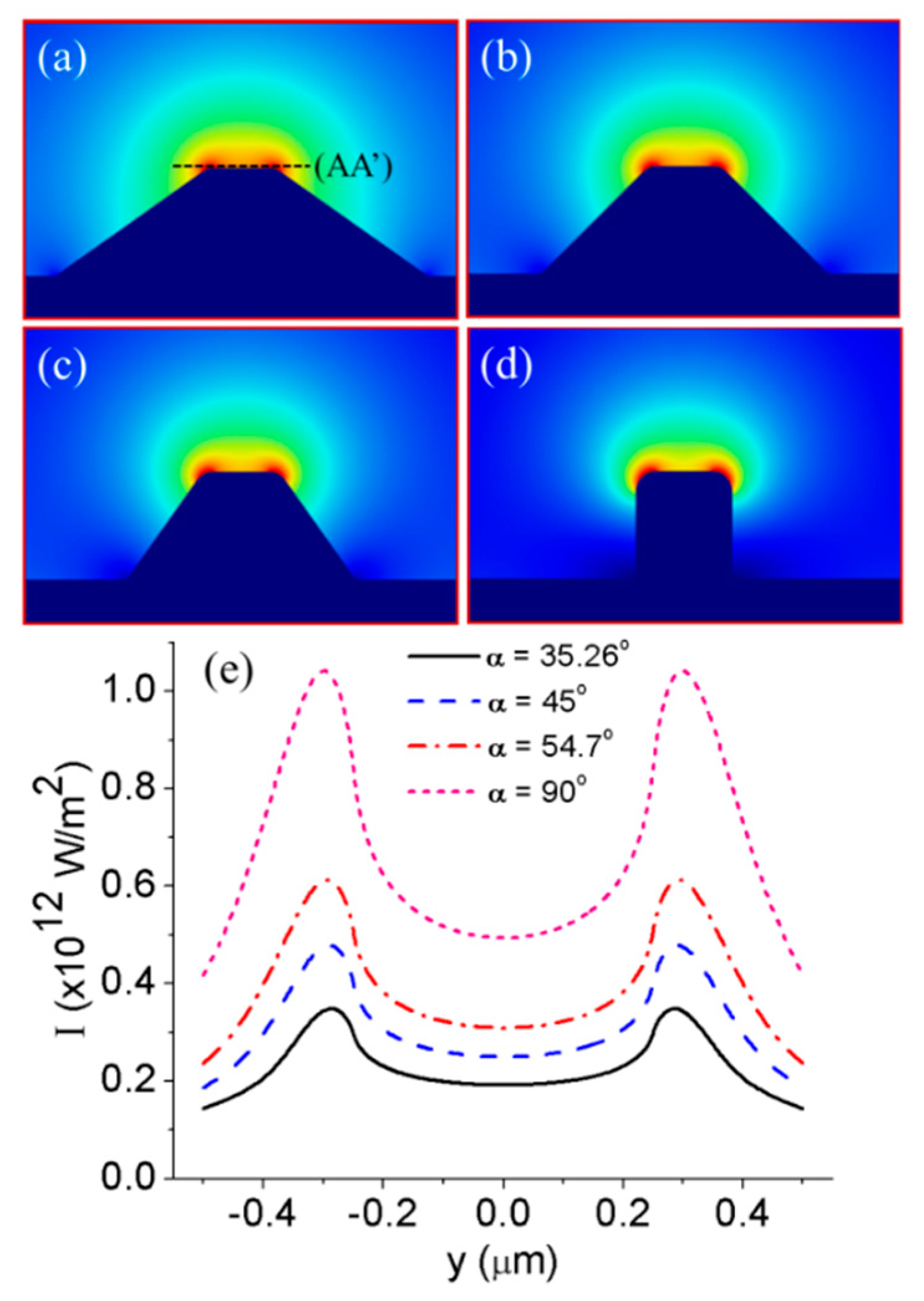
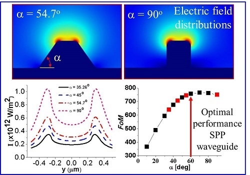
The distribution of the normalized electric field at various values of the sidewall corner α is shown in
Figure 3. As seen in
Figure 3a–d, the electric field concentrates mostly in the air medium, near the top surface of the wedge SPP waveguide structure for all cases. This result is similar to the WPP mode on the metal wedge (triangular-shaped SPP waveguides) that is described in previous research [
9,
25]. However, in the case of the trapezoidal–shaped SPP waveguide, there are two identical wedges which are located very close to each other. This leads to the an electromagnetic energy which is not only concentrated at two wedges but also spread on the top surface of the wedge SPP waveguide. To clarify this characteristic, we plot the distributions of light intensity along the AA’ cutline near the top surface of the wedge SPP waveguide structures, as shown in
Figure 3e. The light intensity reaches the maximum value at the two edges and the minimum value at the middle of the top surface. The input power is the same for every wedge SPP waveguide; however, the value of the light intensity is very different, which is due to the difference of confinement in each wedge SPP waveguide structure. When the sidewall corner increases, the light intensity increases because of the enhancement of the confinement.
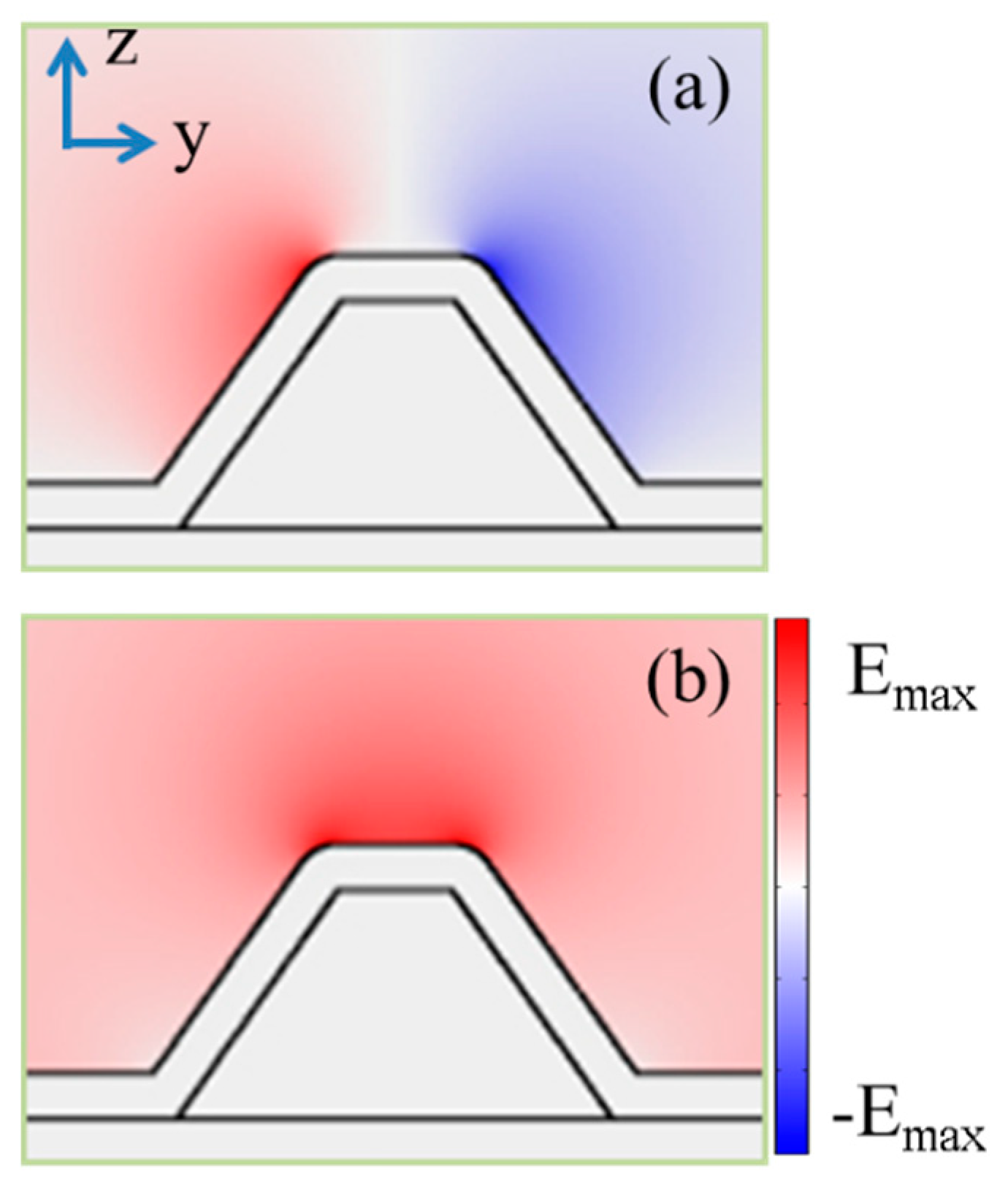
Figure 4a,b show the distribution of
Ey and
Ez electric field components for the case α = 45°, respectively. The
Ey electric field component shows an asymmetrical distribution on the two sidewalls, mainly at the two wedges, while the
Ez electric field component distributes symmetrically over the top surface of the waveguide. In the following section, we will focus on investigating the characteristics of this fundamental propagation mode of wedge SPP waveguides.
4. Modal Characteristics of Wedge SPP Waveguides
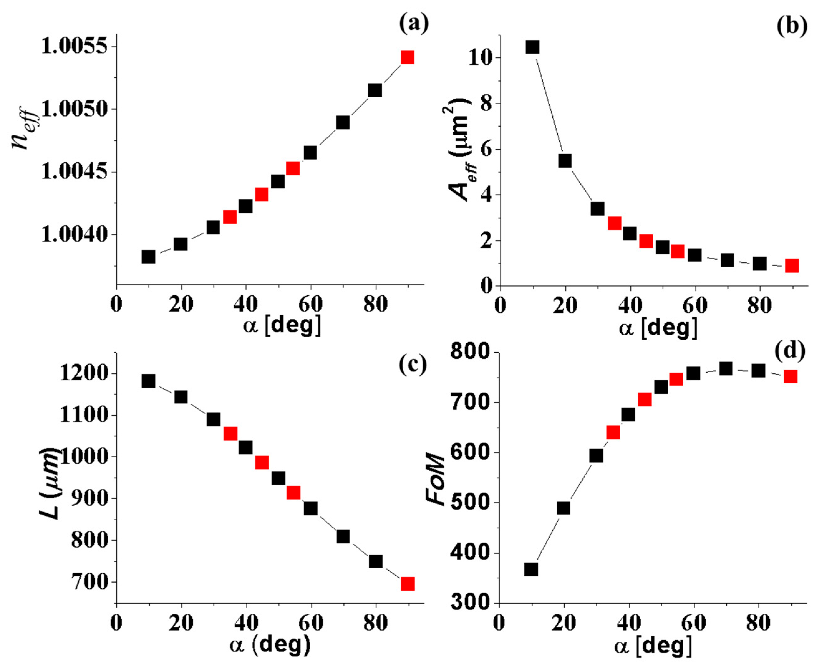
The four parameters of the propagation characteristic of the wedge SPP waveguides investigated as a function of the sidewall corner are shown in
Figure 5. When α increases, the effective mode index increases, while the mode area and propagation length decrease. This indicates that the mode confinement is enhanced at the cost of increased attenuation. For the trade–off between the confinement and the attenuation, we use the figure of merit
FoM, which is shown in
Figure 5d. In this investigation,
w and
h are fixed at 500 nm and 1 µm, respectively. At small values of α, the quality of the wedge SPP waveguide is low. The
FoM value increases when we increase the sidewall corner, obtaining a maximum value at around α = 60°. The red dots in these graphs correspond to the propagation characteristics of the wedge SPP waveguides, where the sidewall corner can be fabricated by the anisotropic wet–bulk micromachining of single crystal silicon. Thus, the wedge SPP waveguide with the sidewall corner α = 54.74°, which is usually fabricated by anisotropic wet-bulk micromachining of a (100) silicon wafer, almost achieves the best performance for a wedge SPP waveguide.
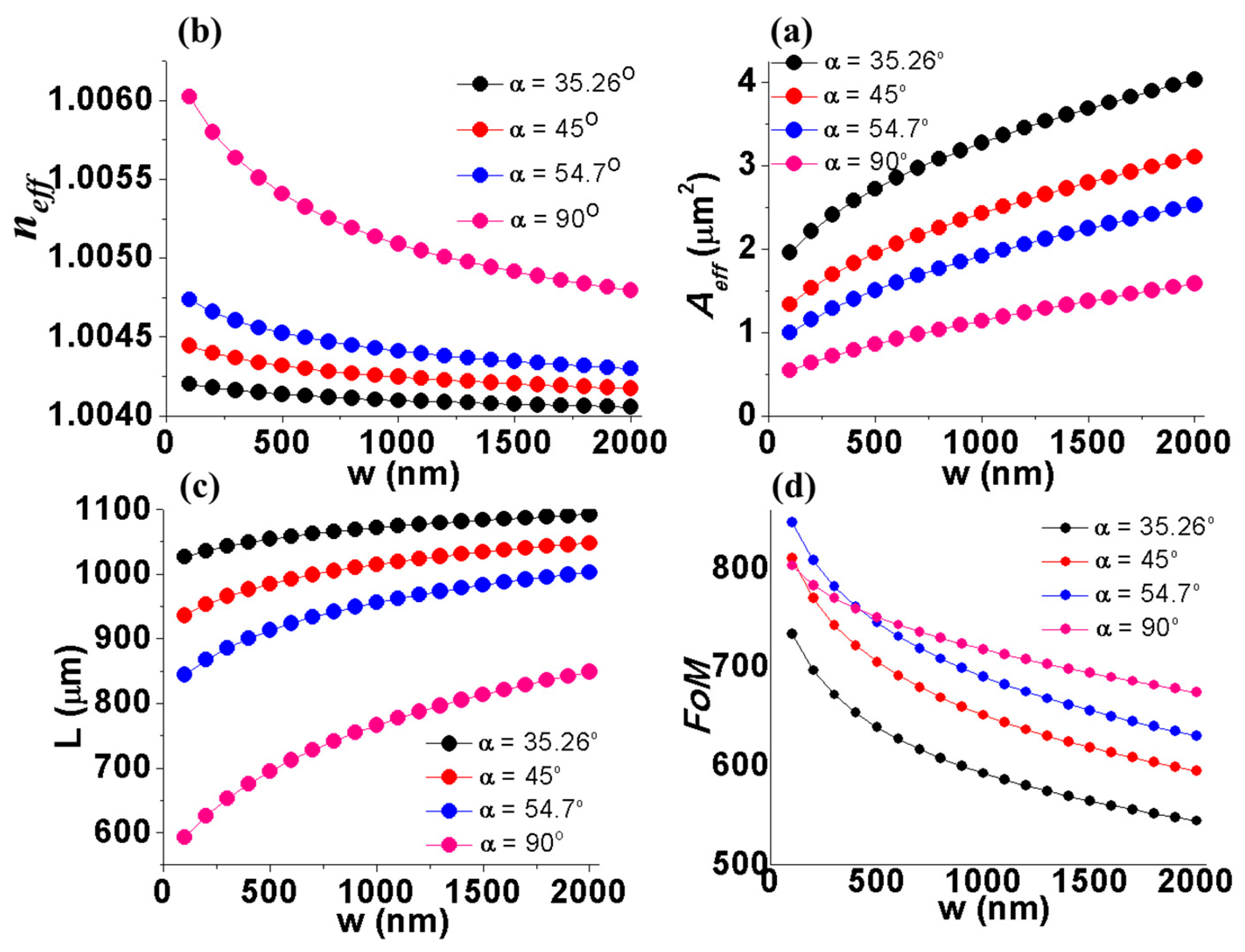
In the above investigation, the values of
w and
h are fixed at 500 nm and 1 µm, respectively. For a more comprehensive investigation, we study the dependence of propagation characteristics on the width of the top surface of the wedge SPP waveguides for the typical cases of the sidewall corner that can be fabricated by the anisotropic wet etching of single crystal silicon. The simulation results are shown in
Figure 6. The width of the top surface is investigated in the range from 100 nm to 2 µm with a step of 100 nm. As seen in
Figure 6a–c, when the value of
w increases, the effective mode index decreases, while the effective mode area and propagation length increase monotonically. The expansion of the mode size is due to the hybridization between the two WPP modes maintained at small
w values. When
w gets larger values, the two WPP modes become two independent propagation WPP modes, and the modal characteristics approach asymptotic behaviour. The modal characteristics rapidly approach asymptotic behaviour for the smaller values of the sidewall corner. The performance of the wedge SPP waveguide can be evaluated by the
FoM value, as shown in
Figure 6d. The
FoM value decreases monotonically with
w. Here, there is one critical value at
w = 400 nm. For the width of the top surface larger than 400 nm, the wedge SPP waveguide with the sidewall corner α = 90° shows the best performance. However, when
w is smaller than 400 nm, the wedge SPP waveguide with the sidewall corner α = 54.7° becomes superior compared to the three remaining wedge SPP waveguide structures.
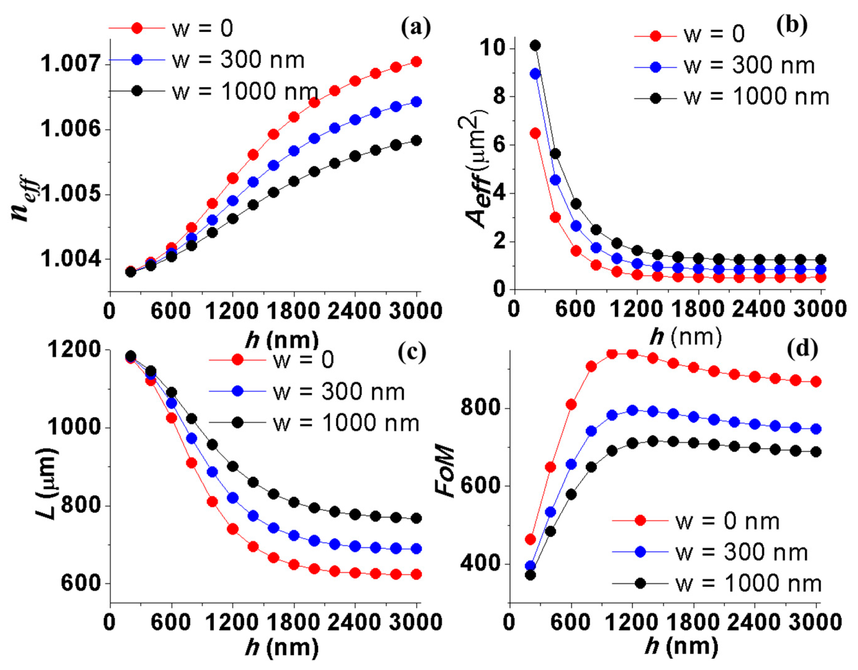
The next structure parameter of the wedge SPP waveguide that we consider here is its height. We choose the sidewall corner α = 54.7°, the width of the top surface
w = 0 nm, 300 nm and 1000 nm (
w = 0 nm is for the case of the triangular SPP waveguide). The influence of
h on the propagation characteristics is investigated in the range from 200 nm to 3 µm with a step of 200 nm.
Figure 7b,c shows a very fast decrement of the mode size and the propagation length when the height of the wedge SPP waveguide increases. The effective mode area approaches asymptotic behaviour at a smaller
h value (~1200 nm) compared to that of the effective mode index and propagation length. At very small
h values, the wave number of the WPP mode approximates the wave number of the SPP mode at the Ag/air interface, which leads to the SPP wave spreading on the metal surface; therefore, the mode area increases rapidly. From
Figure 7d, one can see that the wedge SPP waveguide with the best performance is at
w = 0 nm, i.e., the trapezoidal-shaped SPP waveguide becomes the triangular-shaped SPP waveguide.
Figure 7d also shows that the
FoM value obtains a maximum value which is at smaller
h values for the wedge SPP waveguides with smaller
w values.
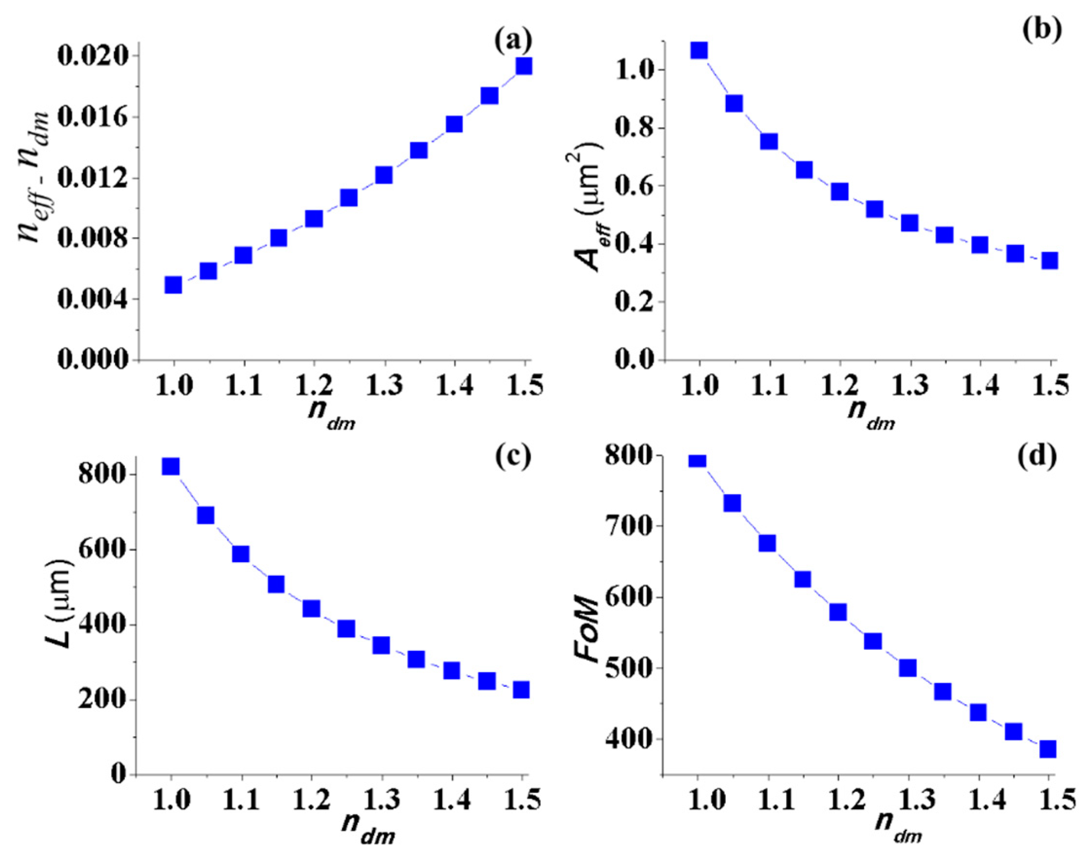
In the above investigations, we considered the wedge SPP waveguides embedded in air medium with a refractive index
nair = 1. If we change the embedded dielectric medium, the refractive index will become larger than 1, and the propagation characteristics of the WPP mode will be changed. Based on the above investigated results, we choose the structural parameters α = 54.7°,
w = 300 nm, and
h = 1 µm, before studying the dependence of the propagation characteristics on the refractive index of dielectric medium
ndm. These results are shown in
Figure 8. When
ndm increases, the effective mode index of the WPP mode is slightly larger than the refractive index of the dielectric medium. The difference of
neff and
ndm investigated as a function of
ndm is shown in
Figure 8a. When
ndm increases, the mode confinement is enhanced but the attenuation also increases rapidly (
Figure 8b,c).
Figure 8d shows that the dielectric medium with the low refractive index gives a wedge SPP waveguide with a better performance. The changed dielectric medium is also referred to in the case where the Ag film is oxidized. The silver oxide film does not support the SPP propagation, so the SPP propagation length of the device with the oxidized Ag film has decreased. To protect the Ag film from oxidization, a thin layer of silicon dioxide can be deposited on the surface of the Ag film. The Ag film can also be replaced by an alternative metal inert to media such as Au. Although the SPP propagation length of the device using the Au film has decreased, the propagation mode area is almost the same as that using the Ag film. Moreover, the air medium can also be replaced by active dielectric materials such as fluid or thermo-optic polymers [
28,
29]. Therefore, by tuning the refractive index of the fluid or the thermo-optic polymers, we can control the propagation characteristics of the WPP mode.

