Abstract
An ultrafast laser system combined with an optical delay line allowed ablation and in-scription at 1 kHz and 1 GHz pulse burst within transparent polyimide films. The two-photon-induced absorption results in clean surface ablation, while inscription results in polymer decomposition, creating carbonised regions within the polymer. Three pulse bursts at 1 GHz increased the observed coupling to the material significantly. Modified regions (with linewidths down to a few microns) were investigated using optical microscopy, white light interferometry, SEM and Raman spectroscopy, supporting the increasing carbon density relative to the pristine polymer. As depth of field was only a few microns at high NA, 3D micro-structuring was achieved. Polymer decomposition produces gaseous products, resulting in internal stress and thus affecting inscription fidelity. An inscribed subsurface electrode with dimensions of 5 mm × 0.3 mm × 3 μm connected to conducting vias had a resistance of R = 10.6 ± 0.2 kΩ, along with resistivity of ρ ~ 0.19 Ω cm; hence, it had DC conductivity, σ ~ 5.3 Scm−1. This conductivity is similar to that of bulk graphite and could well form the basis of future flexible sensors, demonstrating single-step 3D subsurface inscription of carbon or laser-induced graphene structures.
1. Introduction
This paper describes the use of femtosecond laser pulse burst to inscribe subsurface 3D carbon structures inside polyimide to create carbon electronic circuits and sensors. Polyimide is a high-performance thermoplastic that is currently used in a wide range of applications in flexible electronics, aerospace and automotive, due to its excellent physical properties, such as good dimensional stability, high mechanical strength, high radiation resistance, thermal stability, high dielectric strength, low thermal conductivity and transparency from 550 nm to >1 μm [1,2,3,4,5,6]. The study of laser material interactions on this polymer, whether for fundamental research or its modification for potential applications, is therefore of great interest.
In a review of functional PI films and micro-structures for flexible MEMS applications, the authors mentioned “laser-induced graphene” (LIG), a method to laser create carbon tracks by Direct Laser Write (DLW) using pyrolysis at λ = 10.6 μm, with CO2 lasers as the main route to surface laser patterning for printable electronics [7,8]. The surface temperature can exceed 2500 °C, converting the sp3 hybridised carbon atoms to sp2 and thus increasing conductivity. However, only surface micro-structuring can be achieved at MIR or UV wavelengths where there is a strong linear absorption coefficient [9,10,11,12].
On the other hand, at wavelengths where the polymer is transparent, femtosecond laser pulses are useful for both surface and internal micro-structuring, as peak electric fields exceeding E ~ 1013 Vcm−1 induce strong multi-photon absorption [13]. NIR femtosecond ultrafast ablation thresholds on polyimide are wavelength-, pulse-length- and pulse-number-dependent [14], increasing significantly at picosecond pulse length, accompanied by melt expulsion [15]. The importance of femtosecond pulse length in material modification, increasing NL absorption, is therefore critical.
A study of the non-linear (NL) interaction of 50 fs/800 nm pulses with 1.3 μm thick polyimide films on borosilicate glass produced highly controlled nano-blisters and confined chemical changes at the interface [16]. Threshold peak intensity for blister formation was I ~ 3 × 10¹² Wcm−2, while the primary interaction mechanism was regarded as NL three-photon absorption [17].
Fs laser applications on polyimide include high-throughput precision ablation of (negative master) microfluidic structures [12]; ultrafast laser 2D surface carbonisation (laser-induced graphene, LIG), followed by singulation, to produce 3D Kirigami-inspired strain sensors [18]; and ultrafast laser cutting of polyimide films on glass to singulate thin-film transistor (TFT) circuits [19]. An increase in surface hydrophobicity and a reduction in contact charge transfer were observed after surface micro-structuring PI with 800 nm/150 fs pulses and pulse overlap of 250 pulses per μm [20]. The resulting black surface showed clear D (disordered) and G (graphite) Raman bands at 1350 cm−1 and 1580 cm−1, corresponding to graphene and crystalline graphite, respectively.
Direct fs laser writing within the bulk of polyimide to create conductive graphitic carbon vias has been demonstrated, connecting Ag nanowires together and hence providing a technique for 3D fabrication of electronic circuits [21]. Typical via resistivity was observed to be ~6 Ωcm, while a threshold turn-on voltage was also required but reached 100% for exposures > 104 pulses/μm. Raman spectroscopy also confirmed clear D and G peaks at 1350 cm−1 and 1594 cm−1, respectively, expected for graphite within the vias. Using the same technique, this group used low-resistance conducting vias to connect encapsulated and randomly positioned LEDs, relevant to micro-electronic packaging [22].
As diamond is a pure form of carbon with bandgap Eb = 5.5 eV and radiation-hard, its conversion to graphitic carbon electrodes with holographic fs processing produced 3D detectors for high-energy-charged particles [23,24] with resistances down to 250 kOhm in p-CVD. However, many electrodes required a high DC voltage (~±100 V) to overcome a Schottky barrier, creating pure Ohmic conducting wires due to Joule heating.
While surface LIG offers an attractive method to incorporate graphene structures on polymers, integration into scalable electronics is hindered by complex, energy-intensive and toxic fabrication processes to encapsulate the micro-structures.
This paper demonstrates the ability to overcome these limitations by introducing fs DLW inside polyimide, inscribing 3D porous carbon tracks directly within the bulk polymer with both kHz and 1 GHz pulse bursts. In the latter case, improved uniformity of internal conducting electrodes is achieved, requiring no turn-on voltage, hence the first demonstration of fs pulse burst applied to internal polymer carbonisation. Within bulk, pulse bursts have been applied only to two-photon polymerisation in photo-sensitive liquid polymers [25,26].
Some relevant processing parameters on PI for generating conductive layers (surface and internal) are shown in Table 1. A primary aim of the current work, which is to match or exceed the DC conductivities shown, was achieved, reaching σ ~ 5.3 Scm−1 with the aid of 1 GHz pulse burst, created with an optical delay line.

Table 1.
Parameters for generating conducting layers on surface (Surf.) and internal (Int.) within polyimide.
2. Materials and Methods
A schematic diagram of the optical layout setup is shown in Figure 1. The output from an ultrafast Regenerative Amplifier (Clark-MXR CPA 2010, (Dexter, MI, USA), τ = 200 fs, λ = 775 nm, 1 kHz, 1 mJ, M2 = 1.2) was attenuated and directed to a pulse burst generator delay line. This consists of a half-wave plate (HWP1), Glan laser polariser (polarisation beam splitter, PBS), 3 dielectric reflecting mirrors and internal half-wave plate (HWP2) within the loop, creating a reflected |V⟩-polarised pulse, followed by a series of circulating pulses, termed pulse burst, with output |H⟩ polarised. This type of delay line, used with a 10 ps laser source, was briefly described by us previously [27]. As the optical path length within the delay line was ΔL = 30.0 ± 0.5 cm, the intra-burst frequency was νIB = 1000.0 ± 1.6 MHz. Up to three pulses with equal energy could be created, or a series of pulses with decaying amplitude up to n > 5 and overlapped in the near field. After traversing a periscope, the beam was expanded by a ×2 magnification telescope (L1 = 50 mm; L2 = 100 mm) with a fast shutter placed close to the focal plane of lens L1. A thin-film pick-off with a focus lens allowed observation of the burst spot pattern on a Spiricon CCD camera, and it was physically overlapped on the CCD by careful adjustment of the delay line mirrors. This procedure ensured that the pulse bursts were also overlapped at the focus of the 0.55 NA objective (Nikon CFI LU Plan Epi ELWD 50×, working distance = 10.1 mm, Castle Donington, UK).
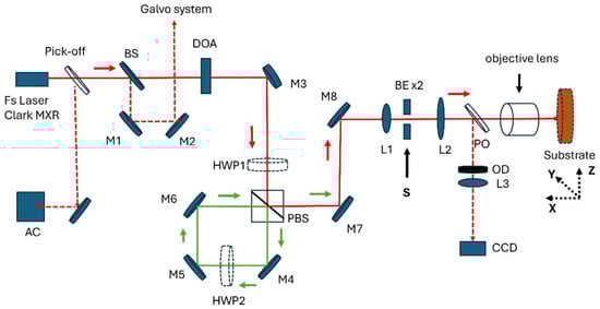
Figure 1.
Schematic of the optical setup. The output beam, attenuated by a diffractive optic attenuator (DOA) is reflected into the pulse burst delay line composed of HWP1, PBS, mirrors and HWP2. After traversing a periscope, the beam is expanded (×2), and a thin-film pick-off reflects a low-intensity component through OD filters to the Spyricon CCD, focused with a 200 mm focal length lens. The sample is mounted on a 3-axis motion control system, while a fast shutter, S, is synchronised to the controller. AC is an autocorrelator.
The polyimide samples (Kapton HN, Dupont, Contern, Luxembourg), 125 μm thick, approximately 12 × 12 mm) were clamped in a brass holder with an 8 mm clear aperture and mounted on a 1” mirror mount. A three-axis (X, Y, and Z) motion control system (Aerotech ATS-100, A3200, Reading, UK) adjusted the sample surface close to the focal plane. By observing the transmitted light through the PI film with an NIR camera, while carefully adjusting the sample along the optic axis, the front surface focal plane (X = XS) could be detected by a sudden drop in intensity due to surface ablation. The focus could then be placed at a given depth below the PI surface for internal inscription.
3. Results
3.1. Delay Line
A schematic diagram of the burst generator output is shown in Figure 2, with 1 kHz fundamental frequency and 1 GHz intra-burst frequency. The relative setting of HWP1 and HWP2 allows for the generation of two pulse burst (1, 1, 0), (|V⟩, |H⟩, 0) and three pulse burst with orthogonal polarisations (|V⟩, |H⟩, |H⟩) with nearly equal energy. Pulse bursts with n > 3 and varying amplitude can also be generated.
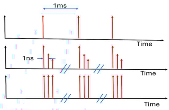
Figure 2.
Schematic of output pulse sequences from delay line with single-pulse (1, 0, 0), 1 kHz; triple-pulse burst (1, 1, 1) with decaying pulse energy; and triple-pulse burst (1, 1, 1) with equal energy. While the fundamental repetition rate is f0 = 1 kHz, the intra-pulse burst repetition rate is fb = 1 GHz.
Using a fast Photodiode (PD, Thorlabs DET025, Ely, UK) connected to a high-bandwidth digital oscilloscope (Tektronix MSO 5204, 2 GHz, Beaverton, OR, USA), we observed the temporal burst output after the Nikon objective with light scattered from a white card. Figure 3a–d show a range of pulse burst outputs observed on the fast PD when varying the relative positions of HWP1 and HWP2. These can decrease (a) or increase (b) with time, show a low-energy n = 2 pulse (c) or produce three nearly equal pulses (d) with low energy in higher n > 3 pulses.
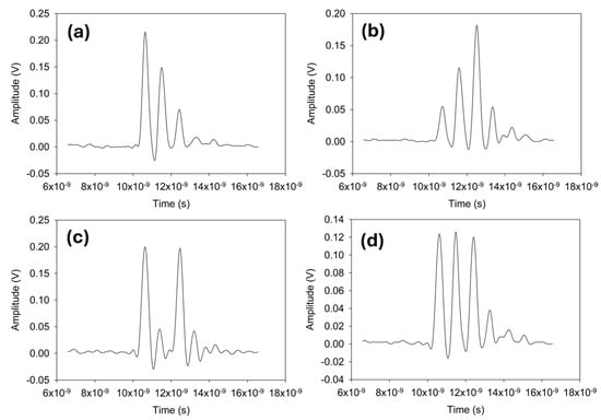
Figure 3.
A range of observed delay line pulse amplitudes when varying relative positions of HWP1 and HWP2: (a) decaying sequence of pulses, (b) increasing sequence followed by decay, (c) pulse burst with energy mainly in the first and third pulses (500 MHz), and (d) a triple-pulse burst with nearly equal energy. There always remains some energy in pulses for n > 3. Time base = 2 ns/division.
Although the observed pulse outputs can be appreciated from an optical perspective, it appears useful to calculate the expected relative pulse energies when polarisation directions are set beforehand. The Glan-laser polariser (polarisation beam splitter, PBS) transmission axis is set horizontally. Any component reflected from the PBS is vertically |V⟩-polarised, while any pulses transmitted through the PBS are horizontally |H⟩-polarised. This principle applies independent of beam direction through the PBS. If incident pulse energy is Ep, then for orientation of the electric vector, θ, at the polariser (orientation of fast axis θ/2), we get first reflected pulse energy, E1(V) = Ep sin2θ, and hence the transmitted component into the delay line, ETR(H) = Ep cos2θ. Setting HWP2 fast axis horizontal (φ = 0), maintaining |H⟩ polarisation within the delay line, the second pulse, transmitted through the PBS, is E2(H) = EpR3THWP cos2θ, where R is the mirror reflectivity and THWP is the transmission of the HWP2. If we assume that R ~ 0.99 ~ THWP2 and set θ = 45°, then E1(V) = 0.5 Ep, and E2 (H) = 0.48 Ep, close within 4%, and can be made equal with a slight adjustment of HWP1. This is a double-pulse burst (1, 1, 0), or (|V⟩, |H⟩, |0⟩), at 1 GHz intra-burst frequency. By adjusting the HWP2 so that the E vector within delay line is now rotated to angle φ at the PBS, the transmitted energy of the second pulse will instead be E2(H) = EpR3THWP cos2θ cos2φ. If the fast axis is set to φ/2 = π/4, then the circulating |H⟩-polarised pulse is rotated to |V⟩, (φ = π/2); hence, E2 (H) = 0, and the pulse is totally reflected back into the delay line, resulting in an n = 2 “dark pulse” with near zero energy. As this |V⟩-polarised pulse is again rotated by π/2 by HWP2 to |H⟩ and thus transmitted by the polariser; this creates a double pulse (|V⟩, |0⟩, |H⟩) at half the burst frequency, 500 MHz (close to settings of Figure 3c).
Calculating the energy of the third and subsequent pulses in the burst requires care, as these are derived from |V⟩-polarised pulses whereas the first pulse entering the delay line is |H⟩-polarised. The transmission through the PBS, previously proportional to the cos2φ term, needs to be replaced by cos2(π/2-φ) = sin2φ. Hence, E3(H) = EpR6T2HWPEpcos2θsin4φ, E4(H) = EpR9T3HWP cos2θ sin4φ cos2φ, E5(H) = EpR12T4HWP cos2θ sin4φ cos4φ, E6(H) = EpR15T5HWP cos2θ sin4φ cos6φ and so on. By generalising this procedure, we find for n ≥ 3,
which results in a series of |H⟩-polarised pulses, En(H) = f(θ,φ), with varying energy. For example, by setting θ = 30° and φ = 60°, we find energies E1(V) = 0.25 EP, E2(H) = 0.18 EP, E3(H) = 0.39 EP, E4(H) = 0.09 EP, and E5 = 0.02 EP; hence, we obtain a varying sequence with highest energy in E3(H). The sum allowing for optical losses. On the other hand, setting θ = 35.1° and φ = 45.4°, we get E1(V) = 0.33 EP, E2(H) = 0.30 EP, E3(H) = 0.16 Ep, E4(H) = 0.08 EP, and E5 = 0.04 EP; hence, the first two pulses have nearly equal energy, with a decaying sequence afterward. Having the flexibility to rotate both HWPs, the three-pulse burst (1, 1, 1), (|V⟩, |H⟩, |H⟩) can be made nearly equal, with fourth and subsequent pulses being relatively low in amplitude (Figure 3d). As the delay line loses scale with R(3n−3) THWP(n−1), this attenuating factor becomes increasingly important as the pulse burst number, n, increases. For n = 4 and n = 5, this factor = 0.89 and 0.85, respectively.
En(H) = EPR(3n−3) THWP(n−1) cos2θ sin4φ cos(2n−6)(φ)
3.2. PI Film Surface Finish and Transmission
The Kapton film, when viewed under reflected light, appeared to have a better surface finish on one side. This was confirmed by measuring surface flatness using white light interferometry (Veeco Wyko NT1100, Chicago, IL, USA), a 3D surface profiler with transverse resolution ~0.5 μm in x and y, while z vertical resolution is ~1 nm. With five measurements (×50) front and rear, we obtained average and root mean square roughness, <Raf> = 18.2 ± 2.4 nm and <Rqf> = 35.7 ± 8.5 nm, while for the rear surface, we obtained <Rar> = 39.9 ± 3.7 nm and <Rqr> = 56.0 ± 8.5 nm, which are significantly higher measurements. Consequently, the surface with the lowest roughness always faced the laser beam to minimise scatter and focal spot distortion. The sampled area here was 123 μm × 100 μm.
The linear transmission of the film was checked with a collimated beam at λ = 775 nm and low fs pulse energy, yielding T775 = 0.56 ± 0.02; hence, the linear absorption coefficient was α775 = 46.4 ± 2.9 cm−1. With nanosecond pulses from the regenerative amplifier unseeded, this was found to be unchanged. This low linear absorption coefficient infers that multi-photon absorption (MPA) will be required for precise material modification.
3.3. PI Micro-Structuring, 0.05 NA
Material ablation was first investigated with the aid of a Galvo scanner (Nutfield), a 100 mm f-theta lens and Scan software (SCAPS GmbH, Samlight 3.5, Oberhaching, Germany). A series of tracks were machined while varying the pulse energy, Ep. Scan speed was s = 5 mm/s, with five overscans. Samples, which were mounted on a glass slide, were carefully brought to the lens focal plane on a four-axis micro-positioning stage, Aerotech Npaq (x, y, z, and θ). Effective NA = 0.05, with a focal spot size of D = (1.22 λ/NA)M2 = 22.7 μm; hence, the total pulse overlap is NT ~ 25 pulses/spot diameter. Figure 4a,b shows typical 3D surface profiles of scanned lines at Ep = 8.3 μJ and (fluence) F = 4.1 J cm−2, and EP = 19.5 μJ and F = 9.6 J cm−2, respectively, highlighting increased width and depth with fluence. The calculated ablation volume/mm of track in Figure 4c shows a weak quadratic dependence, while the ablation efficiency, or Specific Removal Rate (SRR), is shown in Figure 4d. This is defined as (V/nEp), the ablated volume per mm length divided by the total number of incident pulses of energy, Ep. This rises rapidly above threshold and then decays slowly, yielding <(V/nEP)> ~ 10 μm3/μJ. Threshold ablation energy is Eth ~ 0.8 μJ, (Fth ~ 0.4 Jcm−2), while ablation depth is d ~ 0.3 μm/pulse, with EP = 13.7 μJ. If d = α−1 Ln(Ep/Eth), then the absorption coefficient is α = α0 + βI = 9.5 × 104 cm−1 ~ βI, inferring that the two-photon absorption coefficient (2PA) is β ~ 2.9 cmGW−1 at peak intensity I ~ 3.3 × 10¹³ W cm−2. This may be typical of two-photon absorption coefficients in transparent, undoped polymers at such high intensity, where sequential photon absorption may lead to higher levels in the band structure following two-photon absorption [28]. In [28], the two-photon absorption coefficient converged in amorphous PolyEther (Ether) Ketone (PEEK) to β ~ 4.0 cm GW−1, with a peak intensity of I > 160 GW cm−2, while in [17], the 2PA coefficient for polyimide was assumed to be β ~ 1 cm GW−1, as the bandgap was similar to that of ZnO, and the 2PA coefficient for undoped polyimide was not reported.
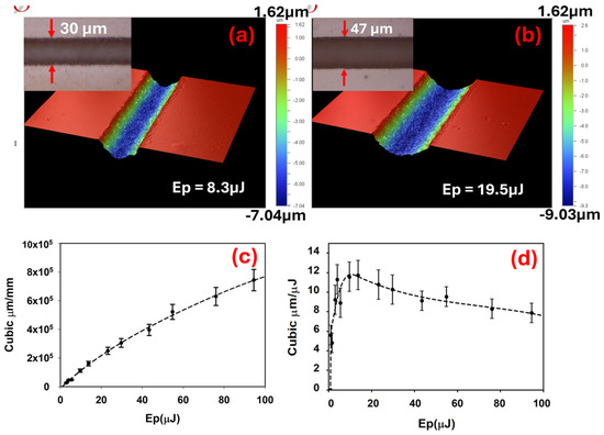
Figure 4.
Low-NA ultrafast laser ablation of PI film at 775 nm, line scans, 5 mm/s scan speed, 5 overscans: (a) Wyko 3D cross-section at EP = 8.3 μJ, insert, surface optical image; (b) Wyko 3D cross-section at EP = 19.5 μJ, insert, surface optical image; (c) ablation volume/mm length, with quadratic fit, error bars ± 1σ; and (d) ablation efficiency, which varies in the range of 5–12 μm3/μJ, with weighted smoothing spline (least-squares) fit. As expected, ablation efficiency approaches zero as Ep → Eth.
A comparison of single-pulse/multi-pulse ultrafast laser ablation thresholds of polyimide is shown in Table 2, showing that due to incubation, multi-pulse thresholds reduce while increasing pulse length to 7 ps, and single-pulse ablation threshold increases significantly.
Table 2.
Single- and multi-pulse (mp) ablation thresholds measured on polyimide.
3.4. PI Micro-Structuring, 0.15 NA
PI inscription was first attempted using a 0.15 NA refractive objective (Nikon, LU Plan ×5, WD = 18 mm, Castle Donington, UK) with a depth of field 12.2 μm. However, this was found to be unviable, and only surface ablation could be observed. Figure 5a–c shows optical images of an ablated surface pattern when scanning the film at a speed of s = 0.5 mm/s, with incident pulse energy of Ep = 3.7 μJ/pulse and line pitch of Λ = 50 μm. The resulting micro-structure showed some material re-deposition but little evidence of melting. This supports NL absorption as the primary ablation mechanism, likely two-photon at 775 nm where 2 hν = 3.2 eV > Eb ~ 2.3 eV [21]. The focal spot size here D = (1.22λ/NA)M2 ~ 7.6 μm with pulse overlap N = 15.2/spot diameter and fluence F = 8.2 Jcm−2. There is likely some carbonisation during ablation but darkening is mainly due to light scatter from the roughened, ablated surface while re-deposition appears minimal.
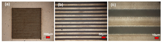
Figure 5.
Optical images of PI surface ablation with 0.15 NA focus objective, Ep = 3.7 μJ, scan speed at s = 0.5 mm/s, and line spacing at Λ = 50 μm, pulse overlap at N = 15.2, and fluence at F = 8.2 J cm−2: (a) low-magnification image of 2 mm square grating micro-structure, (b) higher magnification of ablated lines, and (c) highest magnification image highlighting clean ablation with limited debris re-deposition. Ablation rate is approximately 7.5 × 104 μm3/s.
3.5. Inscription, 0.55 NA, 1 kHz
With a higher, 0.55 NA, objective (Nikon LU Plan, ×50 EPI), internal inscription was achieved without surface ablation due to the tight focusing and hence limited depth of field, keeping surface fluence below ablation threshold. A grating structure with a pitch of Λ = 20 μm was scanned at a speed of s = 1 mm/s and pulse energy of Ep = 0.15 μJ. The expected focal spot size with 0.55 NA at 775 nm is D0.55 ~ 2.1 μm; hence, the modification fluence is F = 8.6 J cm−2, the pulse overlap is N = 2 and the peak intensity at focus is I ~ 2.2 × 10¹³ W cm−2. After inscription, the substrate was sectioned, mounted in clear epoxy and then optically polished to expose the modifications. Figure 6a shows an optical an image of both surface and internal modification, 40 μm below front surface. In Figure 6b, two gratings inscribed at depths of approximately 40 μm and 60 μm are observed, highlighting the 3D writing capability at higher NA.
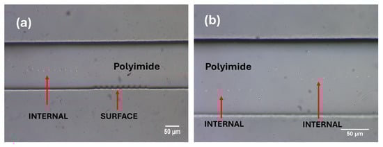
Figure 6.
Optical cross-sections of polished polyimide film after 0.55 NA inscription, E = 0.15 μJ, s = 1 mm/s, 20 μm pitch: (a) surface and internal modification 50 μm below, and (b) internal modification at 40 μm and 60 μm.
The inscription in Figure 6a,b appears to show light-guiding regions so that material modification likely resembles refractive index (RI) changes due to limited bond breaking at low-pulse overlap. These results indicate that exposure for material carbonisation needed to be higher—for example, by reducing scan speed/increasing pulse energy.
Figure 7a,b shows optical images (reflection/transmission) of surface and internal inscription at varying depths, from 40 μm to 80 μm, with increased energy, E = 0.3 μJ/pulse, and a reduced scan speed, s = 0.5 mm/s. The modified regions now appear wider, 5–10 μm.
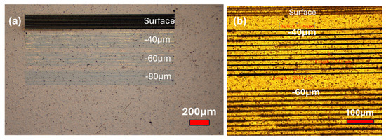
Figure 7.
Optical images of surface and inscribed gratings at 1 kHz with pitch Λ = 20 μm, EP = 0.3 μJ/pulse, and scan speed s = 0.5 mm/s: (a) reflection image, surface and internal inscription at varying depths; and (b) transmission image of filaments, 40 μm and 60 μm below surface.
3.6. Pulse Burst Processing, Stainless Steel
With the delay line carefully adjusted and spots overlapped on the Spyricon camera, a simple test of the delay line was accomplished by comparing the ablation of a polished stainless-steel sample at 1 kHz and 1 GHz. Scan speed was set to s = 0.5 mm/s and E = 0.15 μJ/pulse (F = 8.6 J cm−2). Figure 8a shows an optical image of line scans with 10 μm pitch at 1 kHz and 1 GHz, three-pulse burst. The 1 kHz ablation is clean, with a 2–3 μm line width and ~1 μm depth, while ablation with burst processing results in much stronger laser–material coupling with surface oxidation. Figure 8b shows a WYKO surface scan of both regions, with the GHz showing burrs ~1.5 μm high, and 2 μm ablation depth. The burrs are indicative of significant thermal effects during pulse burst processing at 1 GHz due to plasma absorption, resulting in melt expulsion. These results indicate that the delay line is aligned satisfactorily, and bursts are spatially overlapped.
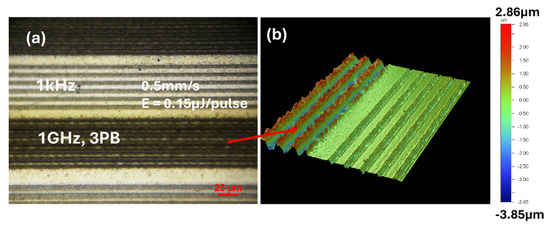
Figure 8.
Ablation at 1 kHz and 1 GHz (3PB) on stainless steel, s = 0.5 mm/s, E = 0.15 μJ/pulse: (a) optical image, highlighting increased thermal effects at 1 GHz; and (b) 3D Wyko image of surface profile, clean at 1 kHz, while pulse burst with plasma absorption results in melt expulsion, creating burrs at 1 GHz.
3.7. Pulse Burst Processing of PI, 1 GHz Intra-Burst
The use of the delay line was next investigated with the PI film. Figure 9 shows optical images in reflection (a) and transmission (b) of the internal inscription at 1 kHz and 1 GHz (three-pulse burst), respectively, with similar energy/pulse, E = 0.17 μJ, and scan speed, s = 0.5 mm/s. Here, one can observe a significant increase in the material modification (darkening) with pulse burst at 1 GHz relative to 1 kHz. In reflection, a yellow colouring appears around filaments that may well be due to internal stress generated by escaping gases after polymer decomposition.
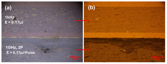
Figure 9.
Optical images of gratings inscribed 30 μm below PI surface with 1 kHz and 3-pulse burst 1 GHz, 0.5 mm/s: (a) reflection, 1 kHz, E = 0.17 μJ/pulse; and (b) transmission, 1 kHz and 1 GHz, 3-pulse burst, E = 0.17 μJ/pulse.
To create continuously modified regions (which could be regarded as internal electrodes), the scan speed was reduced to s = 0.2 mm/s, pulse overlap N = 10.5, while the line offset was reduced to Λ = 2 μm, close to the focal spot size. Figure 10 shows optical images of the resulting modifications (both surface and internal). Figure 10a shows surface ablation at 1 kHz with varying energy, along with internal inscription at 1 GHz (three-pulse, (1, 1, 1), ET = 0.45 μJ) and 1 kHz, EP = 0.15 μJ/pulse, observed in reflection. Figure 10b shows the same region, but in transmitted light, where there is significant light absorption, likely due to material carbonisation. The inscription depth is d = 50 μm. Figure 10c shows the 1 kHz modification with non-uniform darkening. On the other hand, the 1 GHz inscription, as shown in Figure 10d, is more uniform with increased exposure.
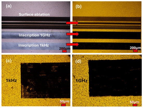
Figure 10.
Surface and internal modification of PI film at 1 kHz and 1 GHz pulse burst, 0.55 NA. Scan speed s = 0.2 mm/s, line separation Λ = 2 μm, Ep = 0.15 μJ/pulse, fluence F = 4.3 J cm−2, and focus 50 μm below surface: (a) low-magnification optical image in reflected light; (b) same regions observed in transmitted light; (c) 1 kHz, higher magnification in transmission, showing some non-uniformity of carbonisation; and (d) 1 GHz, (3-pulse) burst in transmission, showing more uniform modification.
The continuously processed regions were singulated with ultrafast pulses using the galvo system and 100 mm f-theta lens. These were then coated with approximately 20 nm of gold and imaged using SEM (Zeiss Gemini SEM 450, Cambourne, UK, Figure 11). Figure 11a shows the continuously inscribed region, approximately 50 μm below the surface, with 3-pulse burst at 1 GHz, where a slight curvature is apparent. Figure 11b shows a 1 kHz inscription, where unexpected jumps in the focal plane are observed, the source of which is not yet clear. Figure 11c shows the 1 GHz inscription at high magnification, while the electrode width is <0.5 μm. A faint ghost beam inscription also appears below, possibly due to spherical aberration at the air/polymer interface at 0.55 NA. Figure 11d shows the surface ablation cross-section at high magnification.
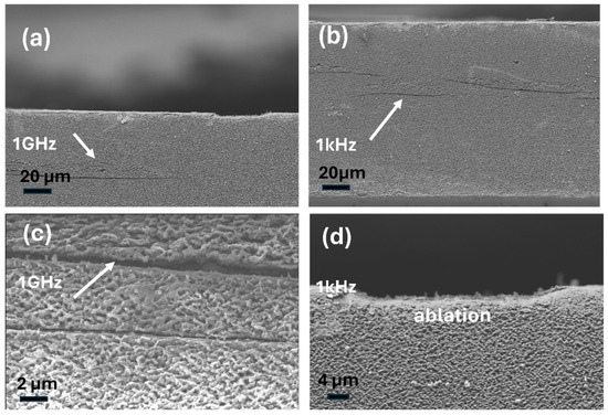
Figure 11.
SEM cross-section images of singulated PI sample, surface and internal inscription, s = 0.2 mm/s, E = 0.15 μJ/pulse: (a) 1 GHz (3PB) continuous pad 50 μm below surface, where slight curvature is evident; (b) 1 kHz inscription a same depth, where unexpected jumps in the focal plane > 10 μm are observed during inscription; (c) high-magnification image of 1 GHz pad, showing modified layer has width w < 0.5 μm, while effect of a weak ghost beam appears below; and (d) surface profile of 1 kHz ablated region with 2 μm offsets.
The ability to inscribe from the rear to front surface was tested by translating the focal spot through the PI film (rear surface first) in arrays with 20 μm spot separations and an initial translation speed of 1 mm/s, with pulse energy at E = 0.2 μJ at 1 kHz. A fast shutter (Thorlabs SH05, Ely, UK) was controlled through the Aerotech 3200 software, V4.08.001. Figure 12a shows an optical image of 10 × 10 spot arrays in transmission, while Figure 12b shows an optical cross-section after mounting the sample in clear epoxy and polishing down one axis. It is clear that the filaments (<3 μm width) show variable width and coupling to the material during inscription. Polishing precisely through the array Y-axis was difficult and may explain the appearance of the diminishing cross-sections outside the central two. The modification here along the optic axis at 1 mm/s may also indicate refractive index change and little carbonisation.
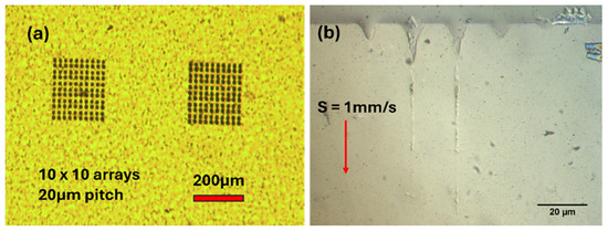
Figure 12.
Optical images of inscription of 10 × 10 arrays along the optic axis through the PI film, s = 1 mm/s, E = 0.2 μJ/pulse, 1 kHz: (a) in transmission and (b) polished cross-section of modifications where polishing axis is not exactly parallel to array Y-axis. The front surface is ablated as expected.
As carbonisation appeared very limited, as shown in Figure 12, scan speed was reduced by two orders of magnitude to s = 10 μm/s, corresponding to 100 pulses/μm. Pulse energy was EP = 0.15 μJ at 1 kHz, and total energy was ET = 0.45 μJ at 1 GHz, three-pulse burst. Array spacing was set at 100 μm. Figure 13 shows optical images of 1 kHz (a,b) and 1 GHz (c,d) front and rear surface modifications. The front surface at 1 kHz, as expected, shows similar surface ablation spots (~15 μm wide), while the rear modification is highly variable, with dimensions much reduced due to limited coupling and residual spherical aberration. At 1 GHz, the burst processing on the front surface is ~25 μm wide, while rear surface modification is much closer in dimension—however, rear surface variations between spots are still evident. Nevertheless, pulse burst gives more consistent results, and the material here looks carbonised. Interesting yellow ring structures appear around the spots at 1 GHz and may well be due to shock waves from laser–plasma absorption during pulse burst processing at pulse delays of 1 ns. Plasma expansion during ultrafast laser ablation typically occurs on the ns timescale [29].
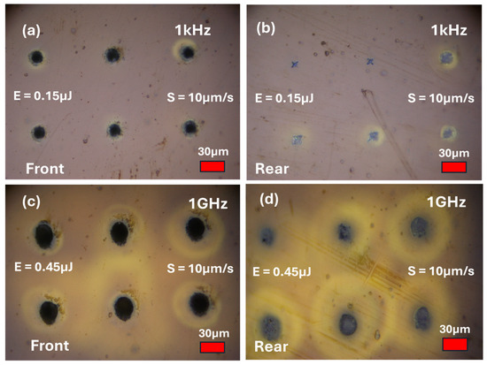
Figure 13.
Optical images of filaments drawn through the polyimide film from rear to front surface at speed s = 10 μm/s: (a) 1 kHz front surface ablation; (b) 1 kHz rear surface modification, highlighting large variations; (c) 1 GHz front surface ablation, showing effects of increased exposure; and (d) 1 GHz burst modification, highlighting more uniform micro-structuring and possible effect of shock wave effects due to plasma absorption.
In order to create thicker regions of carbonised PI, the substrate was scanned with Λ = 2 μm lines and δ = 1 μm offsets along the optic axis inside the film with 15 layers, creating continuously 3D-modified regions. Scan speed was set at 0.2 mm/s, and E = 0.15 μJ/pulse. Figure 14a shows an optical image of four scanned regions (1–4: 1 kHz, 1 GHz, 1 kHz, and 1 kHz) that are then singulated with the Galvo system. Figure 14b shows an optical image of the sectioned polyimide film. Modified regions are primarily at 50 μm depth; however, material-darkening also appears below the selected depth, constituting a significant fraction of the film thickness, especially at 1 GHz. Expected thickness here was 15 μm, while film-modification depth is more extensive, around 80 μm at 1 kHz and approaching 100 μm at 1 GHz. The source of these variations may be film mechanical distortion during inscription via material decomposition, producing gases such as CO, HCN, C2H2 and CO2 [30], thereby causing internal pressure and resulting stress. This may alter the effective focal plane during material exposure. The yellow colouration around inscribed regions, as seen in Figure 14a, is likely evidence of this decomposition.
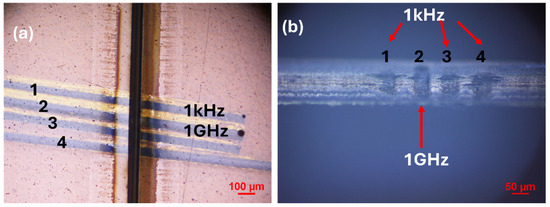
Figure 14.
Optical images of 3D inscription in polyimide at 1 kHz and 1 GHz pulse burst, s = 0.2 mm/s, 15 layers, 1 μm offsets: (a) reflection image after polyimide film singulation, showing colouration; and (b) cross-section of 3D modifications, highlighting inscription depths are much greater than expected.
3.8. Raman Spectra
The filamentary modifications at the rear face in Figure 13d with 1 GHz burst exposure were scanned using Photo Luminescence (PL) and Raman spectroscopy to detect any changes in molecular bonds after exposure. The system employed was a Horiba Jobin Yvon LabRAM HR800 UV confocal Raman microscope, excitation wavelength = 514 nm, objective = ×50/0.55 NA long working distance, confocal hole = 10 μm with Spectrometer grating = 1200 L/mm and Andor peltier cooled CCD. For PL, exposure time (for each segment of the spectra) = 30 s, acquisitions = ×5, and sub-pixel number = 5. Meanwhile, for Raman spectra, exposure time (for each segment of the spectra) = 80 s, acquisitions = ×5, and sub-pixel number = 5.
Data were collected at the centre of one of the laser-generated filaments, and for comparison, on the pristine, unexposed material. While a high level of fluorescence background is observed in the pristine material (Figure 15a), the treated material in the filament showed a significant suppression of fluorescence by >2 orders of magnitude throughout the wavelength range of 525 nm–750 nm. Figure 15b shows Raman spectrum, where the pristine polyimide exhibits two clear Raman peaks near 1401 cm−1 and 1609 cm−1, attributed to aromatic ring C–C stretching/imide-related vibrational modes and aromatic C=C stretching vibrations, respectively. A very broad feature above ~3000 cm−1 (FWHM ≈ 1000 cm−1) is also observed, associated with O–H and C–H stretching modes arising from adsorbed moisture and polymer functional groups. After laser exposure, the Raman spectrum is strongly attenuated across the entire wavenumber range, indicating substantial alteration of the polymer structure. No resolvable Raman bands corresponding to graphitic carbon (D, G, or 2D bands) are observed under 514 nm excitation at this exposure level (200 pulses/μm). Figure 15c,d shows the fluorescence and Raman signals on an expanded scale, respectively, where the Raman signals near 1401 cm−1 and 1609 cm−1 appear to be much reduced with regard to intensity.
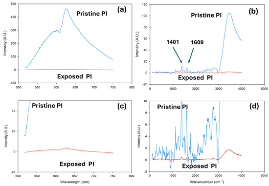
Figure 15.
Fluorescence and Raman spectra observed on polyimide with 514 nm excitation: (a) fluorescence scan of pristine region (blue) and exposed region (red) on the rear surface on centre of drawn filament (Figure 13d), and (b) Raman shift of pristine and exposed filament on wavenumber scale. The fluorescence and Raman peaks near 1401 cm−1 and 1609 cm−1 have almost completely disappeared after laser exposure: (c) fluorescence on expanded scale, and (d) Raman signal on expanded scale, now showing the peaks near 1401 cm−1 and 1609 cm−1, much reduced in intensity.
Raman spectroscopy at 514 nm is highly susceptible to fluorescence and absorption effects in laser-modified polyimide; therefore, the absence of resolvable D/G bands does not exclude the presence of disordered sp2-rich carbon [31].
3.9. Electrical Measurements
A continuous electrode with dimensions of 5 mm × 0.3 mm × 3 μm (three layers, 1 μm separation) at 1 GHz (3PB) was inscribed 60 μm below the surface, with total pulse energy of ET = 0.45 μJ and a scan speed of s1 = 200 μm/s. A series of conducting vias (5 off, 25 μm separation) were then drawn from the last layer to the surface near each end using a much lower scan speed, s2 = 1 μm/s, connecting the electrode from the modified region to the PI surface. This micro-structure took >3 h to fabricate. Finally, Ag DAG (Acheson Electrodag 1415, Agar Scientific, Rotherham, UK) was brushed onto the ends of the structure, and the resistance was measured with a digital multi-meter. Figure 16a shows the LHS of the inscribed subsurface electrode with conducting vias reaching the surface. Figure 16b shows a photo of the single electrode with Ag DAG contacts. The resistance was measured to be R = 10.6 ± 0.2 kΩ, independent of polarity. We then inscribed two such electrodes, spaced by 1 mm with conducting vias and Ag DAG contacts (Figure 16c), with measured resistance of R = 5.5 ± 0.1 kΩ, approximately that expected for two electrodes in parallel.
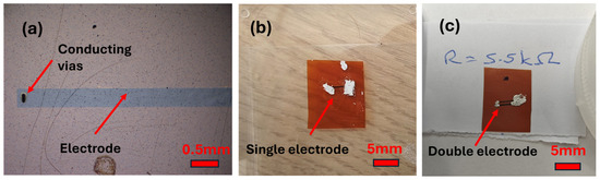
Figure 16.
Inscribed conducting electrodes with 1 GHz, 3-pulse burst, 60 μm below surface with dimensions 5 × 0.3 × 0.003 mm: (a) optical image of the continuous subsurface electrode with conducting vias brought out to the surface, lefthand side; (b) photo of single electrode sample with the Ag DAG contacts; and (c) photo of double electrode with Ag DAG contacts.
If we assume an electrode cross-sectional area of A ~ 3 μm × 300 μm, (A ~ 9 × 10⁻⁶ cm2), then we can estimate the resistivity, ρ, of the inscribed electrodes (with vias). If resistance is R = ρL/A, where L is the electrode length (0.5 cm) and A is the area of the electrode cross-section, then resistivity can be estimated (assuming R = 10.6 × 10³ Ω) to be ρ ̴ 0.19 Ωcm. The DC electrical conductivity is σ = 1/ρ ~ 5.2 Scm−1. This electrical conductivity is typical of through-plane bulk graphite, 1–100 Scm−1, whereas the conductivity along the layers (graphene) has S ~ 103 Scm−1 [32]. We have Ohmic behaviour of the internal electrodes, not requiring a turn-on voltage—at least not >9 Volt.
4. Discussion and Conclusions
Ultrafast micro-structuring has been demonstrated on polyimide films, resulting in clean surface ablation due to ultrahigh-intensity-induced two-photon absorption at λ = 775 nm, with the two-photon absorption coefficient estimated to be β775 ~ 2.9 cm GW−1 at intensity I = 3.3 × 10¹³ W cm−2. Ablation efficiency at 0.05 NA rises rapidly above threshold, and then it decays slowly with <V/nEP> ~ 10 μm3/μJ. The multi-pulse ablation threshold is Fth (25) ~ 0.4 J cm−2. Subsurface material inscription was achieved only at high, 0.55 NA due to the tight focusing and small depth of field, allowing material modification at varying depths while avoiding surface ablation, and hence allowing 3D material inscription through multi-photon absorption. With the aid of a pulse burst delay line and high pulse overlaps, 1 GHz pulse burst and 1 kHz internal modification both show polymer decomposition back to carbon-rich regions, more uniform with pulse burst, increasing laser–material coupling. A preliminary estimate of thermal accumulation effects at 1 GHz pulse burst using COMSOL Multi-physics 6.2 with an incident fluence of F = 4.3 J cm−2, 200 fs, and βI ~ 105 cm−1 shows a significant temperature increase with pulse number, but the relative contributions of thermal accumulation versus non-linear absorption require theoretical modelling. This is the first application of pulse burst to internal material carbonisation, whereas surface polymer ablation with fs pulse bursts has been demonstrated for increasing ablation efficiency and polymer smoothing [33,34].
Conducting vias could be drawn through the bulk material of 125 μm thickness connecting between both faces, where, again, a 1 GHz pulse burst is much more effective at minimising variations in cross-sections. A 3D subsurface electrode, with dimensions of 5 mm × 0.3 mm × 3 μm (three layers), connected to conducting vias and external Ag DAG contacts demonstrated a resistance of R = 10.6 ± 0.2 kΩ, resistivity of ρ ~ 0.19 Ω cm and DC conductivity of σ = ~5.2 Scm−1. This is an encouraging result (exceeding the values in Table 1), as this is a conductivity typical of graphite and can be suitable for fabricating future internal sensors. A double-electrode structure with similar dimensions, connected in parallel, demonstrated a resistance of R = 5.5 ± 0.1 kΩ, supporting resistive behaviour of the carbonised regions. For comparison, graphene–polyimide nanocomposites with tuneable DC conductivity were demonstrated, reaching σ = ~1 S cm−1 at a volume fraction of 4% due to excellent electron transport within well-dispersed graphene nanosheets [35].
Raman spectroscopy at an excitation wavelength of λ = 514 nm is highly susceptible to fluorescence and absorption effects in laser-modified polyimide. However, the resulting spectra confirm that ultrafast laser exposure results in a major change of the material structure with the disappearance of Raman peaks across the whole range of wavelengths; meanwhile, the absence of resolvable D/G bands does not exclude the presence of disordered sp2-rich carbon. These might well appear with Raman excitation at longer wavelengths when available.
The effect of polymer decomposition, producing gaseous products such as CO, HCN and C2H2, creates internal stress and mechanical distortion during inscription, which may ultimately limit the precision of inscription and clearly needs to be addressed in the future if reliable internal ohmic conducting regions are to be produced for sensing. Nevertheless, the results here represent a positive step toward fabricating conducting carbon structures inscribed within the bulk of flexible polymers. In the future, these electrodes could be the basis of piezoresistive sensors (sensitive to strain/pressure), but the response to external forces and pressure needs to be determined. The use of 1 GHz pulse burst increases laser–material coupling, improving material modification uniformity over 1 kHz, so it is a definite advantage.
The subsurface inscription enables robust, encapsulated sensors by inscribing conductive porous carbon conducting structures within the bulk of polyimide, protected from environmental degradation while retaining electronic connectivity via laser-written vias to the surface. The advantages of this approach include encapsulation within the polymer matrix, which prevents delamination (improving adhesion), while the buried conductive network resists chemical and mechanical degradation (extending operational lifetime). Such encapsulated structures can function as strain sensors, chemical/electrochemical detectors or bio-interfaces with tuneable porosity–sensitivity coupling. The polymer films, being 125 μm thick, are quite robust, flexible substrates, and as the electrodes are subsurface, hence isolated from the external environment, we expect these to maintain their electrical properties over months or longer. This requires long-term testing—and the effects on mechanical bending of the flexible polymer films.
The low fundamental frequency of 1 kHz extends the device fabrication times here. The availability of much higher fundamental laser repetition rates (10–100 kHz), along with pulse burst capability, should speed up fabrication times by >1 order of magnitude, limited by stage scan speeds and heat accumulation in thin films. Varying polarisation with structured light fields may give additional control parameters for material inscription.
Author Contributions
Investigation, S.W., C.M., Y.T. (Yin Tang) and A.I.; investigation and validation, Y.T. (Yue Tang); resources and validation, D.A., R.P., M.B. and L.C.; original draft preparation, editing and formal analysis, W.P., P.S. and J.R.; review and editing, supervision and project administration, G.D. and S.E. All authors have read and agreed to the published version of the manuscript.
Funding
Patricia Scully, Chiara Mischo and Amin Ibrahim were funded by Research Ireland Frontiers for the Future Project 20/FFP-P/8627. Jose Rajendran is funded by EU Award “MedTrainPlus” (EU ref: 101081457) and CÚRAM Phase 2 award (SFI ref: 13/RC/2073_P2).
Institutional Review Board Statement
Not applicable.
Informed Consent Statement
Not applicable.
Data Availability Statement
Data are contained within the article, but any reasonable request for further information will be considered by the corresponding authors.
Acknowledgments
We acknowledge the technical support of the SEM Shared Research Facility, University of Liverpool, Brownlow Street, Liverpool, L69 3GH, UK.
Conflicts of Interest
The authors declare no conflicts of interest.
References
- Available online: www.pragmaticsemi.com/ (accessed on 1 November 2025).
- Available online: www.duvelco.com/ (accessed on 1 November 2025).
- Kapton HN. Dupont, Kapton Technical Data Sheet; Kapton HN: Luxembourg, 2011. [Google Scholar]
- Carotenuto, G. Study of the Kapton-H Fundamental Absorption Edge and Tailing Behaviour. Eng. Proc. 2025, 105, 7. [Google Scholar] [CrossRef]
- Morikawa, J.M.; Akihiro, O.; Toshimasa, H.; Saulius, J. Thermal diffusivity of femtosecond-laser-structured micro-volumes of polymers. Appl. Phys. 2010, 98, 551–556. [Google Scholar] [CrossRef]
- Plis, E.A.; Engelhart, D.P.; Cooper, R.; Johnston, W.R.; Ferguson, D.; Hoffmann, R. Review of Radiation-Induced Effects in Polyimide. Appl. Sci. 2019, 9, 1999. [Google Scholar] [CrossRef]
- Dong, Z.; He, Q.; Shen, D.; Gong, Z.; Zhang, D.; Zhang, W.; Ono, T.; Jiang, Y. Microfabrication of functional polyimide films and microstructures for flexible MEMS applications. Microsyst. Nanoeng. 2023, 9, 31. [Google Scholar] [CrossRef]
- Ye, R.; James, K.J.; Tour, J.M. Laser-Induced Graphene: From Discovery to Translation. Adv. Mater. 2019, 31, 1803621. [Google Scholar] [CrossRef]
- Du, Q.; Chen, T.; Liu, J.; Zeng, X. Surface micro-structure and chemistry of polyimide by single pulse ablation of picosecond laser. Appl. Surf. Sci. 2018, 434, 588–595. [Google Scholar] [CrossRef]
- Alamri, S.; El-Khoury, M.; Aguilar-Morales, A.I.; Storm, S.; Kunze, T.; Lasagni, A.F. Fabrication of inclined non-symmetrical periodic micro-structures using Direct Laser Interference Patterning. Sci. Rep. 2019, 9, 5455. [Google Scholar] [CrossRef]
- Hasegawa, S.; Kato, M.; Hayasaki, Y. Holographic UV nanosecond laser processing using adaptive optics. Appl. Phys. B 2023, 129, 52. [Google Scholar] [CrossRef]
- Haasbroek, P.D.; Stumpp, A.; Holtz, R.; Kristiansen, P.M. A Fundamental approach to High Precision 3D Micro-structuring of High-Performance Polymers with Femtosecond Lasers. Lasers Manuf. Mater. Process. 2025, 12, 704–735. [Google Scholar] [CrossRef]
- Gattass, R.R.; Mazur, E. Femtosecond laser micromachining in transparent materials. Nat. Photonics 2008, 2, 219–225. [Google Scholar] [CrossRef]
- Baudach, S.; Bonse, J.; Kautek, W. Ablation experiments on polyimide with femtosecond laser pulses. Appl. Phys. 1999, A69, S395–S398. [Google Scholar] [CrossRef]
- Hrabrovsky, J.; Liberatore, C.; Mirza, I.; Sladek, J.; Beranek, J.; Bulgakov, A.V.; Bulgakova, N.M. Surface structuring of Kapton Polyimide with femtosecond and picosecond IR laser pulses. Interfacial Phenom. Heat Transf. 2019, 7, 113–121. [Google Scholar] [CrossRef]
- Kallepalli, D.L.M.; Godfrey, A.T.K.; Walia, J.; Variola, F.; Staudte, A.; Zhang, C.; Jakubek, Z.J.; Corkum, P.B. Multi-photon laser-induced confined chemical changes in polymer films. Opt. Exp. 2020, 28, 11267. [Google Scholar] [CrossRef] [PubMed]
- Godfrey, A.T.K.; Kallepalli, D.L.M.; Ratte, J.; Zhang, C.; Corkum, P.B. Femtosecond -Laser-Induced Nanoscale blisters in Polyimide Thin Films through Nonlinear Absorption. Phys. Rev. Appl. 2020, 14, 044057. [Google Scholar] [CrossRef]
- Biswas, R.K.; Farid, N.; Bhatt, B.B.; Gupta, D.; O’Connor, G.; Scully, P. Femtosecond infra-red laser carbonisation and ablation of polyimide for fabrication of Kirigami inspired strain sensor. J. Phys. D Appl. Phys. D 2023, 56, 085101. [Google Scholar] [CrossRef]
- Ganin, D.V.; Lapshin, K.E.; Obidin, A.Z.; Vartapetov, S.K. Precision cutting of polyimide film using femtosecond laser for the application in flexible electronics. J. Phys. Conf. Ser. 2018, 945, 012019. [Google Scholar] [CrossRef]
- Guo, X.D.; Dai, Y.; Gong, M.; Qu, Y.G.; Helseth, L.E. Changes in wetting and charge transfer by femtosecond laser-ablation of polyimide. Appl. Surf. Sci. 2015, 349, 952–956. [Google Scholar] [CrossRef]
- Dorin, B.; Parkinson, P.; Scully, P. Direct Laser write process for 3D conductive carbon circuits in polyimide. J. Mater. Chem. C 2017, 5, 4923–4930. [Google Scholar] [CrossRef]
- Dorin, B.; Parkinson, P.; Scully, P. Three-dimensional direct laser written graphitic electrical contacts to randomly distributed components. Appl. Phys. A 2018, 124, 340. [Google Scholar] [CrossRef]
- Paz, I.L.; Allegre, O.; Li, Z.; Oh, A.; Porter, A.; Whitehead, D. Study of Electrode Fabrication in Diamond with a Femto-Second Laser. Phys. Status Solidi 2019, 216, 1900236. [Google Scholar] [CrossRef]
- Haughton, I.; Paz, I.L.; McGowan, M.; Oh, A.; Porter, A.; Salter, P.S.; Allegre, O. Barrier potential for laser written graphitic wires in diamond. Diam. Relat. Mater. 2021, 111, 108164. [Google Scholar] [CrossRef]
- Baldacchini, T.; Snide, S.; Zadoyan, R. Two-photon-polymerisation with variable repetition rate bursts of femtosecond laser pulses. Opt. Express 2012, 20, 29890. [Google Scholar] [CrossRef] [PubMed]
- Obata, K.; Lucas, F.C.; Sugioka, K. Multi-photon polymerisation by GHz burst mode femtosecond laser pulses for improvement of process resolution. In Proceedings of the Laser Applications in Microelectronic and Optoelectronic Manufacturing (LAMOM) XXVII, San Francisco, CA, USA, 22–27 January 2022; SPIE LASE 2022, Proceedings Vol. PC11988. [Google Scholar] [CrossRef]
- Fang, Z.; Zhou, T.; Perrie, W.; Bilton, M.; Schille, J.; Loschner, U.; Edwardson, S.P.; Dearden, G. Pulse Burst Generation and Diffraction with Spatial Light Modulators for Dynamic Ultrafast Laser Materials Processing. Materials 2022, 15, 9059. [Google Scholar] [CrossRef] [PubMed]
- Li, Q.; Perrie, W.; Potter, R.; Allegre, O.; Li, Z.; Tang, Y.; Zhu, G.; Liu, D.; Chalker, P.; Ho, J.; et al. Femtosecond laser micro-structuring of amorphous polyether(ether) ketone at 775nm and 387nm. J. Phys. D Appl. Phys. 2020, 53, 365301. [Google Scholar] [CrossRef]
- Förster, D.J.; Faas, S.; Groninger, S.; Bauer, F.; Michalowski, A.; Weber, R.; Graf, T. Shielding effects and re-deposition of material during processing of metals with bursts of ultra-short laser pulses. Appl. Surf. Sci. 2018, 440, 926–931. [Google Scholar] [CrossRef]
- Srinivasan, R.; Hall, R.R.; Loehle, W.D.; Wilson, W.D.; Allbee, D.C. Chemical transformations of the polyimide Kapton brought about by ultraviolet laser radiation. J. Appl. Phys. 1995, 78, 4881–4887. [Google Scholar] [CrossRef]
- Malard, L.M.; Pimenta, M.A.; Dresselhaus, G.; Dresselhaus, M.S. Raman spectroscopy in graphene. Phys. Rep. 2009, 473, 51–87. [Google Scholar] [CrossRef]
- Available online: www.xcggraphite.com/ (accessed on 1 November 2025).
- Molinuevo, J.; Rodríguez-Vidal, E.; Quintana, I.; Morales, M.; Molpeceres, C. Experimental investigation into ultrafast laser ablation of polypropylene by burst and single pulse modes. Opt. Laser Technol. 2022, 152, 108098. [Google Scholar] [CrossRef]
- Kažukauskas, E.; Butkus, S.; Tokarski, P.; Jukna, V.; Barkauskas, M.; Sirutkaitis, V. Micromachining of transparent biocompatible polymers applied in medicine using bursts of femtosecond laser pulses. Micromachines 2020, 11, 1093. [Google Scholar] [CrossRef]
- Yoonesi, M.; Gaier, J.R.; Sahimi, M.; Daulton, T.L.; Kaner, R.B.; Meador, M.A. Fabrication of Graphene-Polyimide Nanocomposites with Superior Electrical Conductivity. ACS Appl. Mater. Interfaces 2017, 9, 43230–43238. [Google Scholar] [CrossRef]


Disclaimer/Publisher’s Note: The statements, opinions and data contained in all publications are solely those of the individual author(s) and contributor(s) and not of MDPI and/or the editor(s). MDPI and/or the editor(s) disclaim responsibility for any injury to people or property resulting from any ideas, methods, instructions or products referred to in the content. |
© 2026 by the authors. Licensee MDPI, Basel, Switzerland. This article is an open access article distributed under the terms and conditions of the Creative Commons Attribution (CC BY) license.