Abstract
In this study, the optical gain characteristics of a green laser sample based on a III-Nitride InGaN single-quantum-well structure were investigated. The Green gap phenomenon, caused by bandgap fluctuations due to inhomogeneous indium composition and the quantum-confined Stark effect (QCSE), has been a major obstacle in achieving high efficiency and high output in green-light-emitting devices. To address these issues, a sample grown on a (0001)-oriented GaN substrate with a single-quantum-well active layer was fabricated to suppress In composition non-uniformity and enhance the overlap of electron and hole wavefunctions. The optical gain behavior was analyzed using the Variable Stripe Length Method (VSLM) under various excitation densities and stripe lengths (). The results showed that as the stripe length increased, the spectral linewidth decreased and stimulated emission occurred at lower excitation densities. However, excessive cavity length led to gain saturation and a red shift in the peak wavelength due to Joule heating effects. These findings provide essential insights for determining the optimal cavity length in laser diode fabrication and are expected to serve as fundamental guidelines for improving the efficiency and output power of III-Nitride-based green laser diodes.
1. Introduction
Recent lighting and display technologies predominantly rely on optical devices fabricated from III-nitride-based materials. The development of such devices began with InGaN-based blue LEDs, and by gradually increasing the indium content within the active region, emission could be extended toward the green spectral range. Despite this progress, achieving high efficiency and high output power in green photonic devices has proven challenging. This difficulty is primarily associated with the well-known “green gap,” which limits performance as the indium fraction increases [1].
The origins of the green gap are generally attributed to two major factors. First, compositional fluctuations of indium within the active layer introduce band-gap inhomogeneities, which localize carriers and ultimately restrict the achievable optical gain in laser diodes [2,3]. Second, wurtzite III-nitride materials inherently exhibit strong spontaneous polarization, and additional piezoelectric polarization arises from the lattice mismatch at the InGaN/GaN interface. Because these polarization fields oppose one another, the electron and hole wavefunctions become spatially separated, enhancing non-radiative recombination through the quantum-confined Stark effect (QCSE) [4]. Together, these issues increase the threshold current density required for laser action.
To overcome these limitations, significant research and development efforts have been directed toward realizing high-indium-content InGaN-based green laser diodes (LDs). Previous studies by leading research groups have demonstrated that high-performance green LDs can be achieved by mitigating in-plane inhomogeneities, which significantly contribute to the elevated threshold current densities in InGaN-based photonic devices [5,6]. Furthermore, to suppress the internal electric field-induced QCSE, there have been extensive attempts to develop laser diodes on semi-polar or non-polar crystallographic planes [7]. Although these alternative orientations showed promise in improving internal quantum efficiency, their commercialization has been hindered by fundamental constraints regarding the availability and cost of high-quality homoepitaxial substrates.
Consequently, understanding the optical gain characteristics on the conventional polar (0001) c-plane GaN remains a critical research priority for the development of cost-effective and competitive green LDs. This study investigates the optical gain properties of LD structures grown on polar (0001) GaN substrates, providing essential foundational data required to advance the performance of green spectral range laser diodes.
2. Materials and Methods
Figure 1 illustrates the structure of the green laser diode evaluated in this work. The device was grown on a (0001)-oriented GaN substrate, which reduces the lattice mismatch compared to conventional sapphire-based structures and consequently suppresses non-radiative recombination pathways [8,9]. To mitigate the Quantum-Confined Stark Effect (QCSE) and indium fluctuations—the primary contributors to the ‘green gap’—we utilized an exceptionally thin (1.5 nm) single-quantum-well (SQW) structure. The reduction in well thickness significantly enhances the spatial overlap of electron and hole wavefunctions by minimizing the influence of the internal piezoelectric field [10]. This structural design ensures that the observed gain characteristics are dominated by the intrinsic material properties rather than being masked by strong polarization-induced field effects.
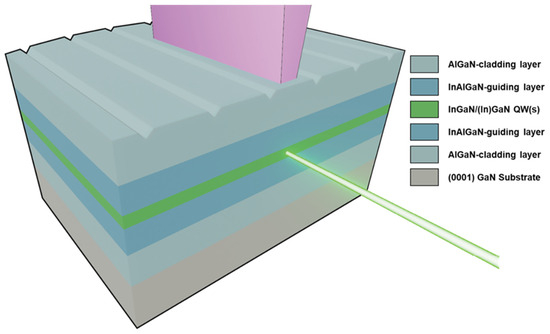
Figure 1.
Schematic of a green laser structure and an example of stimulated emission by optical pumping. (The purple area at the top represents the optical cavity, and the light emitted from the side of the sample represents the lasing light.)
While ultrafast spectroscopy provides high-resolution temporal dynamics of carrier behavior, the Variable Stripe Length Method (VSLM) was employed in this study due to its practical advantages in directly correlating optical gain with the physical cavity length of laser diode structures. VSLM allows for a straightforward assessment of steady-state gain saturation and spectral narrowing under conditions that closely mimic the operational environment of edge-emitting lasers [11]. However, it should be noted that VSLM can be sensitive to inhomogeneous carrier distribution along the stripe and gain guiding effects, which were carefully monitored during our measurements to ensure data consistency.
Prior to fabricating the laser diode structure, the optical gain behavior of the sample was evaluated using the Variable Stripe Length Method (VSLM) under a range of excitation densities [12]. A schematic of the VSLM optical setup is presented in Figure 2. To generate sufficiently high carrier densities, we employed the EKSPLA NT342 Series—a tunable nanosecond laser system combining a Q-switched Nd:YAG source with a nanosecond optical parametric oscillator. An excitation wavelength of 410 nm was selected to ensure preferential excitation of the active region. The incident laser beam was shaped into a 2-mm-long stripe, and a central 700 segment of this stripe was used as the effective excitation length to maintain uniform carrier distribution. Stripe lengths () of 150, 300, 350, 600, and 700 were examined, and excitation fluences of 0.95, 2.38, 4.75, 9.5, 23.8, and 33.25 were applied.
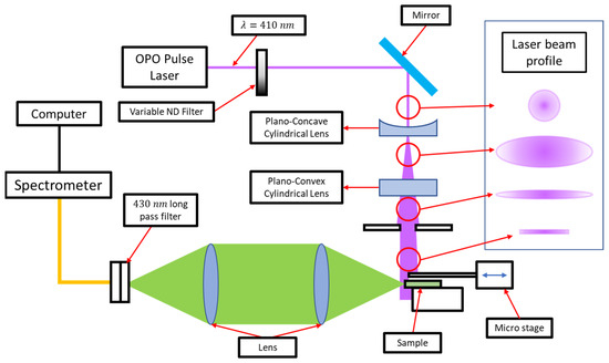
Figure 2.
Schematic representation of the VSLM optical measurement setup.
3. Results and Discussion
The evolution of the emission spectrum with varying stripe length at identical excitation densities is summarized in Figure 3. A comparison of spectra in Figure 3a,b reveals that increasing leads to spectral narrowing. For example, at a given excitation density, the full width at half maximum (FWHM) decreases from 23.4 nm for to 17.2 nm for . This trend—narrower FWHM at longer cavity lengths—was consistently observed across all measured stripe lengths, as illustrated in Figure 3c. Additionally, the excitation density corresponding to the onset of FWHM narrowing shifts to lower values as the stripe length increases, indicating that the threshold for stimulated emission decreases with increasing cavity length. As expected, the ASE threshold decreases as the stripe length increases. This behavior is consistent with established theoretical models for semiconductor gain media [13], where a longer gain path allows for a higher cumulative amplification, thereby lowering the required excitation density to reach the threshold.
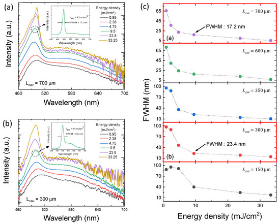
Figure 3.
Spectrum graphs with stripe length at (a) and (b) . (c) FWHM vs. excitation density for each stripe length. Red boxes show half-width graphs plotting the changes in excitation density in graphs (a) and (b).
A notable observation emerges when examining the shift in the peak emission wavelength. As shown in Figure 4, for stripe lengths from 150 up to 700 , the dominant emission at low excitation densities is spontaneous emission, accompanied by a blue shift in the peak wavelength. This behavior is consistent with band-filling effects at low carrier densities. As the excitation density increases further, spontaneous emission transitions into stimulated emission. Unlike spontaneous emission, the peak wavelength in the stimulated regime remains nearly stationary or shifts slightly to longer wavelengths. Because stimulated emission arises from cavity-induced optical feedback, its spectral position becomes decoupled from density-of-states variations within the semiconductor. The observed redshift of the emission peak at high excitation densities and extended stripe lengths is primarily attributed to localized Joule heating, which induces thermal bandgap shrinkage. Beyond thermal effects, the saturation of optical gain and the subsequent spectral shift are also influenced by the band-filling effect and the clamping of the quasi-Fermi level separation under high-density stimulated emission [14]. As the stimulated emission rate increases, the carrier density remains relatively constant due to gain clamping, while the increased lattice temperature further narrows the effective bandgap, leading to the observed spectral behavior.
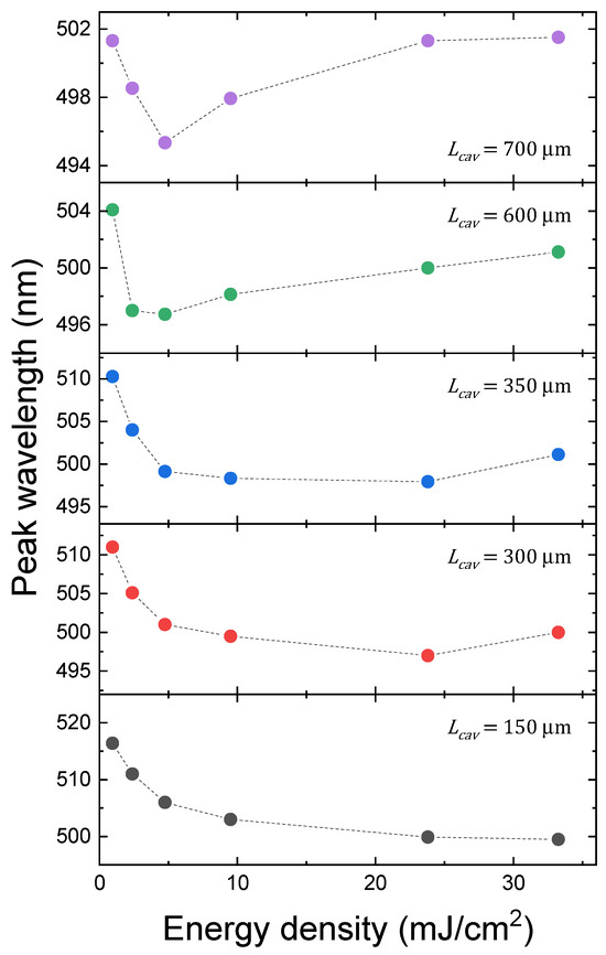
Figure 4.
Variations in the peak emission wavelength as a function of excitation density for different stripe lengths. The observed behavior reflects the interplay between the carrier-induced effects and thermal-induced redshifts at higher excitation levels for each .
The gain spectra were tested using Equation (1) [15].
where is the stripe length, and and denote the intensity vs. wavelength at 2 and , respectively. While more recent models for extracting optical gain have been proposed to account for specific experimental artifacts [16], Equation (1) remains a robust and foundational approach for the stripe length regime investigated in this study. In our experimental conditions, this model provided high fitting stability and consistent gain coefficients across varying excitation densities, allowing for a reliable comparative analysis of gain saturation effects. The gain spectra according to the stripe length were assessed by substituting into the equation. A comparison of graphs (a) and (b) in Figure 5 reveals that the gain increases as the excitation region increases even at the same density. This may be attributable to an increase in the amount of medium required for excitation as the stripe length increases, leading to the behavior associated with increased gain, while the gain per unit area remains similar. In addition, graphs in (b) show a partial decrease in gain at 23.8 as gain saturation is reached, with the main emission being stimulated emission. This suggests that the excitation density energy required for stimulated emission may vary depending on the aforementioned stripe length.
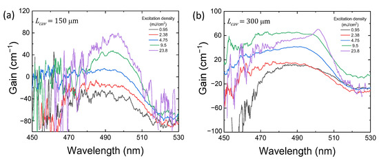
Figure 5.
Gain vs. excitation density at (a) and (b) .
.
The graphs in Figure 6 show changes in the maximum gain in the gain spectra. The graphs in (a) show that the maximum gain increases linearly with an increase in the excitation density at . At and , however, while the maximum gain is high at low excitation densities, the slope for the increase in the maximum gain decreases gradually as the excitation density increases, and the maximum gain seems to decrease. This phenomenon may be attributable to the aforementioned behavior associated with an increased maximum gain by the overall gain due to the increase in the excitation region at low excitation densities. As the excitation density increases, however, some of the carriers cannot contribute to radiative recombination because of Joule heating leading to an increase in the temperature ratio, with the slope for the increase in the maximum gain gradually decreasing. The graphs in (b) show that the maximum gain stops increasing from an excitation density of 23.8 onward, irrespective of the increase in the stripe length. This confirms the existence of an intersection at that indicates the critical point between the cavity length and excitation density required for stimulated emission.
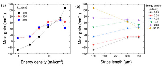
Figure 6.
Maximum gain vs. excitation density at (a) each stripe length and (b) each excitation.
Figure 7 shows the effect of gain saturation induced by an increase in the stripe length on the emission spectral properties. The graphs in (a) and (b) indicate that a blue shift occurs when the stripe length increases at a low excitation density of 0.95 ; gain saturation does not occur because the spontaneous emission is the main emission at all stripe lengths with a minimum half width of ~65 nm. In contrast, as the excitation density gradually increases, the peak wavelength hardly moves from 350 um onwards at an excitation density of 9.5 . As shown in Figure 7b, the full width at half maximum (FWHM) of the emission spectra exhibits a rapid decrease with increasing stripe length up to the threshold, signifying the onset of amplified spontaneous emission (ASE). Beyond the saturation point, however, the FWHM stabilizes or slightly broadens, which correlates with the gain saturation behavior discussed previously.
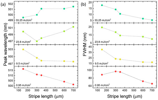
Figure 7.
(a) Peak wavelength vs. stripe length at each excitation density; (b) FWHM vs. stripe length at each excitation density.
After this point, the redshift properties become increasingly pronounced as a higher excitation density is applied to the stripe, which may be a consequence of gain saturation due to the stimulated emission, which acts as the main emission, coupled with the increasing Joule heating effect in the gradually increasing excitation region, leading to the manifestation of red shift properties of the wavelength.
4. Conclusions
Although extending the stripe length generally lowers the excitation density required to induce optical oscillation, our results indicate that a longer excitation region also accelerates gain saturation at comparable excitation densities. This effect is attributed to increased Joule heating, which leads to a red shift in the stimulated emission peak. As a result, maintaining laser operation at the desired wavelength becomes challenging when high-energy excitation is applied to achieve higher output power. These findings suggest that the cavity length must be optimized with careful consideration of the gain saturation behavior induced by thermal effects. Consequently, this work provides foundational insight into determining the optimal cavity dimensions—both length and width—when designing and fabricating high-performance laser diodes.
Author Contributions
Conceptualization, Y.S.K.; methodology, Y.S.J.; validation, Y.S.K., S.R.L. and S.-N.L.; resources, Y.S.K.; data curation, Y.S.J., S.R.L. and S.-N.L.; writing—original draft preparation, Y.S.J. and Y.S.K.; writing—review and editing, S.-N.L. and Y.S.K.; visualization, Y.S.J.; supervision, Y.S.K.; project administration, Y.S.K.; funding acquisition, Y.S.K. All authors have read and agreed to the published version of the manuscript.
Funding
This work was supported by the IITP (Institute of Information & Communications Technology Planning & Evaluation)-ICAN (ICT Challenge and Advanced Network of HRD) (IITP-2026-RS-2022-00156326, 50%) grant funded by the Korea government (the Ministry of Science and ICT) and by the 2025 sabbatical year research grant of the Tech University of Korea.
Institutional Review Board Statement
Not applicable.
Informed Consent Statement
Not applicable.
Data Availability Statement
Data are contained within the article.
Conflicts of Interest
The authors declare no conflicts of interest.
References
- Nakamura, S.; Senoh, M.; Iwasa, N.; Nagahama, S.; Yamada, T.; Mukai, T. Superbright Green InGaN Single-Quantum-Well-Structure Light-Emitting Diodes. Jpn. J. Appl. Phys. 1995, 34, L1332. [Google Scholar] [CrossRef]
- El-Masry, N.A.; Piner, E.L.; Liu, S.X.; Bedair, S.M. Phase separation in InGaN grown by metalorganic chemical vapor deposition. Appl. Phys. Lett. 1998, 72, 40–42. [Google Scholar] [CrossRef]
- Kojima, K.; Funato, M.; Kawakami, Y.; Nagahama, S.; Mukai, T.; Braun, H.; Schwarz, U.T. Gain Suppression Phenomena Observed in InxGa1-xN Quantum Well Laser Diodes Emitting at 470 nm. Appl. Phys. Lett. 2006, 89, 241127. [Google Scholar] [CrossRef]
- Miller, D.A.B.; Chemla, D.S.; Damen, T.C.; Gossard, A.C.; Wiegmann, W.; Wood, T.H.; Burrus, C.A. Band-Edge Electroabsorption in Quantum Well Structures: The Quantum-Confined Stark Effect. Phys. Rev. Lett. 1984, 53, 2173–2176. [Google Scholar] [CrossRef]
- Miyoshi, T.; Masui, S.; Okada, T.; Yamamoto, T.; Kozaki, T.; Nagahama, S.; Mukai, T. 510-515 nm InGaN-Based Green Laser Diodes on c-Plane GaN Substrate. Appl. Phys. Express 2009, 2, 062201. [Google Scholar] [CrossRef]
- Avramescu, A.; Lermer, T.; Müller, J.; Tautz, S.; Queren, D.; Lutgen, S.; Strauß, U. InGaN laser diodes with 50 mW output power emitting at 515 nm. Appl. Phys. Lett. 2009, 95, 071103. [Google Scholar] [CrossRef]
- Enya, Y.; Yoshizumi, Y.; Kyono, T.; Akita, K.; Ueno, M.; Adachi, M.; Sumitomo, T.; Tokuyama, S.; Ikegami, T.; Katayama, K.; et al. 531 nm Green Lasing of InGaN Based Laser Diodes on Semi-polar {20-11} Free-Standing GaN Substrates. Appl. Phys. Express 2009, 2, 082101. [Google Scholar] [CrossRef]
- Tao, R.; Arakawa, Y. Impact of quantum dots on III-nitride lasers: A theoretical calculation of threshold current densities. Jpn. J. Appl. Phys. 2019, 58, SCCC31. [Google Scholar] [CrossRef]
- Sugahara, T.; Sato, H.; Hao, M.; Naoi, Y.; Kurai, S.; Tottori, S.; Yamashita, K.; Nishino, K.; Romano, L.T.; Sakai, S. Direct Evidence That Dislocations Are Non-Radiative Recombination Centers in GaN. Jpn. J. Appl. Phys. 1998, 37, 398–400. [Google Scholar] [CrossRef]
- Grandjean, N.; Damilano, B.; Dalmasso, S.; Leroux, M.; Laugt, M.; Massies, J. Built-in electric-field effects in wurtzite GaN/AlGaN quantum wells. J. Appl. Phys. 1999, 86, 3714. [Google Scholar] [CrossRef]
- Dal Negro, L.; Cazzanelli, M.; Pavesi, L.; Ossicini, S.; Pacifici, D.; Franzo, G.; Priolo, F.; Iacona, F. Dynamics of stimulated emission in silicon nanocrystals. Appl. Phys. Lett. 2003, 82, 4636–4638. [Google Scholar] [CrossRef]
- Shaklee, K.L.; Nahory, R.E.; Leheny, R.F. Optical Gain in Semiconductors. J. Lumin. 1973, 7, 284–309. [Google Scholar] [CrossRef]
- Cerdan, L.; Costela, A.; Garcia-Moreno, I. On the characteristic lengths in the variable stripe length method for optical gain measurements. J. Opt. Soc. Am. 2010, 27, 1874–1877. [Google Scholar] [CrossRef]
- Chuang, S.L. Physics of Photonic Devices, 2nd ed.; Chapter on Gain Clamping and Semiconductor Laser Physics; Wiley: Hoboken, NJ, USA, 2009. [Google Scholar]
- Hvam, J.M. Direct Recording of Optical-gain Spectra from ZnO. J. Appl. Phys. 1978, 49, 3124–3126. [Google Scholar] [CrossRef]
- Milanese, S.; De Giorgi, M.L.; Anni, M.; Bondnarchuk, M.I.; Cerdan, L. Rationalizing the Amplified Spontaneous Emission Mechanism in CsPbBr3 Perovskite Nanocrystals Films by means of Optical Gain Measurements. Adv. Opt. Mater. 2024, 12, 2401078. [Google Scholar] [CrossRef]


Disclaimer/Publisher’s Note: The statements, opinions and data contained in all publications are solely those of the individual author(s) and contributor(s) and not of MDPI and/or the editor(s). MDPI and/or the editor(s) disclaim responsibility for any injury to people or property resulting from any ideas, methods, instructions or products referred to in the content. |
© 2026 by the authors. Licensee MDPI, Basel, Switzerland. This article is an open access article distributed under the terms and conditions of the Creative Commons Attribution (CC BY) license.