Abstract
Thin-film lithium niobate (TFLN) electro-optic modulators (EOMs) offer distinct advantages, including high speed, broad bandwidth, and low power consumption. However, their large size hinders the density of integration, which trades off with the half-wave voltage. Photonic crystal (PC) structures can effectively reduce the device footprint via the slow-light effect; however, they experience significant losses due to fabrication defects and sharp corners. Here, we theoretically demonstrate an ultracompact Mach–Zehnder interferometer (MZI) EOM based on a TFLN valley photonic crystal (VPC) structure. The design can achieve a high forward transmittance (>0.8) due to defect-immune unidirectional propagation in the VPC, enabled by the unique spin-valley locking effect. The EOM, with a small footprint of 21 μm × 17 μm, achieves an extinction ratio of 16.13 dB and a modulation depth of 80%. The design can be experimentally fabricated using current nanofabrication techniques, making it suitable for broad applications in optical communications.
1. Introduction
Electro-optic modulators (EOMs) are crucial devices in optical communication [1,2,3,4] and quantum computing systems [5,6,7], which utilize electrical signals to modulate light, serving as an interface between electronics and photonics. Due to its strong electro-optic effect, lithium niobate (LN) is considered the most promising material for EOM applications, offering a broad operating wavelength range and a large working bandwidth [8]. The electro-optical coefficient of LN is much higher than that of other semiconductor materials, such as silicon [9,10,11], silicon nitride [12,13], and indium phosphide [14], enabling the design of high-performance, highly efficient EOMs that meet the needs of high-speed optical communication systems.
Currently, significant progress has been made in modulator technology, and the recent development of thin-film lithium niobate (TFLN) enables a higher refractive-index contrast, achieving low-loss rigid waveguides and a lower half-wave voltage (HWV, the voltage required to achieve a π phase shift) [15,16,17]. Various TFLN EOMs based on different device architectures have been demonstrated, including the Michelson interferometer (MI) [18,19], ring resonators [20], and the Mach–Zehnder interferometer (MZI) [15]. The basic principle of the MI modulator is to divide the incident light into two coherent beams via amplitude-splitting interference, so that at least one of the beams traverses the modulation path twice, thereby doubling the optical path difference, and finally achieving light intensity modulation through interference. Its advantage is that ‘double-pass modulation’ can halve the device length, thereby improving modulation efficiency [21]. However, this approach suffers from high intrinsic loss due to superimposed waveguide propagation loss, interface reflection loss, and other factors, resulting in low output optical power. TFLN ring resonator modulators apply an electric field to the ring resonator, which alters the refractive index, changing the phase of light [22], which can achieve a high modulation efficiency and low power consumption. More importantly, it is necessary to use a low Q-factor to improve bandwidth, but at the expense of modulation efficiency, thus failing to meet the requirements of high bandwidth and high efficiency simultaneously.
In comparison, the MZI EOMs exhibit substantial advantages in optical communications, distinguished by their high-speed modulation capability, enabling the transmission of signals with bandwidths ranging from tens to hundreds of GHz and ensuring stable, high-rate transmission. However, conventional MZI EOMs are based on the normal dispersion of the waveguide modes, because of which the required HWV is inversely proportional to the length of the waveguide. As a result, it generally requires a large size to achieve a low HWV [17,23,24]. Consequently, efforts have been made to develop novel structures, such as photonic crystals (PCs) [25,26,27], metasurfaces [28], and plasmonic devices [29]. The slow-light effect in PC structures can significantly increase the effective refractive index of PC waveguides, thereby reducing the required length to achieve miniaturized designs. However, the transmittance of PC waveguides is highly sensitive to fabrication-related structural defects, compromising their performance [30,31,32,33].
Recent developments in topological photonic crystals (TPCs) enable the achievement of defect-immune unidirectional transmission. Among different types of TPC structures, valley photonic crystals (VPCs) offer a simple design process and a large working bandwidth [34,35]. More importantly, VPCs can use dielectric materials without requiring an external magnetic field. As a result, silicon VPC structures have been demonstrated [36,37]. Our previous work has shown that the slow-light effects of topological edge states can effectively enhance the electro-optic effect in lithium niobate VPC waveguides, achieving a low HWV with an ultracompact footprint. However, MZI EOMs based on lithium niobate VPC structures have not been demonstrated.
Here, we theoretically demonstrate an ultracompact MZI electro-optic amplitude modulator based on a thin-film lithium niobate (TFLN) VPC structure. The design can achieve a high forward transmittance (>0.8) due to defect-immune unidirectional propagation in the VPC, enabled by the unique spin-valley locking effect. The EOM with a small footprint of 21 μm × 17 μm achieves an extinction ratio of 16.13 dB and a modulation depth of 80%. The design can be experimentally fabricated using current complementary metal-oxide-semiconductor (CMOS) nanofabrication techniques, making it suitable for a wide range of optical communication applications.
2. Design of Thin-Film Lithium Niobate MZI EOM Based on VPC Structures
The conceptual demonstration of the MZI EOM based on the VPC structure is shown in Figure 1a. The MZI structure is constructed by two Ω-shaped topological waveguides formed by combining two mirror-inverted VPC structures, which compose triangular airholes in the free-standing TFLN substrate. The gold electrodes are deposited on both sides of one waveguide (3 μm apart) to apply an electric field. Compared with Al and TiN, gold exhibits higher electrical conductivity and superior chemical stability. Additionally, the fabrication process for gold electrodes is well-established and has been widely adopted in lithium niobate modulator research. The strong electro-optic (EO) effect of LN can introduce refractive modulation in response to an external voltage, thereby producing a phase difference between the two waveguides. The simulated electric field distribution (using COMSOL Multiphysics 6.2 software) is shown in Figure 1b. The thin-film design enables the strongest electric field to cross the waveguide, thereby minimizing the required voltage. The proposed device employs a single-arm modulation scheme. The working scenarios are schematically shown in Figure 1c,d, in which the incident beam is split at the first Y-junction and combined to interfere at the second Y-junction. The line and arrows indicate the optical paths. The interference results are decided by the phase difference φd between the two waveguides (arms). The EOM is designed to achieve destructive interference (φd = nπ, n is an odd number) when the external voltage is 0 V (Figure 1c), and constructive interference is achieved when a HWV is applied, resulting in a phase difference of φd = 2 nπ, where n is an integer. This design employs a 220 nm-thick x-cut LN thin film to exploit the largest EO coefficient (r33) [25]. Due to the Pockels effect, LN exhibits an EO response with a direct current (DC) electric field [38], which can be formulated as follows:
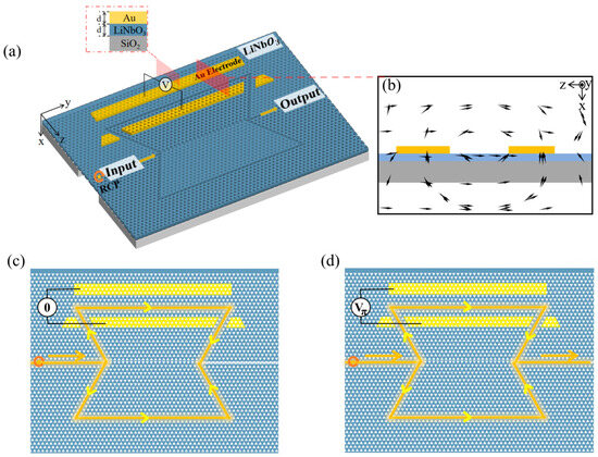
Figure 1.
Conceptual design of MZI EOM based on lithium niobate VPC structure. (a) 3D schematic of MZI EOM based on a lithium niobate VPC structure and cross-sectional view of the device. The thickness of the TFLN and the gold electrode are both d = 220 nm (the star represents right-handed circularly polarized light). (b) Simulated electric field distribution inside the EOM by applying an external voltage, where the arrow indicates the vectorial direction of the electric field. (c) Schematic of destructive interference when the external voltage is 0 V. (d) Schematic of constructive interference when the external voltage is HWV. The arrows indicate the direction of light propagation.
Among these, nx, ny, and nz are the refractive indices of LN with an external voltage in the x, y, and z directions; no and ne are the ordinary and extraordinary refractive indices, respectively; r13 and r33 are the two Pockels coefficients of LN. In our design, since an x-cut LN thin film is used (Figure 1a), the EO coefficient r33 is employed for modulation. To quantify the Pockels effect, we calculate the local-field factor within the device using a previously published method [39,40]. For the LN PC structure, we define the effective EO effect as expressed in Equation (2):
where fi (i = 1, 2, 3) are the local field factors of the three waves involved in the second-order process. denotes the group velocity of bulk LN material without nanostructures, which is . Meanwhile, is the group velocity of the modes within the PC structure, which is . From Equations (2) and (3), it can be seen that maximizing the EO coefficient is an effective means to achieve maximal effective refractive index modulation. This means that the group velocity of the PC structure must be minimized, since is a constant only depending on the material.
In order to design the VPC structures, we first create a honey PC structure with C6v symmetry (the unicell comprises two sets of triangular air holes, rA = rB = 90 nm, which is defined as the distance between the vertex and geometric center of the triangle), which shows a Dirac cone structure in the photonic band diagram of transverse electric (TE) polarized mode. The lattice constant of the structure is a = 440 nm. By changing the size of the triangular holes (rA = 180 nm, rB = 0 nm), valley photonic crystals VPC1 and VPC2 are obtained, which are reduced to C3 symmetry. The K and K’ points degenerate and form a photonic bandgap. Since VPC1 and VPC2 are mirror symmetric, the photonic band diagrams of VPC1 and VPC2 are the same (the details of the design process are shown in Supplementary Materials Section S1) [41,42,43]. By combining VPC1 and VPC2, two configurations form waveguides that support topological edge states, namely, zigzag- and beard-type boundaries. Figure 2a,b shows the dispersion relations of beard-type and zigzag-type boundaries. Compared to the beard-type boundary, the zigzag-type boundary features high transmittance, low loss, and broad working bandwidth (the details of the design process are shown in Supplementary Materials Section S2). Therefore, the zigzag-type waveguide is selected for constructing the electrically tunable MZI in this study. In this work, commercial software (Lumerical FDTD2020) based on the finite-difference time-domain (FDTD) method is used for simulation.
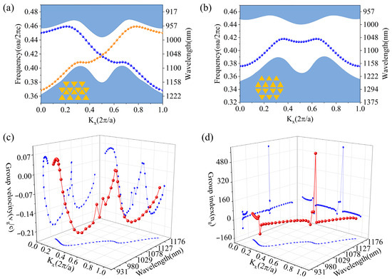
Figure 2.
(a) Edge state plots (dotted lines) of the zigzag (a) and beard (b) type boundary structures (The shaded blue regions represent the bulk bands. The blue and orange dotted lines in (a) represent the two pseudospin states). Plots (red dotted lines) of normalized group velocity (vg/c) (c) and group refractive index (ng) (d) versus Kx (blue dotted lines) and wavelength (blue dotted lines) of the zigzag-type boundary.
The vg and ng of the edge states can be calculated as and [44]. Therefore, vg represents the slope of the edge state and can be zero at the maximum and minimum points on the edge state plot. The vg and ng plots of the zigzag-type boundary are shown in Figure 2c,d. The calculations indicate that the edge states of the zigzag-type boundary can achieve a vg of zero at the point , which corresponds to the minimum of the standing wave mode. However, in real applications, this point cannot be utilized since the mode cannot propagate through waveguides. Therefore, we select a point near vg = 0 at 1077 nm to achieve a relatively low vg and high ng. At this point, the group velocity vg/c is 0.00180036, and the group refractive index ng is 555. According to r33 of the x-cut TFLN (32 pm/V [45], the is calculated as 131,072 pm/V.
To construct an MZI, we first design an Ω-shaped waveguide with a zigzag-type boundary because the light path along each arm of the MZI is along an Ω-shaped trajectory, as shown in Figure 3a, where the orange blocks indicate the electrodes. The forward transmittance spectrum and the electric field intensity distribution under 0 V are shown in Figure 3c (black curve) and Figure 3e. The zigzag-type boundary features high transmittance (0.92), low loss, and a relatively broad bandwidth of 68 nm. (details are provided in Supplementary Materials Section S3). It should be noted that group velocity dispersion (GVD), inherent to slow-light systems, narrows the effective operating bandwidth in high-speed applications. This further demonstrates the VPC’s excellent anti-scattering performance, enabling light to pass through sharp corners without strong reflection or scattering. Due to the EO effect, the refractive index of LN changes with the applied voltage, and the corresponding refractive index modulation formula is as follows [39]:
where s is the gap between electrodes, and there is a linear relationship between the applied voltage and the change in refractive index. As shown in Figure 3d, when a voltage (Vπ) is applied in the orange region, a π-phase modulation is generated. We set the voltage change to 0.0538 V (corresponding to the refractive index change of 0.0125) (the details of the design process are shown in Supplementary Materials Section S4). The edge-state curves at different voltages are shown in Figure 3b, and it can be seen that the working wavelength red-shifts as the voltage on the Ω-shaped waveguide is sequentially increased, because the effective refractive index increases with increasing applied voltage. Meanwhile, the forward transmittance spectrum and the electric field intensity distributions at Vπ remain similar to those at 0 V, as shown in Figure 3c,f confirm that phase-only modulation can be achieved. In addition, the phase distributions confirm the achievement of π phase modulation as shown in Figure 3d.
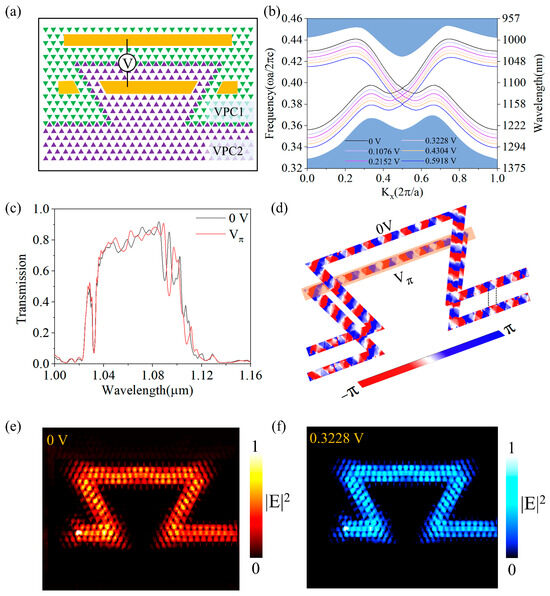
Figure 3.
(a) The Ω-shaped waveguide based on zigzag-type boundary with gold electrodes (The green and purple triangles represent the unit cells of the valley photonic crystals VPC1 and VPC2, respectively). (b) Edge state curves under different voltages. (c) The transmittance curve under 0 V and Vπ. (d) Phase modulation at 0 V and Vπ. (e,f) Electric field intensity distributions at 0 V and Vπ, respectively.
3. Performance Analysis of the MZI EOM
We can see from Figure 4a that the MZI structure consists of two topological straight waveguides and two Ω-shaped interference arms, L1 and L2, represented by black and red lines, respectively. The MZI’s principle is based on the interference effect of two optical waveguides. In the MZI, the incident light first passes through a straight waveguide of length 13a and is split into two identical beams, which then pass through the interference arms L1 (L1 = 66a) and L2 (L2 = 63a). The difference in the length of the two arms is 5a (ΔL = 5a). When light is transmitted, a phase difference is established between the two interference arms. Consequently, following the combination of these two light beams and the subsequent occurrence of interference, the presence of this phase difference gives rise to a change in the intensity of the light power at the final output end. The phase difference between the two interference arms can be expressed as follows:
where n1 and n2 are the effective refractive indices of the interference arms L1 and L2, n1 = n2 (V = 0 V). l1 and l2 are the lengths of the interference arms L1 and L2, respectively. A π phase difference is usually required between the arms to achieve destructive interference and to obtain a near-zero valley at the designed wavelength.
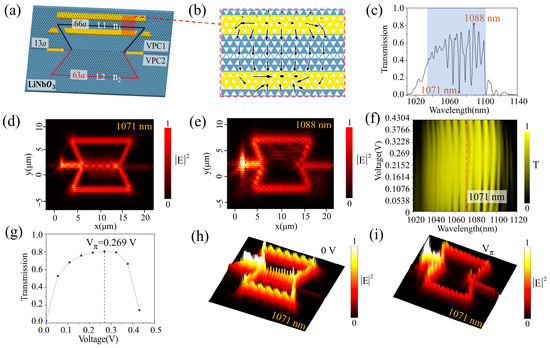
Figure 4.
(a) 3D schematic of the designed VPC MZI structure. The red and blue colors represent different arms of the MZI structure. (b) Simulated electric field distribution inside the EOM by applying an external voltage, where the arrows indicate the vectorial direction of the electric field. (c) Transmission spectrum of MZI. Electric field intensity distributions of incident light at the wavelengths of 1071 nm (d) and 1088 nm (e). (f) The transmission surface plot of an MZI EOM at different external voltages and wavelengths. (g) Transmission plot at 1071 nm at different external voltages. Electric field intensity distribution at 1071 nm at the voltage of 0 V (h) and Vπ (0.269 V) (i).
The light intensity at the output can be expressed as follows:
where A1 and A2 denote the amplitude of the light waves in the two interference arms, respectively, and φd is the phase difference shown in Equation (6). The forward transmittance spectrum of the VPC MZI structure (V = 0 V) is shown in Figure 4c. Due to the high forward transmittance within the wavelength range of 1043–1099 nm, one can see distinct interference peaks (close to 1) and valleys (near zero) in the spectrum. The electric field distributions of MZI (V = 0 V) at different wavelengths are plotted in Figure 4d,e, which correspond to the constructive interference at 1088 nm and destructive interference at 1071 nm.
The extinction ratio, insertion loss, modulation depth, and sensitivity of MZIs are key performance indicators. When constructive interference (φd = an integer multiple of 2π) is achieved, the output power is Pon, and when destructive interference (φd =π) occurs, the output power is Poff. The extinction ratio of the MZI can be expressed as Equation (8):
The insertion loss of the MZI can be expressed as Equation (9):
Assuming that the maximum output power of MZI is Pmax and the minimum output power is Pmin during the modulation process, the modulation depth of MZI can be expressed as Equation (9):
Subsequently, a voltage is applied to the arm L1. Due to the strong EO effect of LN, the effective refractive index n1 of L1 changes (n1 ≠ n2), which affects the phase of L1. Thus, the position of the peaks (constructive interference) and valleys (destructive interference) in the transmission spectrum can be well controlled by applying a voltage to one arm. This approach successfully modulates light intensity at a selected wavelength. The simulated electric field distribution (COMSOL Multiphysics) is shown in Figure 4b, revealing a strong electric field across the waveguide, providing the strongest electro-optical modulation. The applied voltage of the TFLN substrate ranges from 0 V to 0.4304 V with a gradient of 0.0538 V corresponding to the index change of 0.0125 of L1. The forward transmission spectra at different voltages are shown in Figure 4f (details are provided in Supplementary Materials Section S5). Here, 1071 nm in the working bandwidth is selected as an example for specific analysis. As the applied voltage changes, the device’s transmission changes accordingly, as shown in Figure 4g.
The figure shows that at 0 V and an input light wavelength of 1071 nm, the device produces destructive interference, resulting in the lowest observed transmission of 0.02. At an applied voltage of 0.269 V, the device exhibits constructive interference, yielding a maximum transmission of 0.82. The distributions of electric field intensity are depicted in Figure 4h,i. The high transmittance in the constructive interference peak is attributed to the efficient light splitting and combining at the Y-junctions, and the back-reflection remains consistently low (<0.1) throughout the working bandwidth (details are provided in Supplementary Materials Section S6). Thus, we realize intensity modulation at the selected wavelength, as calculated using Equations (8)–(10); the device’s extinction ratio is 16.13 dB, the insertion loss is 0.86 dB, and the modulation depth is 80%. The Vπ is 0.269 V.
It is worth noting that as the refractive index of the LN waveguide increases with applied voltage, the bandgap redshifts. We conducted simulation analyses of edge states under different externally applied voltages, and the resulting dispersion curves are shown in Figure 5a. As shown in Figure 5b, the central wavelength of the bandgap redshifts along with the voltage increase. When the externally applied voltage is 0.6994 V, the bandgap exhibits a passband in the range of 0.368 a/λ–0.411 a/λ (1071 nm–1196 nm), which deviates slightly from the target wavelength of 1071 nm. Therefore, the maximum applied voltage should not exceed 0.6994 V. In principle, this method can be applied to design MZI EOM working at any wavelength by changing the geometry of the MZI. Furthermore, by adjusting the VPC parameters, the spectrum can be extended towards 1550 nm. (details are provided in Supplementary Materials Section S7).
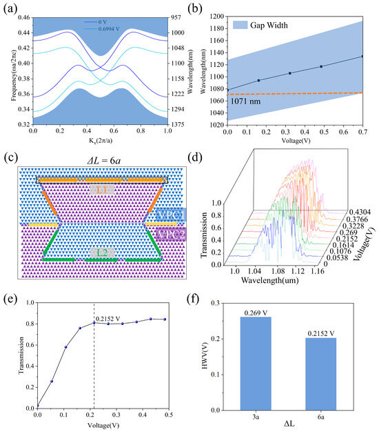
Figure 5.
(a) Edge state curves under externally applied voltages of 0 V and 0.6994 V; (b) The tuning curve of the photonic bandgap range with voltage. (c) Schematic diagrams of the structure when the arm length difference ΔL = 6a. The blue and purple colors represent VPC1 and VPC2, respectively. The yellow arrows represent the entry and exit waveguides of the MZI structure. The orange and green colors represent the optical waveguides of the arms L1 and L2, respectively. (d) The transmission plots of the MZI EOM (ΔL = 6a) with different voltages at different wavelengths. (e) Localized magnification of the transmittance at 1075 nm. (f) The comparison bar chart of the HWV of ΔL = 3a and ΔL = 6a.
Based on the optical intensity modulation, we further studied the influence of different arm length differences, ΔL, on the half-wave voltage. The relationship between arm length difference and half-wave voltage can be expressed as follows:
where s is the gap between electrodes and φd is the phase difference shown in Equation (6). It can be seen from Equation (11) that the HWV is inversely proportional to ΔL, and the larger the ΔL, the smaller the HWV. Here, we selected the length difference between the two arms of ΔL = 6a, whose geometry is shown in Figure 5c. The transmission spectra of the MZI EOM with different voltages at an arm-length difference of ΔL = 6a are shown in Figure 5d, which exhibit distinct changes with voltage (details are shown in Supplementary Materials Section S8). Due to the high forward transmittance in the wavelength range of 990–1140 nm, the MZI shows distinct interference peaks (close to 1) and valleys (close to 0). Due to the differences in interference spectra, we chose different wavelengths for this arm length. Through analysis and verification, we selected 1075 nm (for ΔL = 6a), as shown in Figure 5e. As shown in Figure 5f, with the increase in the arm length difference, the HWV decreases, which is as expected from Equation (11). Furthermore, we present a discussion on the manufacturing tolerances of the corner rounding in VPC design in the Supplementary Materials Section S9, allowing us to define the required fabrication accuracy.
4. Conclusions
In conclusion, we have designed a thin-film lithium niobate MZI EOM based on a VPC structure. The EO effect of LN was used to design the EOM, and the phase change at the output was achieved by applying a voltage, thereby changing the LN’s refractive index. The modulator not only achieves a compact size (21 μm × 17 μm) but also exhibits excellent optical performance, including a peak forward transmittance of 0.82, an extinction ratio of 16.13 dB, and a modulation depth of 80%. The thin-film lithium niobate VPC MZI electro-optical modulators are expected to contribute to next-generation optical networks with their high-speed modulation, low loss, and ease of integration, helping realize higher speeds and broader bandwidth for optical signals.
Supplementary Materials
The following supporting information can be downloaded at: https://www.mdpi.com/article/10.3390/photonics13010033/s1, Figure S1: A schematic of the photonic crystal and photonic band diagram. Figure S2: (a) Schematic diagram of the zigzag-type boundary. (b) Schematic diagram of the beard-type boundary. (c) The transmittance spectrum of the straight waveguide based on the zigzag-type boundary. (d) The transmittance spectrum of the straight waveguide based on the beard-type boundary. Figure S3: (a) Ω-shaped waveguide assembled by zigzag-type boundary, corresponding transmittance (c) and electric field distribution at 1071 nm (e); (b) Ω-shaped waveguide assembled by beard-type boundary, corresponding transmittance (d) and electric field distribution at 1064 nm (f). Figure S4: The refractive index of LN changes with the applied voltage. Figure S5: Transmittance diagram of MZI at different voltages. Figure S6: Transmission analysis of the Y-junction of the MZI structure. Figure S7: Photonic band diagrams of the original honeycomb PC and VPC structures. Figure S8: Transmittance plots of MZI with ΔL=6a at different voltages. Figure S9: A schematic of the honeycomb PC and photonic band diagram.
Author Contributions
Conceptualization, Y.Y., H.F., M.Z. and H.L.; methodology, Y.Y. and H.F.; software, Y.Y.; validation, H.F., X.L., M.Z. and H.L.; formal analysis, Y.Y. and H.F.; investigation, Y.Y. and H.F.; resources, H.F.; data curation, Y.Y.; writing—original draft preparation, Y.Y. and H.F.; writing—review and editing, Y.Y., H.F. and H.L.; visualization, X.L.; supervision, H.F.; project administration, H.F.; funding acquisition, H.F., P.D. and J.R. All authors have read and agreed to the published version of the manuscript.
Funding
This research was funded by the National Key Research and Development Program of China (Grant No. 2022YFA1404201), the Australia Research Council (Grant Nos. DP220100603 and FT220100559, LP210200345, and LP210100467), the National Natural Science Foundation of China (Grant No. U23A20375), the Natural Science Foundation of Shanxi Province (Grant No. 202403021211011), the Research Project Supported by Shanxi Scholarship Council of China (Grant No. 2024-032), The Fund Program for the Scientific Activities of Selected Returned Overseas Professionals in Shanxi Province (Grant No. 20240006), the Program of State Key Laboratory of Quantum Optics and Quantum Optics Devices (Grant No. KF202402), the Basic scientific research conditions and major scientific instrument and equipment development of Anhui Science and Technology Department (Grant No. 2023YFF0715700), and the Key Research project of Shanxi Province (Grant No. 2023021501010001).
Institutional Review Board Statement
Not applicable.
Informed Consent Statement
Not applicable.
Data Availability Statement
The data that support the findings of this study are available from the corresponding author upon reasonable request.
Acknowledgments
The authors acknowledge the useful discussions and suggestions from Yuan Tian.
Conflicts of Interest
Author Pengqi Dong was employed by the institute of architectural design and research of Taiyuan university of technology Co, Ltd. Author Junjun Ren was employed by Shanxi Chenghaoxin Intelligent Technology Co., Ltd. The remaining authors declare that the research was conducted in the absence of any commercial or financial relationships that could be construed as a potential conflict of interest.
References
- Zhang, Y.; Shen, J.; Li, J.; Wang, H.; Feng, C.; Zhang, L.; Sun, L.; Xu, J.; Liu, M.; Wang, Y.; et al. High-speed electro-optic modulation in topological interface states of a one-dimensional lattice. Light Sci. Appl. 2023, 12, 206. [Google Scholar] [CrossRef]
- Sinatkas, G.; Christopoulos, T.; Tsilipakos, O.; Kriezis, E.E. Electro-optic modulation in integrated photonics. J. Appl. Phys. 2021, 130, 010901. [Google Scholar] [CrossRef]
- Miller, D.A.B. Attojoule Optoelectronics for Low-Energy Information Processing and Communications. J. Light. Technol. 2017, 35, 346–396. [Google Scholar] [CrossRef]
- Koeber, S.; Palmer, R.; Lauermann, M.; Heni, W.; Elder, D.L.; Korn, D.; Woessner, M.; Alloatti, L.; Koenig, S.; Schindler, P.C.; et al. Femtojoule electro-optic modulation using a silicon–organic hybrid device. Light Sci. Appl. 2015, 4, e255. [Google Scholar] [CrossRef]
- Xu, W.; Guo, T.; Zhang, K.; Li, Z.; Zhou, T.; Zuo, Q.; Sheng, Y.; Jing, L.; Ma, H.; Yu, M.; et al. Manipulations of a transmon qubit with a null-biased electro-optic fiber link. Nat. Commun. 2025, 16, 2629. [Google Scholar] [CrossRef] [PubMed]
- Pittaluga, M.; Lo, Y.S.; Brzosko, A.; Woodward, R.I.; Scalcon, D.; Winnel, M.S.; Roger, T.; Dynes, J.F.; Owen, K.A.; Juárez, S.; et al. Long-distance coherent quantum communications in deployed telecom networks. Nature 2025, 640, 911–917. [Google Scholar] [CrossRef]
- Kues, M.; Reimer, C.; Roztocki, P.; Cortés, L.R.; Sciara, S.; Wetzel, B.; Zhang, Y.; Cino, A.; Chu, S.T.; Little, B.E.; et al. On-chip generation of high-dimensional entangled quantum states and their coherent control. Nature 2017, 546, 622–626. [Google Scholar] [CrossRef]
- Qi, Y.; Li, Y. Integrated lithium niobate photonics. Nanophotonics 2020, 9, 1287–1320. [Google Scholar] [CrossRef]
- Teng, M.; Fathpour, S.; Safian, R.; Zhuang, L.; Honardoost, A.; Alahmadi, Y.; Polkoo, S.S.; Kojima, K.; Wen, H.; Renshaw, C.K.; et al. Miniaturized Silicon Photonics Devices for Integrated Optical Signal Processors. J. Light. Technol. 2020, 38, 6–17. [Google Scholar] [CrossRef]
- Sun, C.; Wade, M.T.; Lee, Y.; Orcutt, J.S.; Alloatti, L.; Georgas, M.S.; Waterman, A.S.; Shainline, J.M.; Avizienis, R.R.; Lin, S.; et al. Single-chip microprocessor that communicates directly using light. Nature 2015, 528, 534–538. [Google Scholar] [CrossRef]
- Han, C.; Zheng, Z.; Shu, H.; Jin, M.; Qin, J.; Chen, R.; Tao, Y.; Shen, B.; Bai, B.; Yang, F.; et al. Slow-light silicon modulator with 110-GHz bandwidth. Sci. Adv. 2023, 9, eadi5339. [Google Scholar] [CrossRef]
- Skandalos, I.; Bucio, T.D.; Mastronardi, L.; Yu, G.; Zilkie, A.; Gardes, F.Y. A 100 Gb s−1 quantum-confined Stark effect modulator monolithically integrated with silicon nitride on Si. Commun. Eng. 2025, 4, 82. [Google Scholar] [CrossRef] [PubMed]
- Li, B.; Yuan, Z.; Williams, J.; Jin, W.; Beckert, A.; Xie, T.; Guo, J.; Feshali, A.; Paniccia, M.; Faraon, A.; et al. Down-converted photon pairs in a high-Q silicon nitride microresonator. Nature 2025, 639, 922–927. [Google Scholar] [CrossRef]
- Ogiso, Y.; Ozaki, J.; Ueda, Y.; Kashio, N.; Kikuchi, N.; Yamada, E.; Tanobe, H.; Kanazawa, S.; Yamazaki, H.; Ohiso, Y.; et al. Over 67 GHz Bandwidth and 1.5 V Vπ InP-Based Optical IQ Modulator With n-i-p-n Heterostructure. J. Light. Technol. 2017, 35, 1450–1455. [Google Scholar] [CrossRef]
- Wang, C.; Zhang, M.; Chen, X.; Bertrand, M.; Shams-Ansari, A.; Chandrasekhar, S.; Winzer, P.; Lončar, M. Integrated lithium niobate electro-optic modulators operating at CMOS-compatible voltages. Nature 2018, 562, 101–104. [Google Scholar] [CrossRef]
- Valdez, F.; Mere, V.; Wang, X.; Boynton, N.; Friedmann, T.A.; Arterburn, S.; Dallo, C.; Pomerene, A.T.; Starbuck, A.L.; Trotter, D.C.; et al. 110 GHz, 110 mW hybrid silicon-lithium niobate Mach-Zehnder modulator. Sci. Rep. 2022, 12, 18611. [Google Scholar] [CrossRef]
- Stokowski, H.S.; McKenna, T.P.; Park, T.; Hwang, A.Y.; Dean, D.J.; Celik, O.T.; Ansari, V.; Fejer, M.M.; Safavi-Naeini, A.H. Integrated quantum optical phase sensor in thin film lithium niobate. Nat. Commun. 2023, 14, 3355. [Google Scholar] [CrossRef]
- Huang, X.; Liu, Y.; Li, Z.; Guan, H.; Wei, Q.; Tan, M.; Li, Z. 40 GHz high-efficiency Michelson interferometer modulator on a silicon-rich nitride and thin-film lithium niobate hybrid platform. Opt. Lett. 2021, 46, 2811–2814. [Google Scholar] [CrossRef] [PubMed]
- Ghoname, A.O.; Hassanien, A.E.; Goddard, L.L.; Gong, S. Compact Lithium Niobate Michelson Interferometer Modulators Based on Spiral Waveguides. IEEE J. Sel. Top. Quantum Electron. 2024, 30, 3400108. [Google Scholar] [CrossRef]
- Wang, P.-Y.; Wan, S.; Zhang, M.; Ma, R.; Bo, F.; Shen, Z.; Wan, W.; Sun, F.-W.; Guo, G.-C.; Dong, C.-H. Dynamic Control of Non-Hermitian On-Site Potential in the Lithium Niobate Microresonator. Laser Photon. Rev. 2025, 19, e00552. [Google Scholar] [CrossRef]
- Jian, J.; Xu, M.; Liu, L.; Luo, Y.; Zhang, J.; Liu, L.; Zhou, L.; Chen, H.; Yu, S.; Cai, X. High modulation efficiency lithium niobate Michelson interferometer modulator. Opt. Express 2019, 27, 18731–18739. [Google Scholar] [CrossRef]
- Wang, C.; Zhang, M.; Stern, B.; Lipson, M.; Lončar, M. Nanophotonic lithium niobate electro-optic modulators. Opt. Express 2018, 26, 1547–1555. [Google Scholar] [CrossRef]
- Wei, C.; Feng, H.; Ye, K.; Eijkel, M.; Klaver, Y.; Chen, Z.; Keloth, A.; Wang, C.; Marpaung, D. Programmable multifunctional integrated microwave photonic circuit on thin-film lithium niobate. Nat. Commun. 2025, 16, 2281. [Google Scholar] [CrossRef]
- Tao, Z.; Wang, H.; Feng, H.; Guo, Y.; Shen, B.; Sun, D.; Tao, Y.; Han, C.; He, Y.; Bowers, J.E.; et al. Ultrabroadband on-chip photonics for full-spectrum wireless communications. Nature 2025, 645, 80–87. [Google Scholar] [CrossRef]
- Li, M.; Ling, J.; He, Y.; Javid, U.A.; Xue, S.; Lin, Q. Lithium niobate photonic-crystal electro-optic modulator. Nat. Commun. 2020, 11, 4123. [Google Scholar] [CrossRef]
- Fei, H.; Wu, M.; Lin, H.; Liu, X.; Yang, Y.; Zhang, M.; Cao, B. An on-chip nanophotonic reciprocal optical diode for asymmetric transmission of the circularly polarized light. Superlattices Microstruct. 2019, 132, 106155. [Google Scholar] [CrossRef]
- Du, Z.; Liao, K.; Dai, T.; Wang, Y.; Gao, J.; Huang, H.; Qi, H.; Li, Y.; Wang, X.; Su, X.; et al. Ultracompact and multifunctional integrated photonic platform. Sci. Adv. 2024, 10, eadm7569. [Google Scholar] [CrossRef]
- Weigand, H.; Vogler-Neuling, V.V.; Escalé, M.R.; Pohl, D.; Richter, F.U.; Karvounis, A.; Timpu, F.; Grange, R. Enhanced Electro-Optic Modulation in Resonant Metasurfaces of Lithium Niobate. ACS Photonics 2021, 8, 3004–3009. [Google Scholar] [CrossRef]
- Thomaschewski, M.; Zenin, V.A.; Fiedler, S.; Wolff, C.; Bozhevolnyi, S.I. Plasmonic Lithium Niobate Mach–Zehnder Modulators. Nano Lett. 2022, 22, 6471–6475. [Google Scholar] [CrossRef]
- Butt, M.A.; Khonina, S.N. Recent Advances in Photonic Crystal and Optical Devices. Crystals 2024, 14, 543. [Google Scholar] [CrossRef]
- Deng, R.; Liu, W.; Shi, L. Inverse design in photonic crystals. Nanophotonics 2024, 13, 1219–1237. [Google Scholar] [CrossRef]
- Saghaei, H.; Soroosh, M.; Maleki, M.J.; Mondal, H.; Nurmohammadi, T.; Jafari, B.; Shahi, M.; Sepahvandi, V.; Adibnia, E. High-performance and compact photonic crystal channel drop filter using P-shaped ring resonator. Results Opt. 2025, 21, 100817. [Google Scholar] [CrossRef]
- Soroosh, M.; Al-Shammri, F.K.; Maleki, M.J.; Balaji, V.R.; Adibnia, E. A Compact and Fast Resonant Cavity-Based Encoder in Photonic Crystal Platform. Crystals 2024, 15, 24. [Google Scholar] [CrossRef]
- Wu, M.; Yang, Y.B.; Fei, H.M.; Lin, H.; Zhao, X.D.; Kang, L.J.; Xiao, L.T. On-Chip Ultra-Compact Hexagonal Boron Nitride Topological Ring-Resonator in Visible Region. J. Light. Technol. 2022, 40, 7610–7618. [Google Scholar] [CrossRef]
- Dong, J.-W.; Chen, X.-D.; Zhu, H.; Wang, Y.; Zhang, X. Valley photonic crystals for control of spin and topology. Nat. Mater. 2017, 16, 298–302. [Google Scholar] [CrossRef] [PubMed]
- Yan, B.; Liao, B.; Shi, F.; Xi, X.; Cao, Y.; Xiang, K.; Meng, Y.; Yang, L.; Zhu, Z.; Chen, J.; et al. Realization of Topology-Controlled Photonic Cavities in a Valley Photonic Crystal. Phys. Rev. Lett. 2025, 134, 033803. [Google Scholar] [CrossRef] [PubMed]
- He, X.-T.; Liang, E.-T.; Yuan, J.-J.; Qiu, H.-Y.; Chen, X.-D.; Zhao, F.-L.; Dong, J.-W. A silicon-on-insulator slab for topological valley transport. Nat. Commun. 2019, 10, 872. [Google Scholar] [CrossRef] [PubMed]
- Wang, Y.; Fei, H.; Lin, H.; Bai, J.; Zhang, M.; Liu, X.; Cao, B.; Tian, Y.; Xiao, L. Ultra-compact electro-optic phase modulator based on a lithium niobate topological slow light waveguide. Opt. Express 2024, 32, 3980–3988. [Google Scholar] [CrossRef]
- Roussey, M.; Bernal, M.-P.; Courjal, N.; Van Labeke, D.; Baida, F.I.; Salut, R. Electro-optic effect exaltation on lithium niobate photonic crystals due to slow photons. Appl. Phys. Lett. 2006, 89, 241110. [Google Scholar] [CrossRef]
- Razzari, L.; Träger, D.; Astic, M.; Delaye, P.; Frey, R.; Roosen, G.; André, R. Kerr and four-wave mixing spectroscopy at the band edge of one-dimensional photonic crystals. Appl. Phys. Lett. 2005, 86, 231106. [Google Scholar] [CrossRef]
- Lu, L.; Joannopoulos, J.D.; Soljačić, M. Topological photonics. Nat. Photonics 2014, 8, 821–829. [Google Scholar] [CrossRef]
- Han, Y.; Fei, H.; Lin, H.; Zhang, Y.; Zhang, M.; Yang, Y. Design of broadband all-dielectric valley photonic crystals at telecommunication wavelength. Opt. Commun. 2021, 488, 126847. [Google Scholar] [CrossRef]
- Ezawa, M. Topological Kirchhoff law and bulk-edge correspondence for valley Chern and spin-valley Chern numbers. Phys. Rev. B 2013, 88, 161406. [Google Scholar] [CrossRef]
- Nussbaum, E.; Sauer, E.; Hughes, S. Inverse design of broadband and lossless topological photonic crystal waveguide modes. Opt. Lett. 2021, 46, 1732–1735. [Google Scholar] [CrossRef] [PubMed]
- Weis, R.S.; Gaylord, T.K. Lithium niobate: Summary of physical properties and crystal structure. Appl. Phys. A 1985, 37, 191–203. [Google Scholar] [CrossRef]


Disclaimer/Publisher’s Note: The statements, opinions and data contained in all publications are solely those of the individual author(s) and contributor(s) and not of MDPI and/or the editor(s). MDPI and/or the editor(s) disclaim responsibility for any injury to people or property resulting from any ideas, methods, instructions or products referred to in the content. |
© 2025 by the authors. Licensee MDPI, Basel, Switzerland. This article is an open access article distributed under the terms and conditions of the Creative Commons Attribution (CC BY) license.