Abstract
Fiber-chip couplers play an important role in the field of on-chip all-optical ultrasound detection; however, they have received limited attention in research. Here, we present an on-chip photoresin coupler fabricated via two-photon lithography, combining the benefits of compact size, wide bandwidth, low loss, and robust coupling. Utilizing a high-refractive-index photoresin medium, we achieved transmission efficiencies better than −1.3 dB in water environments within a 1528–1567 nm bandwidth. Alignment errors were constrained to ±2.5 μm laterally and 20 μm axially, with angular deviations exceeding ±3° at a −1 dB loss. Its sturdy structure facilitates 5–30 MHz ultrasound detection in liquid environments through phase-shifted Bragg grating.
1. Introduction
All-optical ultrasound detectors utilize acoustic–optical–electrical conversion for ultrasonic sensing, exhibiting significant advantages over conventional piezoelectric transducers [], including extremely small size, immunity to electromagnetic interference, MHz-range bandwidth, and high spatial resolution [,,,,,,,]. Current implementations are categorized into the following two types: fiber-based detectors primarily suited for low-frequency applications [,,,,] and on-chip integrated detectors employing photonic structures such as waveguides and microcavities to achieve superior array density and multi-parameter-sensing capabilities [,,,]. However, on-chip systems require high-efficiency optical couplers for fiber-chip light transmission, which must simultaneously fulfill the following: low loss and broadband transmission, liquid-environment compatibility, in-plane parallel coupling without chip cleaving or fiber tapering (minimizing acoustic interference), rapid fabrication, and mechanical robustness in immersion conditions.
State-of-the-art fiber-to-chip couplers include edge couplers enabled by on-chip micro/nanostructures [,,], grating couplers based on CMOS processes [,], and three-dimensional vertical couplers fabricated via two-photon lithography [,,]. While these couplers are renowned for high efficiency, their integration with practical all-optical ultrasound devices is limited by structural inflexibility or incompatible wetting designs, leaving edge couplers and vertical grating couplers as the most commonly adopted options. Edge coupling involves cleaving the chip’s input/output terminals and bonding them to fibers with adhesives [,,,,] but typically incurs coupling losses exceeding −10 dB [,]. Grating coupling [,] requires fibers to be positioned nearly perpendicular to the chip surface, disrupting acoustic-wave propagation. Tilted fiber end-face parallel coupling [] mitigates acoustic interference but inevitably increases losses.
In recent years, ultrasound detection based on optical resonant cavities has attracted significant attention due to its substantial advantages over other detection methods, yet couplers specifically designed for all-optical ultrasound detection remain underexplored. Notably, two-photon polymerization (2PP) technology enables on-demand waveguide fabrication for connecting fibers and on-chip photonic devices, while exhibiting perfect compatibility with common all-optical ultrasound detectors (e.g., Bragg gratings), opening new avenues for coupler development. 2PP uses a high-numerical-aperture (NA) objective to focus laser beams, leveraging the two-photon absorption-induced cross-linking of photosensitive resins. Its ultra-high spatial resolution, enables precise fabrication of intricate 3D structures, holding promise for micro–nano coupler manufacturing.
To address the compatibility issue between traditional couplers and all-optical ultrasound devices, this study developed a low-loss broadband in-plane coupler tailored for on-chip all-optical ultrasound detection. Which leverages two-photon polymerization lithography (TPL) technology [,] and is fabricated through a single-step laser direct writing (LDW) [] process. The proposed coupler exhibits a transmission loss of −1.3 dB per facet in an aqueous environment across the 1528–1567 nm bandwidth, with a compact footprint (250 μm in length, 20 μm in width, and 75 μm in height). It also demonstrates high alignment robustness, featuring a −1 dB alignment tolerance with lateral, axial, and angular tolerances of 2 μm, 20 μm, and ±3°, respectively. This innovative design enables seamless integration of stable optical transmission with optical resonators. By combining this coupler with the phase-shifted Bragg grating [,,], it facilitates deployment in high-performance ultrasonic detection applications.
2. Methods
2.1. Simulation
The design and fabrication of fiber-chip couplers have a significant impact on the efficiency and integration of optical systems. To achieve superior transmission performance, a 3D coupler featuring a smooth surface and continuously varying curvature was designed and optimized using Lumerical FDTD software (Ansys optics 2024 R1). Furthermore, the coupler was divided into three segments for parallel simulation, significantly reducing computational resource requirements and enhancing optimization efficiency.
Figure 1a depicts a schematic of the coupler, which enables in-plane parallel coupling between optical fibers and chips, guiding light from a position 70 μm above the chip to the on-chip devices, which comprising a series waveguide (yellow) and abutments (gray). The coupler was segmented into three parts for optimization, in which the curved waveguide in Part2 of the coupler functions as a critical bridge connecting the mode conversion structures in Part1 and Part3, necessitating prioritized optimization. Its optimal configuration was determined by systematically tuning the bending radius, cross-sectional geometry of the waveguide, and dimensions of the underlying support architecture, by which a curved waveguide with a radius of curvature of 120 μm and a cross-sectional dimension of 3 × 3 μm was obtained, and the cross-sectional dimension remains constant along the curved section. The dimensions of the support structure in the z-direction and y-direction are 3 μm and 0.6 μm, respectively (green dashed box in Figure 1a). The mode conversion structure in Part1 features terminal dimensions matched to the circumscribed square of the fiber core and the cross-section of the curved waveguide. Optimization of this segment focused on tailoring its overall length to enable efficient mode transformation and low-loss propagation, as shown in Figure 1c, that is, a 50 μm long mode spot converter with a square cross-section transitioning from 10 μm to 3 μm along the light propagation direction (blue dashed box in Figure 1a). As the coupling output segment, Part3 achieves mode matching and high-efficiency transmission through precise length adjustment and integration of a custom-designed coupling lens. As shown in the orange dashed box in Figure 1a and in Figure 1d, a coupling lens with a 45 μm tapered region, a curvature radius of 12 μm, and a diameter of 18 μm was used for matching the mode field between the coupler and the fiber (YOFC G.652D, mode field diameter at 1550 nm: 9.8–10.8 μm. Yangtze Optical Fibre and Cable Joint Stock Limited Company (YOFC), Wuhan, China).
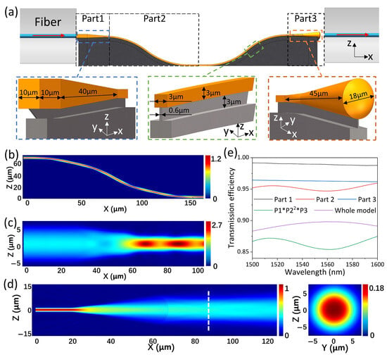
Figure 1.
(a) Rendering diagram of a coupler aligned with single-mode fibers (core in blue), the coupler consists of a smoothly curved stripe waveguide (yellow) and the abutment (gray), which was separated into 3 parts for simulation: square-frustrum waveguide, inverted-S waveguide, and a coupling lens. The insets show a three-dimensional structural diagram of each part of the coupler. (b,c) The electric field distribution of Part2 and Part1 in the X–Z plane, respectively. (d) The electric field distribution of Part3 in the X–Z plane, and the mode field profile at the position indicated by the white dashed line in the main figure. (e) The respective transmittance curves of the 3 parts, whose product is taken as the overall transmittance and that of the whole model simulation.
The transmittance of the optimized one, as shown in Figure 1e, demonstrates that all three parts could achieve more than 94% within a bandwidth of 1.5 μm to 1.6 μm. The product of these individual transmittances was taken as the overall transmission efficiency. To verify the feasibility of the parallel simulation approach, the entire model was simulated, and the results showed a deviation of less than 5% from those obtained via segmented simulation. The discrepancy stems from the continuity of light propagation: in the segmented simulation approach adopted in this study, the input mode of the latter segment does not correspond to the output mode of the former segment, leading to a lack of optical field continuity during light propagation. In contrast, the whole-model simulation preserves continuous light propagation through each segment, thereby maintaining such continuity.
2.2. Fabrication
TPL, a type of LDW technology, offers numerous advantages, including one-step forming, flexible modeling, high machining accuracy [,], capability for massive array fabrication [,], and process visualization, making it suitable for rapid mass fabrication of on-chip devices. And there are various types of photoresins available for TPL, among which IP-n162 is a novel type with a refractive index of about 1.6 and low absorption efficiency in the C-band []. It exhibits an excellent self-smoothing effect during two-photon polymerization. The high refractive index and smooth surface of IP-n162 facilitate coupler miniaturization; thus, the coupler demonstrated in this work was designed based on this photoresin. Figure 2a shows a standard fabrication process for TPL devices, which includes dripping, exposure, and development steps. The substrate used is a ITO glass square with a side length of 25 mm and height of 0.7 mm. Fabrication was performed using a Nanoscribe Photonic Professional GT TPL system, which is equipped with a laser source operating at a wavelength of 780 nm, with a repetition rate of 80 MHz and a pulse width of 120 fs. Coupled with a 25× objective lens with an NA of 0.8, this system achieves a minimum 3D processing linewidth of 350 nm. Moreover, the coupler was modeled using 3D modeling software, with the output saved in a format compatible with photolithography systems.
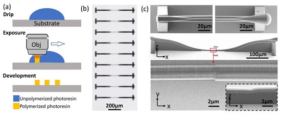
Figure 2.
(a) Diagram of two-photon lithography processing. (b) Optical micrograph of coupler pairs. (c) The SEM micrograph of a coupler pair and the close-up features of its input/output ports and the joint.
In the lithography process, couplers were firstly sliced into a number of layers along the z-direction, using the slicing software Describe (Version 2.7), hatched by the step size of hundreds of nanometers along the light scanning direction, in which the slicing and hatching distances dominate the whole printing time and the fineness of structures. We set the slicing and hatching distances to 0.2 μm and 0.3 μm, which are typical values for 25× objective processing. The voxel aspect ratio was set to 0.2 to create a flat cross-section and prevent adhesion between the waveguide and the abutment. The contour number was set to 0 to reduce the appearance of scale-like structures and to acquire smooth sidewalls, and the printing time of the coupler was about 5 min. The maximum writing field diameter of the 25× objective lens is 400 μm, which is exceeded by the combined length of two couplers, and stitching fabrication is required. The procedure is as follows: Alignment structures were designed at the interface of the two models during the 3D modeling, as shown in the middle inset of Figure 2c. During stitching, the displacement stage was finely adjusted to ensure perfect overlap of these alignment structures. After printing of the devices finished, the substrates were immersed in propylene glycol monomethyl ether acetate (PGMEA) for 15 min and isopropanol (IPA) for 5 min for development and rinsing. Then, they were dried with nitrogen and after by UV lamp to continue to cure for one minute to ensure the mechanical strength. Figure 2b presents optical micrographs of multiple fabricated couplers, demonstrating excellent fabrication uniformity. Figure 2c shows the corresponding SEM image, along with detailed views of the input/output ports and waveguide joints.
2.3. Coupling and Testing
The transmission performance of the coupler was characterized using a fiber input–output system. As illustrated in Figure 3a, a single-mode fiber (SMF) was precisely aligned with the coupler using a five-axis displacement stage, enabling translation along the x-, y-, and z-axes and rotation in the x–y and x–z planes. Figure 3b presents a detailed view of the fiber alignment area, while Figure 3c,d provide top-view and side-view images of the alignment system, respectively. To assess the coupler’s performance in an aqueous environment, the fiber and coupler were first aligned, followed by the controlled dispensing of deionized water onto the ITO substrate to ensure complete immersion of both components.
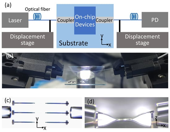
Figure 3.
(a) Schematic diagram of the fiber-coupler alignment system. (b) Physical photo of the fiber-coupler alignment setup. Top-view (c) and side-view (d) micrographs of fibers aligned with the couplers.
We characterized the coupler and its transmission performance using a wavelength-tunable laser that will subsequently be used as the light source for ultrasound detection. This laser has an output wavelength range of 1528–1567 nm, covering the C-band. The input light power is denoted as Pi, and the power transmitted through the coupler is denoted as Pg. Given the structural symmetry of the coupler, particularly the identical designs of Part2 in both coupling sections, the transmittance, t, of a single coupler can be calculated as follows:
3. Results
3.1. Coupling Loss
To validate the robustness of the experimental measurements, nine identical coupler pairs were fabricated on a monolithic ITO substrate through batch processing. As shown in Figure 4a, the broadband transmission performance across 1528–1567 nm was systematically characterized through both spectral analysis and statistical evaluation of nine coupler samples. Each individual device exhibits a broadband transmission loss below −1.3 dB, with a power fluctuation less than 0.2 dB across the operational bandwidth. Notably, the standard deviation of the average transmission loss across the nine couplers remains below 0.25 dB, demonstrating remarkable consistency in fabrication quality and optical performance. And the observed performance discrepancy between the simulation and experimental results is primarily attributed to the following three synergistic factors: (1) submicron-scale fabrication tolerances inherent to laser direct writing processes, (2) micrometer-level surface roughness at waveguide interfaces, and (3) manual assembly misalignments in critical dimensions. These fabrication-induced variations, as corroborated by the SEM morphological characterization shown in Figure 2c, collectively contribute to the deviation in transmission efficiency between theoretical predictions and empirical measurements.
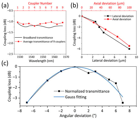
Figure 4.
(a) Broadband transmission performance (1528–1567 nm) with statistical evaluation of nine couplers, showing an average transmittance better than −1.3 dB and a standard deviation less than 0.25 dB. (b) The lateral and axial deviations of the coupler. (c) The angular misalignment tolerance of the coupler, revealing performance boundaries of ±3° (−1 dB) and ±6° (−3 dB) through Gaussian-fitted experimental data.
Fiber alignment tolerance represents a critical parameter for practical deployment. To systematically quantify this effect, we characterized the coupling efficiency at 1550 nm under the following three misalignment scenarios: lateral (y-direction) displacement, axial (x-direction) displacement, and angular deviation (rotation about the y-axis). As shown in Figure 4b, the −1 dB tolerance thresholds were measured as 2.5 μm (lateral) and 20 μm (axial), respectively. Angular misalignment analysis, as shown in Figure 4c with Gaussian fitting curves, revealed tolerance ranges of ±3° for a −1 dB transmission loss and ±6° for a −3 dB degradation. These findings demonstrate the coupler’s robustness against alignment variations while establishing quantitative benchmarks for optical system integration.
3.2. Ultrasound Detection
The coupler was originally designed to integrate with on-chip resonators, enabling ultrasound detection in liquid environments. To validate this functionality, we implemented a phase-shifted Bragg-grating (PS-BG) array on an ITO substrate. The fabrication of PS-BGs requires a processing resolution of approximately 200 nm (one-tenth of the grating period). The 25× objective lens used for coupler fabrication cannot meet this requirement, and the self-smoothing effect of IP-n162 photoresin results in unsharp grating teeth, thus rendering the coupler processing system unsuitable for grating fabrication. To address this, the present study employs a combination of IP-Dip photoresin and a 63× objective lens for grating fabrication. After two-photon curing, IP-Dip exhibits a refractive index of approximately 1.53 at the 1550 nm band [,]. With the 63× objective lens featuring a numerical aperture of 1.4, this combination achieves a three-dimensional processing accuracy of less than 200 nm, whose processing parameters meet the fabrication criteria for PS-BGs.
The PS-BG features a total length of 200 μm, cross-sectional dimensions of 3 μm × 3 μm, a period of 2.1 μm, a duty cycle of 0.6, and a corrugation depth of 1 μm. To achieve ultra-fine fabrication, the slicing distance and hatching distance were set to 0.1 μm and 0.05 μm, respectively. Two sets of alignment structures were designed to interface with the input and output couplers. After the grating fabrication and development process, IP-n162 photoresin was dispensed to proceed with the fabrication of the couplers. The fabricated device’s structure is shown in Figure 5a. After the input and output optical fibers were aligned with the coupler, as shown in Figure 3, ultraviolet (UV) curing adhesive was used to fix the fibers onto the ITO glass. It should be noted here that the UV adhesive must not cover the coupler or the phase-shifted grating.
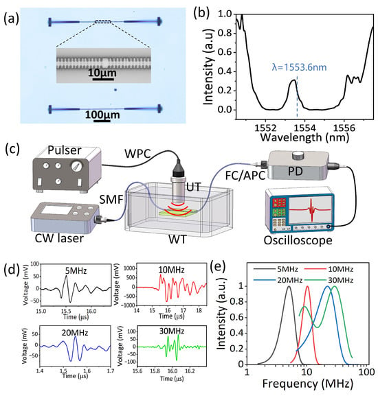
Figure 5.
(a) Optical micrograph of PS-BGs connecting to couplers; the inset shows a close-up SEM of the Bragg grating. (b) Transmission spectrum of the π-BG. The resonance peak appears near 1553.5 nm. (c) The schematic diagram of the PS-BG ultrasound detection system. (d) The time-domain signals of the PS-BG ultrasound detector for 5 MHz, 10 MHz, 20 MHz, and 30 MHz transducers, and (e) shows the frequency spectra of the 5–30 MHz time-signals in (d), for which the frequency responses at 5 MHz and 10 MHz correspond exactly to their transducers’ spectra. WPC: waterproof cable; WT: water tank; UT: ultrasound transducer; SMF: single-mode fiber.
After completing the coupling between the optical fiber and the grating, the assembly was immersed in water to measure the transmission spectrum of the grating, as shown in Figure 5b. It can be observed that the resonance wavelength was 1553.5 nm, corresponding to a quality factor of 3107. Subsequently, the ultrasound detection system, illustrated in Figure 5c, was constructed. The output wavelength of the CW laser was tuned to the position of the maximum slope of the resonance peak (1553.6 nm) to achieve high-sensitivity detection. Ultrasound transducers with central frequencies of 5, 10, 20, and 30 MHz were used as ultrasound sources to test the ultrasonic response of the PS-BG. Figure 5d presents the time-domain response waveforms of the PS-BG to each ultrasound frequency, with corresponding signal-to-noise ratios (SNRs) of 13.4 dB, 13.2 dB, 11.8 dB, and 15.9 dB, respectively. Fourier transform of each time-domain signal yielded the frequency-domain information of the PS-BG, as shown in Figure 5e, which reveals a detection fidelity within 5–30 MHz for the PS-BG, while simultaneously demonstrating the coupler’s capability to maintain stable optical transmission under ultrasound-induced perturbations in aqueous conditions.
4. Conclusions and Discussion
We present a compact fiber-chip coupler (250 μm × 20 μm × 75 μm) specifically designed for on-chip all-optical ultrasound detection. The device is fabricated using two-photon polymerization 3D printing technology, with each coupler requiring only 5 min of fabrication time. Batch processing of coupler arrays could further enhance production efficiency. In aqueous environments, the coupler demonstrates stable optical performance with a broadband transmission loss below −1.3 dB (1528–1567 nm) and power fluctuations under 0.2 dB. Its alignment tolerance meets practical requirements, as follows: lateral (2.5 μm) and axial (20 μm) displacements at −1 dB loss, along with a ±3° angular deviation tolerance. The measured 0.25 dB standard deviation in transmission efficiency across nine couplers confirms the fabrication consistency.
After integration with an on-chip PS-BG, the system successfully detects 5–30 MHz ultrasound signals with high-frequency fidelity. Additionally, it is compatible with various material substrates. For example, when integrated with all-optical ultrasound detectors based on transparent glass substrates, it allows coaxial excitation and detection of photoacoustic signals, thereby simplifying the structure of such new imaging systems. Based on the above, this coupler holds promising applications in all-optical ultrasound detection, biomedical photoacoustic imaging, and industrial non-destructive testing.
Author Contributions
Conceptualization, C.Z. (Chonglei Zhang) and C.Z. (Chao Zhao); methodology, software, validation, writing—original draft preparation, and data curation, C.Z. (Chao Zhao); visualization and writing—review and editing, C.Z. (Chao Zhao) and P.L. All authors have read and agreed to the published version of the manuscript.
Funding
This research was funded by the National Nature Science Foundation of China, grant number 91850202, and the State Key Laboratory of Radio Frequency Heterogeneous Integration, Independent Scientific Research Program No. 2024002.
Acknowledgments
The authors express gratitude to the Photonics Center of Shenzhen University for devices machining.
Conflicts of Interest
The authors declare that they have no known competing financial interests or personal relationships that could have appeared to influence the work reported in this paper.
References
- Cao, X.; Yang, H.; Wu, Z.-L.; Li, B.-B. Ultrasound sensing with optical microcavities. Light Sci. Appl. 2024, 13, 159. [Google Scholar] [CrossRef]
- Shnaiderman, R.; Wissmeyer, G.; Ulgen, O.; Mustafa, Q.; Chmyrov, A.; Ntziachristos, V. A submicrometre silicon-on-insulator resonator for ultrasound detection. Nature 2020, 585, 372–378. [Google Scholar] [CrossRef] [PubMed]
- Hazan, Y.; Levi, A.; Nagli, M.; Rosenthal, A. Silicon-photonics acoustic detector for optoacoustic micro-tomography. Nat. Commun 2022, 13, 1488. [Google Scholar] [CrossRef]
- Liang, Y.; Fu, W.; Li, Q.; Chen, X.; Sun, H.; Wang, L.; Jin, L.; Huang, W.; Guan, B.-O. Optical-resolution functional gastrointestinal photoacoustic endoscopy based on optical heterodyne detection of ultrasound. Nat. Commun. 2022, 13, 7604. [Google Scholar] [CrossRef] [PubMed]
- Nagli, M.; Koch, J.; Hazan, Y.; Volodarsky, O.; Ravi Kumar, R.; Levi, A.; Hahamovich, E.; Ternyak, O.; Overmeyer, L.; Rosenthal, A. Silicon-photonics focused ultrasound detector for minimally invasive optoacoustic imaging. Biomed. Opt. Express 2022, 13, 6229–6244. [Google Scholar] [CrossRef] [PubMed]
- Ding, Z.; Sun, J.; Li, C.; Shi, Y. Broadband Ultrasound Detection Using Silicon Micro-Ring Resonators. J. Light. Technol. 2023, 41, 1906–1910. [Google Scholar] [CrossRef]
- Nagli, M.; Moisseev, R.; Suleymanov, N.; Kaminski, E.; Hazan, Y.; Gelbert, G.; Goykhman, I.; Rosenthal, A. Silicon photonic acoustic detector (SPADE) using a silicon nitride microring resonator. Photoacoustics 2023, 32, 100527. [Google Scholar] [CrossRef]
- Pan, J.; Li, Q.; Feng, Y.; Zhong, R.; Fu, Z.; Yang, S.; Sun, W.; Zhang, B.; Sui, Q.; Chen, J.; et al. Parallel interrogation of the chalcogenide-based micro-ring sensor array for photoacoustic tomography. Nat. Commun. 2023, 14, 3250. [Google Scholar] [CrossRef]
- Sun, J.; Tang, S.-J.; Meng, J.-W.; Li, C. Whispering-gallery optical microprobe for photoacoustic imaging. Photonics Res. 2023, 11, A65–A71. [Google Scholar] [CrossRef]
- Yang, L.; Xu, D.; Chen, G.; Wang, A.; Li, L.; Sun, Q. Miniaturized fiber optic ultrasound sensor with multiplexing for photoacoustic imaging. Photoacoustics 2022, 28, 100421. [Google Scholar] [CrossRef]
- Ma, J.; Zhao, J.; Chen, H.; Sun, L.-P.; Li, J.; Guan, B.-O. Transparent microfiber Fabry-Perot ultrasound sensor with needle-shaped focus for multiscale photoacoustic imaging. Photoacoustics 2023, 30, 100482. [Google Scholar] [CrossRef]
- Wei, H.; Wu, Z.; Sun, K.; Zhang, H.; Wang, C.; Wang, K.; Yang, T.; Pang, F.; Zhang, X.; Wang, T.; et al. Two-photon 3D printed spring-based Fabry–Pérot cavity resonator for acoustic wave detection and imaging. Photonics Res. 2023, 11, 780–786. [Google Scholar] [CrossRef]
- Wei, H.; Wei, Y.; Zhuang, C.; He, G.; Yang, T.; Zhang, X.; Pang, F.; Wang, T.; Krishnaswamy, S.; Caucheteur, C.; et al. Sensitivity-Enhanced Fiber-Optic Fabry–Perot Ultrasonic Sensor Based on Direct Laser Writing of Dual-Resonant Cavity. IEEE Trans. Instrum. Meas. 2025, 74, 1–6. [Google Scholar] [CrossRef]
- He, A.; Guo, X.; Wang, T.; Su, Y. Ultracompact Fiber-to-Chip Metamaterial Edge Coupler. ACS Photonics 2021, 8, 3226–3233. [Google Scholar] [CrossRef]
- Ying, P.; Tan, H.; Zhang, J.; He, M.; Xu, M.; Liu, X.; Ge, R.; Zhu, Y.; Liu, C.; Cai, X. Low-loss edge-coupling thin-film lithium niobate modulator with an efficient phase shifter. Opt. Lett. 2021, 46, 1478–1481. [Google Scholar] [CrossRef]
- Chen, H.; Ma, F.; Chen, K.; Dong, J. An Ultrabroadband and Cost-Effective Edge Coupler for Efficient Thin Film Lithium Niobate Photonics. Photonics 2023, 10, 760. [Google Scholar] [CrossRef]
- Marchetti, R.; Lacava, C.; Khokhar, A.; Chen, X.; Cristiani, I.; Richardson, D.J.; Reed, G.T.; Petropoulos, P.; Minzioni, P. High-efficiency grating-couplers: Demonstration of a new design strategy. Sci. Rep. 2017, 7, 16670. [Google Scholar] [CrossRef] [PubMed]
- Chen, B.; Ruan, Z.; Fan, X.; Wang, Z.; Liu, J.; Li, C.; Chen, K.; Liu, L. Low-loss fiber grating coupler on thin film lithium niobate platform. APL Photonics 2022, 7, 076103. [Google Scholar] [CrossRef]
- Gehring, H.; Blaicher, M.; Hartmann, W.; Varytis, P.; Busch, K.; Wegener, M.; Pernice, W.H.P. Low-loss fiber-to-chip couplers with ultrawide optical bandwidth. APL Photonics 2019, 4, 010801. [Google Scholar] [CrossRef]
- Gehring, H.; Eich, A.; Schuck, C.; Pernice, W.H.P. Broadband out-of-plane coupling at visible wavelengths. Opt. Lett. 2019, 44, 5089–5092. [Google Scholar] [CrossRef]
- Hartmann, W.; Varytis, P.; Gehring, H.; Walter, N.; Beutel, F.; Busch, K.; Pernice, W. Waveguide-Integrated Broadband Spectrometer Based on Tailored Disorder. Adv. Opt. Mater. 2020, 8, 1901602. [Google Scholar] [CrossRef]
- Huang, S.-W.; Chen, S.-L.; Ling, T.; Maxwell, A.; O’Donnell, M.; Guo, L.J.; Ashkenazi, S. Low-noise wideband ultrasound detection using polymer microring resonators. Appl. Phys. Lett. 2008, 92, 193509. [Google Scholar] [CrossRef]
- Ling, T.; Chen, S.-L.; Guo, L.J. High-sensitivity and wide-directivity ultrasound detection using high Q polymer microring resonators. Appl. Phys. Lett. 2011, 98, 204103. [Google Scholar] [CrossRef]
- Dong, B.; Chen, S.; Zhang, Z.; Sun, C.; Zhang, H.F. Photoacoustic probe using a microring resonator ultrasonic sensor for endoscopic applications. Opt Lett 2014, 39, 4372–4375. [Google Scholar] [CrossRef]
- Zhang, C.; Chen, S.L.; Ling, T.; Guo, L.J. Imprinted Polymer Microrings as High-Performance Ultrasound Detectors in Photoacoustic Imaging. J. Light. Technol. 2015, 33, 4318–4328. [Google Scholar] [CrossRef]
- Witzgall, G.; Vrijen, R.; Yablonovitch, E.; Doan, V.; Schwartz, B.J. Single-shot two-photon exposure of commercial photoresist for the production of three-dimensional structures. Opt. Lett. 1998, 23, 1745–1747. [Google Scholar] [CrossRef] [PubMed]
- Bentley, S.J.; Boyd, R.W. Nonlinear optical lithography with ultra-high sub-Rayleigh resolution. Opt. Express 2004, 12, 5735–5740. [Google Scholar] [CrossRef]
- Faraji Rad, Z.; Prewett, P.D.; Davies, G.J. High-resolution two-photon polymerization: The most versatile technique for the fabrication of microneedle arrays. Microsyst. Nanoeng. 2021, 7, 71. [Google Scholar] [CrossRef] [PubMed]
- Cao, C.; Qiu, Y.; Guan, L.; Wei, Z.; Yang, Z.; Zhan, L.; Zhu, D.; Ding, C.; Shen, X.; Xia, X.; et al. Dip-In Photoresist for Photoinhibited Two-Photon Lithography to Realize High-Precision Direct Laser Writing on Wafer. ACS Appl. Mater. Interfaces 2022, 14, 31332–31342. [Google Scholar] [CrossRef]
- Aderneuer, T.; Fernández, O.; Ferrini, R. Two-photon grayscale lithography for free-form micro-optical arrays. Opt. Express 2021, 29, 39511–39520. [Google Scholar] [CrossRef]
- McKee, S.; Lutey, A.; Sciancalepore, C.; Poli, F.; Selleri, S.; Cucinotta, A. Microfabrication of polymer microneedle arrays using two-photon polymerization. J. Photochem. Photobiol. B Biol. 2022, 229, 112424. [Google Scholar] [CrossRef] [PubMed]
- Schmid, M.; Ludescher, D.; Giessen, H. Optical properties of photoresists for femtosecond 3D printing: Refractive index, extinction, luminescence-dose dependence, aging, heat treatment and comparison between 1-photon and 2-photon exposure. Opt. Mater. Express 2019, 9, 4564–4577. [Google Scholar] [CrossRef]
- Dottermusch, S.; Busko, D.; Langenhorst, M.; Paetzold, U.W.; Richards, B.S. Exposure-dependent refractive index of Nanoscribe IP-Dip photoresist layers. Opt. Lett. 2019, 44, 29–32. [Google Scholar] [CrossRef] [PubMed]
Disclaimer/Publisher’s Note: The statements, opinions and data contained in all publications are solely those of the individual author(s) and contributor(s) and not of MDPI and/or the editor(s). MDPI and/or the editor(s) disclaim responsibility for any injury to people or property resulting from any ideas, methods, instructions or products referred to in the content. |
© 2025 by the authors. Licensee MDPI, Basel, Switzerland. This article is an open access article distributed under the terms and conditions of the Creative Commons Attribution (CC BY) license (https://creativecommons.org/licenses/by/4.0/).