Abstract
Optical phase control is essential for optical beam steering applications. The silicon nitride thermo-optic modulator generally suffers from high electrical power consumption. Microresonator and multipass structures could reduce the electrical power consumption of silicon nitride thermo-optic modulators, with the drawback of a narrow operating bandwidth and high insertion loss. We demonstrate a single-pass silicon nitride thermo-optic phase modulator at 532 nm with low insertion loss and low power consumption, achieving a π phase shift power consumption down to 0.63 mW in a Mach–Zehnder switch. The rise and fall time are around 1.07 ms and 0.67 ms, respectively.
1. Introduction
Integrated photonics in the visible spectrum holds significance for a variety of emerging applications, such as augmented- and virtual-reality displays [1,2], quantum information processing [3,4], nonlinear optics [5,6], optical sensing [7,8], and optogenetics [9,10]. The large-scale integration of phase modulators is at the core of photonic systems for on-chip optical routing and free-space wavefront shaping, two fundamental operations that are crucial to the achievement of the aforementioned applications at telecom, as well as visible, wavelengths [11,12]. Light can be routed toward different output ports by means of constructive and destructive interference between different waveguides.
Complementary metal-oxide-semiconductor (CMOS) process-compatible material platforms for visible-spectrum integrated photonics, such as silicon nitride (SiNx) [9,13,14,15,16,17,18,19,20], aluminum nitride (AlN) [5,21,22], and silicon dioxide (SiO2) [23,24], exhibit relatively weak thermo-optic (TO) and almost nonexistent electro-optic (EO) effects. In particular, the TO coefficient of SiNx is significantly smaller than that of silicon [25]. In the case of TO modulators based on SiNx, the typical power required for phase tuning, denoted as P(π), is in the tens of milliwatts (mW) range at visible wavelengths [2,10]. This level of power consumption is not scalable for large arrays for optoelectronic devices. To reduce power consumption, one strategy is to use a resonant cavity as a phase modulator, which reduces power consumption to the order of mW, but has the drawback of narrow band operation and low fabrication tolerance [11]. Another strategy is to use a suspended structure, which can result in significantly lower power consumption, as reported by several groups [26,27]. An integrated multipass strategy with a suspended structure can achieve sub-milliwatt operation at a shorter wavelength, with the drawback of high insertion loss and crosstalk between spiral waveguides [26]. To enhance the performance of modulators, emerging two-dimensional (2D) materials [27,28] (Ref: Nature Reviews Materials 8, 498–517, 2023) have demonstrated excellent performance in thermal-optic modulation. However, the complex preparation and transfer processes of 2D materials also face the challenge of low yield in practical PIC applications. In order to achieve better modulation rates, lithium niobate electro-optic modulators have shown low loss and ultra-high-speed characteristics in the C-band, but, due to processing difficulties and high costs, they cannot be widely applied on a large scale [29]. We compared the performance of our proposed phase modulator with the state-of-the-art TO SiNx modulators in visible-spectrum devices developed in recent years, as shown in Table 1.

Table 1.
Performance of the SiNx modulator for the visible spectrum.
In this wok, we optimized the suspended TO phase modulator and demonstrated a power-efficient, high-performance suspended TO modulator on a high-confinement SiNx waveguide platform at green wavelengths (λ = 532 nm). We achieved a π phase shift in power consumption down to 0.63 mW in a Mach–Zehnder interferometer (MZI) with a rise and fall time of around 1.07 ms and 0.67 ms, respectively.
2. Design and Simulations
Our SiNx suspended MZI is shown schematically in Figure 1a. It was designed on a silicon substrate with a 3 μm thermal silicon oxide layer and a SiNx thickness of 180 nm. The top-view and cross-section schematics of the proposed phase modulator are shown in Figure 1b,c, respectively. The MZI structure is used to measure the TO tuning performance of the phase modulator with NiCr heating resistors, connected by gold wiring and bonding pads. The waveguide width is 300 nm. The width of the suspended SiO2 waveguide beam is w, while a window of length p and spacing d is cut through the silicon oxide in order to further etch the substrate below the waveguide. The spacing d serves as the supporting arm that connects the suspended waveguide beam to the surrounding structure.
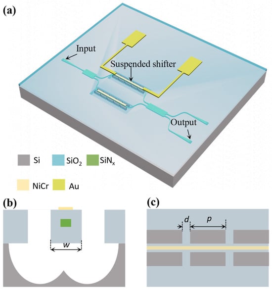
Figure 1.
(a) The 3D schematic of the suspended MZI. (b) The cross-section diagram of the suspended phase modulator. w—the width of the suspended SiO2 waveguide beam. (c) The surface diagram of the suspended phase modulator. p—length of window and d—spacing between the windows.
We carried out a series of simulations to assess the impact of various structural parameters on TO tuning performance and structural stability, as presented in Table 2. When comparing Device 1 with Device 2, we observed a drastic drop in the power consumption by reducing the suspended opening window spacing (d). A smaller d resulted in a much lower power consumption for the phase modulator. This can be attributed to the fact that in the suspended region, heat is primarily transferred away via the silicon oxide support arms. Reducing d corresponds to a reduced rate of heat transfer. We set d to 2 μm, which maintains a low power consumption with an acceptable fabrication tolerance.
Table 2.
The power consumption Pπ and the maximum stress σ and deformation Δ of the suspended modulator with respect to the structural parameters at a waveguide temperature rise of 42.7°.
To further reduce the power consumption of the phase shifter, we reduced the cross-sectional area of the heated waveguide beam section by reducing w from 12 μm (Device 2) to 8 μm (Device 3), which reduced the total thermal capacitance of the heated section. A minimum w of 8 μm was used to ensure efficient waveguide transmission while maintaining structural stability and an acceptable tolerance of alignment errors between different layers.
A comparison was performed between the effects of different window lengths (P) on TO tuning performance and structural stability, shown as Device 3 through Device 7. In this analysis, the phase modulator structures were categorized into five types, each covered with windows of varying lengths: 50 µm, 80 µm, 100 µm, 150 µm, and 300 µm, respectively. Longer windows (and, hence, fewer supporting arms) resulted in a lower power consumption for the device. Although this improvement comes with the drawback of an increased danger of stress and deformation, this deformation is a maximum of only 63 nm, with a maximum stress of 1.6 × 10⁸ Pa, which is much smaller than the allowable stress (1.34 × 10⁹ Pa) for silica [31].
Figure 2 shows the simulated temperature distribution, stress distribution, and deformation distribution for the suspended region based on the finite element method (FEM), respectively. The thermal convection coefficient of air is assumed to be 5 W·m−2·K−1 [12], while the thermal conduction coefficient of SiNx is considered to be 2.45 × 10⁵ W·m−2·K−1 [25], and the room temperature is set at 300 K. This analysis reveals that the temperature of the waveguide core could potentially increase to 360 K. The phase tuning as a function of temperature variation can be expressed as [12]
where λ0 is the free-space wavelength, L is the heating length, and is the variation in the effective refractive index of the waveguide. Therefore, for a 300 µm-long waveguide phase modulator, as the temperature of the waveguide increases from 300 K to 342.7 K (corresponding to Table 2), the effective refractive index increases by 8.8 × 10⁻⁴. Figure 2a,b depict the simulated temperature distribution of Device 1 and Device 7 when the average temperature of the waveguide is elevated by 42.7 °C. This temperature rise is expected to result in a phase shift of . The figures illustrate lower waveguide temperatures around the supporting arms, confirming that the primary route of heat dissipation is via the support arms of the silicon oxide to the surrounding environment. This observation explains why reducing both ‘p’ and ‘d’ can effectively diminish power consumption. Figure 2c,d depict the stress distribution in Device 1 and Device 7, with minimal observable differences. In Figure 2e,f, the thermal deformation distribution of these two devices is presented, primarily concentrated in the suspended sections. Device 1 exhibits a maximum deformation of 2.1 nm, whereas Device 7 experiences a more significant deformation of 63 nm. The maximum deformation is within 0.02% of the waveguide length. The optical effects induced by this waveguide bending are considered negligible.

Figure 2.
Device 1 (a,c,e) and Device 7 (b,d,f) when the average temperature of the waveguide increases by 42.7 °C. (a,b) Temperature distribution; (c,d) stress distribution; and (e,f) the distribution of deformation.
3. Chip Fabrication
To fabricate the suspended MZI, the process began with the deposition of 180 nm of our proprietary [32,33] (Figure 3a) inductively coupled plasma chemical vapour deposition (ICPCVD) SiNx on a silicon substrate layered with 3 µm of thermal silicon oxide, as presented in Figure 3b. Subsequently, the pattern was defined by means of electron beam lithography (EBL) and transferred into the SiNx layer via reactive ion etching (RIE), as depicted in Figure 3c.
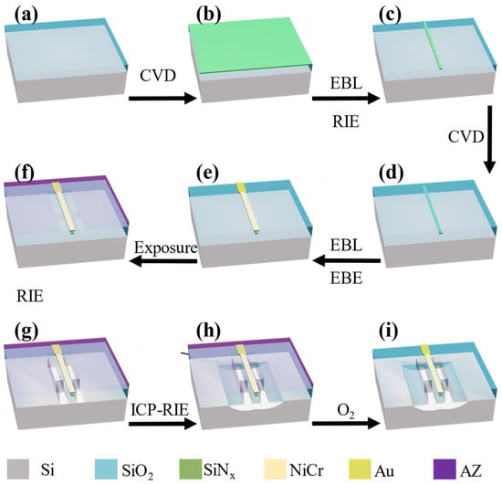
Figure 3.
Manufacturing process of the suspended phase modulator. CVD: Chemical Vapor Deposition; EBL: Electron Beam Lithography; RIE: Reactive Ion Etching; EBE: Electron Beam Evaporation; ICP-RIE: Inductively Coupled Plasma-Reactive Ion Etching.
Following the etching, the waveguides were coated with 600 nm of PECVD oxide, as indicated in Figure 3d. To pattern the switch, a metal lift-off process was employed to define layers of 200 nm of NiCr and 600 nm of Au, as shown in Figure 3e. Utilizing a 4 µm thick photoresist, an etch mask was created to safeguard the silicon oxide cladding, leaving the silicon etching window regions exposed, as displayed in Figure 3f. The silicon oxide cladding in these window regions were selectively removed using reactive ion etching (RIE), as illustrated in Figure 3g. Finally, the suspended structure was achieved by executing a series of undercut etching processes, resulting in deep trenches etched into the Si substrate, as shown in Figure 3h. The remaining photoresist was removed using O2 plasma, as demonstrated in Figure 3i. For characterization, the MZI chip was wire-bonded to a printed circuit board (PCB).
In Figure 4a, a microscope image of the suspended phase modulators is presented, wherein both arms of the MZI structure are coated with NiCr films and suspended to achieve loss equilibrium. Gold (Au) deposition is carried out on both of the MZI tuning arms for connection to the PCB. The NiCr layer covering the cladding above the waveguide extends 300 µm along the waveguide. A pair of grating couplers designed for TE polarization are used to couple with the input/output fibers. To provide further insight, a scanning electron microscope (SEM) image illustrating the cross-section of the phase modulator is shown in Figure 4b. The cross-sectional area of the suspended section measures 12 μm × 3.8 μm (width × height), including the 8 μm wide windows on both sides. The isotropic etching of the silicon substrate is carried out through the 20 μm deep window.
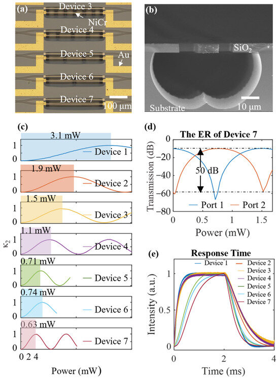
Figure 4.
(a) Microscope photograph of a representative device. (b) SEM photograph of a cross-section of a suspended structure. (c) The tested Pπ of Devices P1 and P2 are the optical power of the two output ports of the MZI κ2 = P2/(P1 + P2). (d) The extinction ratio for Device 7. (e) The tested response time of devices at λ = 532 nm.
4. Chip Characterization
The measured interference characteristics of Devices 1–7 at λ = 532 nm versus the heating power applied to one of the arms are shown in Figure 4c. Device 7 exhibits a reduction by a factor of 5 in terms of power consumption compared with Device 1, achieving a half-wave power of only 0.63 mW compared to 3.1 mW with the same waveguide parameters. The test results for Devices 1–5 are more consistent with the simulated structure and verify that the power consumption of the phase modulator decreases as the length of the open window increases. The power consumption of Devices 6–7 is slightly higher than in the simulation. In Figure 4d, we show the plot of the optical power as a function of the heating power for the two ports of Device 7, where an extinction ratio of 50 dB is demonstrated. The MZI insertion loss of the device was measured as ~9 dB, which included the coupling loss, transmission loss, and excess loss. The primary optical losses within the structure are due to coupling between the fiber and the chip and propagation losses through the waveguides. Regarding the coupling loss, in this preliminary demonstration, the mode mismatch between the fiber and the input grating resulted in a coupling loss of about 4.1 dB. Similarly, our propagation losses were of approximately 3 dB/cm.
The modulation speed of the devices was measured by applying a square wave to the microheater and monitoring the output from one port of the devices. As shown in Figure 4e, the time constants of the rising and falling edges of the signals are extracted by fitting the 10−90% portion of the edges to an exponential function. The response times are 0.33 ms (rising) and 0.69 ms (falling) for Device 1, with 1.07 ms (rising) and 0.67 ms (falling) for Device 7, respectively.
Essentially, the low and slower response time result from the better thermal insulation that comes with fewer support arms and smaller suspended structures. The slower speed is a potential disadvantage for the suspended phase modulators with a longer window. However, many applications in the visible range, unlike in telecommunications, do not require very high modulation speeds. For example, optogenetic probes only need to fire faster than neurons (which typically fire at a few hundred Hertz), and atomic trapping is a near-static scenario [30].
We conducted a comparative study of 34 suspended MZI devices and 8 conventional MZI devices manufactured on the same chip. These two types of devices had the same grating coupler, MZI, and microheater, except that the suspended MZI opens a specific size of silicon dioxide window and excavates the silicon substrate. After testing, the light at 532 nm had a loss of about 10 dB across all devices, and the suspended structure or fewer-support-arm structures did not show a greater insertion loss. Unfortunately, there were two suspended MZIs (Device 2 and Device 5) and one conventional MZI microheater that had no resistance when measured with a multimeter. This may be caused by the partial metal fracture during electron beam evaporation (EBE) deposition.
Our research shows that the suspended MZI devices have good repeatability during the manufacturing process, showing similar performance and characteristics. This indicates that our manufacturing process has excellent control capabilities and can achieve consistent performance between different devices. After 5 months of testing, our suspended MZI devices still maintain good working condition. This indicates that the devices have long-term stability and reliability.
5. Conclusions
In conclusion, we minimize the power consumption of the suspended TO phase modulator and demonstrate an extremely power efficient high-performance TO modulator at green wavelengths (λ = 532 nm). Fabricated using a CMOS-compatible SiNx platform, the device achieves a π phase shift power consumption down to 0.63 mW and an extinction ratio over 50 dB in an MZI, respectively. Thus, our work not only demonstrates a highly efficient extinction ratio phase modulator, but also offers a new design pathway for optical modulation devices in large-scale PICs.
Author Contributions
Z.W. led the experiments with assistance from S.L. Z.W. designed and fabricated the SiNx MZI devices. Y.Z. and S.Y. prepared the manuscript. All authors have read and agreed to the published version of the manuscript.
Funding
This research was funded by National Natural Science Foundation of China (NSFC) (61975243, 62335019); Science and Technology Program of Guangzhou (202103030001).
Institutional Review Board Statement
The study did not require ethical approval.
Informed Consent Statement
The study did not involve humans.
Data Availability Statement
The data underlying the results presented in this paper are not publicly available at this time but may be obtained from the authors upon reasonable request.
Conflicts of Interest
The authors declare no conflicts of interest.
References
- Raval, M.; Yaacobi, A.; Watts, M.R. Integrated Visible Light Phased Array System for Autostereoscopic Image Projection. Opt. Lett. 2018, 43, 3678–3681. [Google Scholar] [CrossRef]
- Chul Shin, M.; Mohanty, A.; Watson, K.; Bhatt, G.R.; Phare, C.T.; Miller, S.A.; Zadka, M.; Lee, B.S.; Ji, X.; Datta, I.; et al. Chip-Scale Blue Light Phased Array. Opt. Lett. 2020, 45, 1934–1937. [Google Scholar] [CrossRef]
- Sipahigil, A.; Evans, R.E.; Sukachev, D.D.; Burek, M.J.; Borregaard, J.; Bhaskar, M.K.; Nguyen, C.T.; Pacheco, J.L.; Atikian, H.A.; Meuwly, C.; et al. An Integrated Diamond Nanophotonics Platform for Quantum-Optical Networks. Science (1979) 2016, 354, 847–850. [Google Scholar] [CrossRef]
- Mehta, K.K.; Bruzewicz, C.D.; McConnell, R.; Ram, R.J.; Sage, J.M.; Chiaverini, J. Integrated Optical Addressing of an Ion Qubit. Nat. Nanotechnol. 2016, 11, 1066–1070. [Google Scholar] [CrossRef] [PubMed]
- Moss, D.J.; Morandotti, R.; Gaeta, A.L.; Lipson, M. New CMOS-Compatible Platforms Based on Silicon Nitride and Hydex for Nonlinear Optics. Nat. Photonics 2013, 7, 597–607. [Google Scholar] [CrossRef]
- Xiong, C.; Pernice, W.H.P.; Sun, X.; Schuck, C.; Fong, K.Y.; Tang, H.X. Aluminum Nitride as a New Material for Chip-Scale Optomechanics and Nonlinear Optics. New J. Phys. 2012, 14, 095014. [Google Scholar] [CrossRef]
- Armani, A.M.; Kulkarni, R.P.; Fraser, S.E.; Flagan, R.C.; Vahala, K.J. Label-Free, Single-Molecule Detection with Optical Microcavities. Science (1979) 2007, 317, 783–787. [Google Scholar] [CrossRef]
- Zhu, J.; Ozdemir, S.K.; Xiao, Y.-F.; Li, L.; He, L.; Chen, D.-R.; Yang, L. On-Chip Single Nanoparticle Detection and Sizing by Mode Splitting in an Ultrahigh-Q Microresonator. Nat. Photonics 2010, 4, 46–49. [Google Scholar] [CrossRef]
- Hoffman, L.; Subramanian, A.; Helin, P.; Bois, B.D.; Baets, R.; Van Dorpe, P.; Gielen, G.; Puers, R.; Braeken, D. Low Loss CMOS-Compatible PECVD Silicon Nitride Waveguides and Grating Couplers for Blue Light Optogenetic Applications. IEEE Photonics J. 2016, 8, 1–11. [Google Scholar] [CrossRef]
- Mohanty, A.; Li, Q.; Tadayon, M.A.; Roberts, S.P.; Bhatt, G.R.; Shim, E.; Ji, X.; Cardenas, J.; Miller, S.A.; Kepecs, A.; et al. Reconfigurable Nanophotonic Silicon Probes for Sub-Millisecond Deep-Brain Optical Stimulation. Nat. Biomed. Eng. 2020, 4, 223–231. [Google Scholar] [CrossRef]
- Liang, G.; Huang, H.; Mohanty, A.; Shin, M.C.; Ji, X.; Carter, M.J.; Shrestha, S.; Lipson, M.; Yu, N. Robust, Efficient, Micrometre-Scale Phase Modulators at Visible Wavelengths. Nat. Photonics 2021, 15, 908–913. [Google Scholar] [CrossRef]
- Tong, W.; Yang, E.; Pang, Y.; Yang, H.; Qian, X.; Yang, R.; Hu, B.; Dong, J.; Zhang, X. An Efficient, Fast-Responding, Low-Loss Thermo-Optic Phase Shifter Based on a Hydrogen-Doped Indium Oxide Microheater. Laser Photon Rev. 2023, 17, 2201032. [Google Scholar] [CrossRef]
- Romero-García, S.; Merget, F.; Zhong, F.; Finkelstein, H.; Witzens, J. Silicon Nitride CMOS-Compatible Platform for Integrated Photonics Applications at Visible Wavelengths. Opt. Express 2013, 21, 14036. [Google Scholar] [CrossRef]
- Shim, E.; Chen, Y.; Masmanidis, S.; Li, M. Multisite Silicon Neural Probes with Integrated Silicon Nitride Waveguides and Gratings for Optogenetic Applications. Sci. Rep. 2016, 6, 22693. [Google Scholar] [CrossRef] [PubMed]
- Poulton, C.V.; Byrd, M.J.; Raval, M.; Su, Z.; Li, N.; Timurdogan, E.; Coolbaugh, D.; Vermeulen, D.; Watts, M.R. Large-Scale Silicon Nitride Nanophotonic Phased Arrays at Infrared and Visible Wavelengths. Opt. Lett. 2017, 42, 21–24. [Google Scholar] [CrossRef] [PubMed]
- Shah Hosseini, E.; Yegnanarayanan, S.; Atabaki, A.H.; Soltani, M.; Adibi, A. High Quality Planar Silicon Nitride Microdisk Resonators for Integrated Photonics in the Visible Wavelength Range. Opt. Express 2009, 17, 14543. [Google Scholar] [CrossRef]
- Sacher, W.D.; Luo, X.; Yang, Y.; Chen, F.-D.; Lordello, T.; Mak, J.C.C.; Liu, X.; Hu, T.; Xue, T.; Guo-Qiang Lo, P.; et al. Visible-Light Silicon Nitride Waveguide Devices and Implantable Neurophotonic Probes on Thinned 200 mm Silicon Wafers. Opt. Express 2019, 27, 37400. [Google Scholar] [CrossRef]
- Gorin, A.; Jaouad, A.; Grondin, E.; Aimez, V.; Charette, P. Fabrication of Silicon Nitride Waveguides for Visible-Light Using PECVD: A Study of the Effect of Plasma Frequency on Optical Properties. Opt. Express 2008, 16, 13509. [Google Scholar] [CrossRef]
- Subramanian, A.Z.; Neutens, P.; Dhakal, A.; Jansen, R.; Claes, T.; Rottenberg, X.; Peyskens, F.; Selvaraja, S.; Helin, P.; Dubois, B.; et al. Low-Loss Singlemode PECVD Silicon Nitride Photonic Wire Waveguides for 532-900 Nm Wavelength Window Fabricated within a CMOS Pilot Line. IEEE Photonics J. 2013, 5, 2202809. [Google Scholar] [CrossRef]
- Lanzio, V.; Telian, G.; Koshelev, A.; Micheletti, P.; Presti, G.; D’Arpa, E.; De Martino, P.; Lorenzon, M.; Denes, P.; West, M.; et al. Small Footprint Optoelectrodes Using Ring Resonators for Passive Light Localization. Microsyst. Nanoeng. 2021, 7, 003. [Google Scholar] [CrossRef]
- Lu, T.-J.; Fanto, M.; Choi, H.; Thomas, P.; Steidle, J.; Mouradian, S.; Kong, W.; Zhu, D.; Moon, H.; Berggren, K.; et al. Aluminum Nitride Integrated Photonics Platform for the Ultraviolet to Visible Spectrum. Opt. Express 2018, 26, 11147–11160. [Google Scholar] [CrossRef]
- Xiong, C.; Pernice, W.H.P.; Tang, H.X. Low-Loss, Silicon Integrated, Aluminum Nitride Photonic Circuits and Their Use for Electro-Optic Signal Processing. Nano Lett. 2012, 12, 3562. [Google Scholar] [CrossRef] [PubMed]
- Gong, Y.; Vučković, J. Photonic Crystal Cavities in Silicon Dioxide. Appl. Phys. Lett. 2010, 96, 031107. [Google Scholar] [CrossRef]
- Lee, S.H.; Oh, D.Y.; Yang, Q.-F.; Shen, B.; Wang, H.; Yang, K.Y.; Lai, Y.-H.; Yi, X.; Li, X.; Vahala, K. Towards Visible Soliton Microcomb Generation. Nat. Commun. 2017, 8, 1295. [Google Scholar] [CrossRef] [PubMed]
- Arbabi, A.; Goddard, L.L. Measurements of the Refractive Indices and Thermo-Optic Coefficients of Si3N4 and SiOx Using Microring Resonances. Opt. Lett. 2013, 38, 3878–3881. [Google Scholar] [CrossRef]
- Yong, Z.; Chen, H.; Luo, X.; Govdeli, A.; Chua, H.; Azadeh, S.S.; Stalmashonak, A.; Lo, G.-Q.; Poon, J.K.S.; Sacher, W.D. Power-Efficient Silicon Nitride Thermo-Optic Phase Shifters for Visible Light. Opt. Express 2022, 30, 7225–7237. [Google Scholar] [CrossRef]
- Yan, S.; Zhu, X.; Frandsen, L.H.; Xiao, S.; Mortensen, N.A.; Dong, J.; Ding, Y. Slow-Light-Enhanced Energy Efficiency for Graphene Microheaters on Silicon Photonic Crystal Waveguides. Nat. Commun. 2017, 8, 14411. [Google Scholar] [CrossRef]
- Meng, Y.; Feng, J.; Han, S.; Xu, Z.; Mao, W.; Zhang, T.; Kim, J.S.; Roh, I.; Zhao, Y.; Kim, D.H.; et al. Photonic van Der Waals Integration from 2D Materials to 3D Nanomembranes. Nat. Rev. Mater. 2023, 8, 498–517. [Google Scholar] [CrossRef]
- Wang, C.; Zhang, M.; Chen, X.; Bertrand, M.; Shams-Ansari, A.; Chandrasekhar, S.; Winzer, P.; Lončar, M. Integrated Lithium Niobate Electro-Optic Modulators Operating at CMOS-Compatible Voltages. Nature 2018, 562, 101–104. [Google Scholar] [CrossRef]
- Wu, Z.; Zhang, Y.; Zeng, S.; Lin, S.; Yu, S. Laser Beam Steering of 532 nm Using a Power-Efficient Focal Plane Array. Opt. Lett. 2023, 48, 6400–6403. [Google Scholar] [CrossRef]
- Sakaguchi, S.; Sawaki, Y.; Abe, Y.; Kawasaki, T. Delayed Failure in Silica Glass. J. Mater. Sci. 1982, 17, 102878. [Google Scholar] [CrossRef]
- Shao, Z.; Chen, Y.; Chen, H.; Zhang, Y.; Zhang, F.; Jian, J.; Fan, Z.; Liu, L.; Yang, C.; Zhou, L.; et al. Ultra-Low Temperature Silicon Nitride Photonic Integration Platform. Opt. Express 2016, 24, 1865. [Google Scholar] [CrossRef] [PubMed]
- Xie, Y.; Li, J.; Zhang, Y.; Wu, Z.; Zeng, S.; Lin, S.; Wu, Z.; Zhou, W.; Chen, Y.; Yu, S. Soliton Frequency Comb Generation in CMOS-Compatible Silicon Nitride Microresonators. Photonics Res. 2022, 10, 1290. [Google Scholar] [CrossRef]
Disclaimer/Publisher’s Note: The statements, opinions and data contained in all publications are solely those of the individual author(s) and contributor(s) and not of MDPI and/or the editor(s). MDPI and/or the editor(s) disclaim responsibility for any injury to people or property resulting from any ideas, methods, instructions or products referred to in the content. |
© 2024 by the authors. Licensee MDPI, Basel, Switzerland. This article is an open access article distributed under the terms and conditions of the Creative Commons Attribution (CC BY) license (https://creativecommons.org/licenses/by/4.0/).