Abstract
Thin films have become indispensable in shaping the landscape of modern and future technologies, offering versatile platforms where properties can be engineered at the atomic to microscale to deliver performance unattainable with bulk materials. Historically evolving from protective coatings and optical layers, the field has advanced into a highly interdisciplinary domain that underpins innovations in microelectronics, energy harvesting, optoelectronics, sensing, and biomedical devices. In this review, a structured approach has been adopted to consolidate the fundamentals of thin film growth and the governing principles of nucleation, surface dynamics, and interface interactions, followed by an in-depth comparison of deposition strategies such as physical vapor deposition, chemical vapor deposition, atomic layer deposition (ALD), and novel solution-based techniques, highlighting their scalability, precision, and application relevance. By critically evaluating experimental studies and technological implementations, this review identifies key findings linking microstructural evolution to device performance, while also addressing the pressing challenges of stability, degradation pathways, and reliability under operational stresses. The synthesis of evidence points to the transformative role of advanced deposition controls, in situ monitoring, and emerging AI-driven optimization in overcoming current bottlenecks. Ultimately, this work concludes that thin film technologies are poised to drive the next generation of sustainable, intelligent, and multifunctional devices, with emerging frontiers such as hybrid heterostructures, quantum materials, and bio-integrated systems charting the future roadmap.
1. Introduction
Thin films are solid layers with thickness ranging from a few nanometers to several micrometers deposited on a substrate, with their reduced dimensionality producing physical and chemical behaviors that can diverge markedly from bulk materials [1]. When one or more dimensions approach characteristic length scales such as the electron mean free path, exciton Bohr radius, or phonon mean free path, quantum confinement and interface-mediated phenomena control charge, heat, and mass transport [2]. The conventional operational regime for thin film science, therefore, spans from sub-monolayer coverages (atomic monolayers) up to micron-thick coatings, with the exact practical cutoff dependent on the property under study and the targeted application [3].
A defining characteristic of thin films is the surface-to-volume ratio: surfaces and buried interfaces dominate energetics, defect chemistry, and mechanical boundary conditions, producing growth pathways and steady-state structures that are set by interfacial free energies, epitaxial mismatch, and kinetic barriers rather than bulk thermodynamics alone [4]. When thickness is reduced to the nanometer scale, quantum-size effects—manifested as discrete subband formation, thickness-dependent bandgap shifts, and confinement-modified phonon spectra—become measurable and often determinative of optical and electronic performance [2]. Because of these combined surface and quantum effects, thin films commonly show electrical conductivity, optical constants (n and k), catalytic turnover rates, mechanical stiffness, and adhesion energies that differ substantially from their bulk counterparts, which compels the use of specialized, high-resolution characterization and multiscale modeling to establish reliable structure–property relations [5].
Historically, thin films have evolved from primitive protective and decorative coatings to enabling layers in the most advanced technologies, and contemporary examples include metal–oxide–semiconductor field-effect transistor (MOSFET) gate dielectrics and diffusion barriers in microelectronics, antireflection and high-reflectance optical stacks, thin film photovoltaic absorbers and transparent conducting electrodes, as well as functional coatings for microelectromechanical systems (MEMS)/nanoelectromechanical systems (NEMS) and antimicrobial or anti-fouling surfaces. In energy and device engineering, thin films enable material-efficient architectures such as copper indium gallium selenide (CIGS), cadmium telluride (CdTe), and perovskite photovoltaics, conformal electrodes and thin solid electrolytes for batteries, and catalytically active nanometric coatings for electrochemical reactors [6]. Upscaling from laboratory demonstrations to industry-scale manufacturing depends on the chosen deposition family (physical vapor deposition (PVD), chemical vapor deposition (CVD), atomic layer deposition (ALD), pulsed laser deposition (PLD), or solution processing) and on the interplay between throughput, conformality, compositional precision, and environmental constraints [6]. Because a thin film’s functionality is set by its nanoscale structure, the discipline places heavy demands on a complementary set of characterization tools—from X-ray diffraction (XRD) and grazing-incidence X-ray diffraction (GIXRD) to scanning electron microscopy (SEM)/transmission electron microscopy (TEM), atomic force microscopy (AFM), spectroscopic ellipsometry, X-ray photoelectron spectroscopy (XPS)/time-of-flight secondary ion mass spectrometry (TOF-SIMS), and in situ probes (reflection high-energy electron diffraction (RHEED), quartz crystal microbalance (QCM), substrate-curvature)—and data fusion strategies that combine imaging, spectroscopy, and electrical/optical testing [7].
Despite the breadth of the related literature, critical scientific and engineering challenges remain: controlling nucleation and early-stage growth to achieve desired texture and defect density across wafer-scale areas; understanding how deposition energy, flux, and chemical potential set microstructural evolution; and quantifying the origins and evolution of residual and growth stresses that impact device yield and lifetime [8]. Reliability and lifetime testing of thin film stacks—including thermal cycling, stress-induced delamination, ion-migration, and humidity-accelerated degradation—are unevenly reported across the literature, producing an urgent need for standardized test protocols and datasets that link process windows to long-term failure modes [4]. Environmental sustainability, embodied by the push for lower-temperature, lower-waste deposition chemistries and for recyclable materials/processes, is increasingly driving the choice of deposition strategy and materials engineering, yet methodical life-cycle analyses and green-manufacturing roadmaps for thin film production are still fragmentary [1]. The multidisciplinary interface between physics, chemistry, and manufacturing engineering—which is required to translate nanoscale understanding into robust industrial processes—therefore remains an active bottleneck in the commercial adoption of advanced thin films [3].
A survey of recent reviews shows a pattern of depth over breadth: there exist detailed, high-quality reviews devoted to individual method families (for example, ALD, pulsed laser deposition (PLD), and sputter-based physical vapor deposition (PVD)) or to specific application classes (transparent conductors, photovoltaic absorbers, magnetic thin films), yet there are relatively few integrative treatments that formally map nucleation/growth fundamentals to practical deposition windows, characterization workflows and industrial reliability metrics in a single, engineer-oriented framework [1]. This fragmentation leaves practitioners who must optimize across multiple constraints—e.g., conformality versus throughput, stress control versus deposition rate, or environmental footprint versus film quality—without an accessible, cross-referenced set of design rules and validated process templates [9]. Consequently, the literature contains disparate islands of knowledge (fundamentals, method optimization, metrology, and application case studies) that we argue would benefit strongly from systematic synthesis and machine-readable consolidation [4].
The novelty of the present review is therefore twofold: first, we construct a consolidated conceptual framework that links nucleation thermodynamics and kinetics to deposition parameters across the major tool families (Physical vapor deposition (PVD), Chemical vapor deposition (CVD)/Metal–organic chemical vapor deposition (MOCVD), ALD, pulsed layer deposition (PLD) and solution processing), and second, we map the resulting microstructures onto targeted characterization pathways and quantitative reliability metrics that are directly actionable for process engineers and device designers [4]. To achieve this we compile extensive, curated tables that unify nucleation parameters (e.g., critical nucleus size, adatom diffusion lengths, sticking coefficients), canonical growth modes (Volmer–Weber, Frank–van der Merwe, Stranski–Krastanov) and practical deposition windows (flux, substrate temperature, background pressure, energy per arriving species), thereby providing a searchable resource that is absent from most prior single-topic reviews [3]. Finally, we explicitly relate microstructural descriptors to industrial constraints—scalability, reproducibility, environmental impact, and in-service reliability—and point to AI/ML approaches for rapid optimization of multidimensional process parameter spaces as an emerging route to accelerate translation [1].
The scope and limitations are stated up front so the reader can interpret tables and recommendations correctly: the review emphasizes inorganic thin films (metals, oxides, nitrides, and chalcogenides) and their vacuum- and vapor-phase deposition variants, while polymeric organic and purely biological coatings are treated only when deposition physics or reliability considerations are directly analogous [9]. We cover the dominant process families—PVD (magnetron sputtering, evaporation, and PLD), CVD/MOCVD, ALD (including spatial and plasma-enhanced variants), and representative solution processing methods—and explicitly separate laboratory-scale procedures from wafer-scale, roll-to-roll, and High-Performance Coating (HPC) manufacturing constraints when providing process windows [1]. Limitations include the fact that per-material, long-term reliability datasets are heterogeneous in reporting standards and frequency; therefore, while we synthesize the best-available failure mode correlations, we do not claim to present a definitive industrial dataset. Instead, we provide standardized metric templates (stress, adhesion energy, T50 lifetime at specified stressors, activation energies for degradation) for the community to adopt and extend [4].
2. Historical Evolution
Thin films have a rich history that traces back to ancient civilizations, where artisans unknowingly utilized thin layers of materials for decorative and functional purposes, such as gold leaf applications in Egypt and Rome. The scientific foundation of thin film technology, however, began in the 17th century when Robert Boyle and later Michael Faraday explored optical phenomena in metal-coated glass, sparking interest in the correlation between film thickness and optical properties. By the late 19th and early 20th centuries, thin films became integral to scientific instrumentation, particularly in optics, as advances in vacuum deposition methods allowed controlled preparation of metallic and dielectric coatings for mirrors, lenses, and scientific apparatus [10].
The modern era of thin films emerged during and after World War II, driven by the demands of electronics and materials science. Breakthroughs in vacuum evaporation, sputtering, and CVD enabled the precise fabrication of semiconductor devices, revolutionizing microelectronics and later nanotechnology. From the 1950s onward, thin films became central to the miniaturization of transistors and integrated circuits, leading to their dominance in fields such as optoelectronics, photovoltaics, superconductivity, and protective coatings. Today, thin films are at the core of cutting-edge research in flexible electronics, quantum devices, and energy harvesting, embodying a centuries-long evolution from decorative use to a cornerstone of advanced technology [11].
The evolutionary trajectory of thin film technology—from its early use in decorative coatings to its present role in advanced electronic, optoelectronic, and energy devices—is summarized in Figure 1. The timeline traces pivotal milestones, including the introduction of vacuum deposition in the 1930s, the development of chemical vapor deposition (CVD) and magnetron sputtering in the mid-20th century, and the subsequent expansion into semiconductor, photovoltaic, and flexible electronic applications. This progression underscores how thin films have transitioned from simple protective layers to essential functional materials in modern technology.
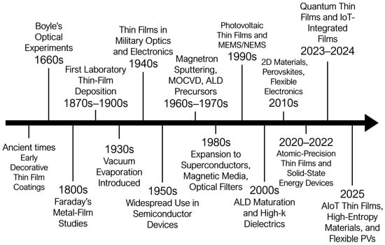
Figure 1.
Evolution of Thin Films.
3. Growth Fundamentals and Physics
3.1. Nucleation
In thin film growth, nucleation acts as a regulator of morphology because the density, spatial distribution, and early size distribution of nuclei formed during the onset of deposition governs the pathway to island coalescence, grain evolution, surface roughness, and ultimately intended functional properties of the film [3]. In general, the physicochemical state that promotes nucleation can be viewed as a competition between a thermodynamic driving force (chemical potential or supersaturation) that promotes the formation of a new phase and interfacial penalties that resist the formation of a new area and interface, such that formation is thermodynamically preferable only when clusters reach a critical compactness [12]. From an engineering perspective, this balance implies that the controllable process parameters—substrate temperature, vapor or flux rate, background pressure, and surface preparation—map directly to nucleation results, and subsequently map directly to device-relevant film performance metrics such as continuity, texture, and defect densities [13].
The hindrance, often indicated as ΔG*, represents the free-energy hill that a cluster must overcome before it can be a thermodynamically stable nucleus in classical definitions, which is dependent on both the supersaturation and the material specific surface energy and interfacial energy values; thereby, relatively small amounts of changes in deposition chemistry or substrate treatments can dramatically change nucleation rate and island density on relevant timescales for technology [14]. In practical terms, ΔG* appears as a kinetic sensitivity: high supersaturation or fast flux favors many small nuclei and rapid coalescence, while low supersaturation or increased surface mobility yields fewer, larger nuclei and smoother layer formation; this is why process engineers purposefully use ramped temperature or pulsed flux approaches to adjust early stages of microstructure without changing chemistry [3]. The classical, continuum view that produces a single ΔG* must be interpreted in concert with atomistic realities at surfaces, such as separate lattice sites, step edges, and fleeting adsorption states, as these affect local energetics and consequently lead to divergences from the simplest homogeneous predictions in actual deposition systems [15].
In thin film nucleation, the surface energy (γ) of the substrate and the depositing material significantly influences the value of ΔG* and the favored growth mode. Surface energy directly affects the wetting properties of the adatoms or clusters via the contact angle (θ), indicating how the deposited phase engages with the substrate surface [16]. When the substrate’s surface energy is significantly higher than that of the film, adatoms are inclined to disperse, leading to a reduced contact angle and a lower effective ΔG*, which promotes two-dimensional (layer-by-layer) or Frank–van der Merwe growth [17]. In contrast, if the film’s surface energy is greater than that of the substrate, inadequate wetting happens, marked by a significant contact angle and an increased nucleation barrier, favoring the three-dimensional island growth typical of Volmer–Weber morphology [18]. In intermediate scenarios, where partial wetting takes place, nucleation initiates as islands that later merge into continuous layers; this exemplifies the Stranski–Krastanov mode [19]. Consequently, the interaction among γ, θ, and ΔG* forms a physical connection between the thermodynamic driving force and the morphological development of the film. Modifying the substrate surface energy—via treatments, coatings, or interfacial engineering—can be an effective approach to influence nucleation energetics and manage the final growth mode without changing deposition chemistry [20].
The wetting angle, θ, is crucial in heterogeneous nucleation—the primary mechanism during thin film formation on solid substrates. It measures the extent of wetting between the deposited phase and the substrate, determined by the equilibrium of interfacial energies at the three-phase contact line, as outlined by Young’s equation:
where represents the substrate–vapor surface energy, denotes the substrate–film interfacial energy, and indicates the film–vapor surface energy. A reduced wetting angle signifies improved wetting and a lower ΔG* for nucleation, promoting two-dimensional (layer-by-layer) growth [21], whereas a larger wetting angle suggests poor wetting and an elevated ΔG*, resulting in three-dimensional (island) growth [3,22]. The physics of wetting behavior and contact angle provide a unified view of the thermodynamics of interfaces with macroscopic growth modes that are seen experimentally, such that the relative magnitudes of substrate–film, film–film, and substrate–film interfacial energies govern whether a film grows layer-by-layer, as three-dimensional islands, or as an initial wetting layer and then islands (Frank–van der Merwe, Volmer–Weber, and Stranski–Krastanov modes) and, if there is lattice mismatch, strain energetics will play a role in the processes [23]. From a materials engineering perspective, the wetting angle is not simply a geometric descriptor but a device to integrate chemical bonding, van der Waals dispersion interactions, elastic relaxation, and the local adsorption environment, and thus a useful design metric for tuning seed layer chemistries or adhesion layers to produce the targeted growth mode [13]. Additionally, intrusiveness or anisotropic surface energies can induce metastable wetting layers of finite thickness before three-dimensional islanding occurs which, in a heteroepitaxy framework, becomes the underlying origin of self-assembled quantum dot formation once elastic relaxation becomes energetically preferable past a critical thickness [24].
Within this framework, the nucleation energy barrier (ΔG*) is primarily determined by the interplay of the interfacial energies that characterize the wetting angle [25]. As ΔG* signifies the energy barrier that needs to be surpassed for a stable nucleus to develop, its value directly indicates the level of wetting: when the substrate’s surface energy is greater compared to the interfacial energy between the substrate and the film, the contact angle reduces, resulting in enhanced adhesion and a decreased ΔG*, which energetically promotes the creation of two-dimensional nuclei that extend over the surface [26]. On the other hand, if the interfacial energy between the substrate and film is high or the film–vapor surface energy prevails, the contact angle rises, signaling inadequate wetting and a higher ΔG*, thus promoting the formation of distinct three-dimensional clusters [27]. Consequently, by mediating the energy balance at interfaces, the wetting angle serves as a macroscopic signal of the microscopic energy dynamics that dictate nucleation. The relationship between γ, θ, and ΔG* offers a thermodynamic basis to explain how slight changes in surface treatments, surfactants, or substrate chemistry can significantly impact nucleation density and growth morphology, even when the deposition conditions remain the same [28].
Curvature-dependent thermodynamics—the Gibbs–Thomson effect—provides additional size dependence on the equilibrium chemical potential and consequently of the stability of nanoscale nuclei, with higher curvature (smaller radius) increasing the effective chemical potential and therefore depressing equilibrium condensation conditions relative to bulk; this provides the thermodynamic basis for phenomena like depressed melting temperatures, suppressed nucleation of very small clusters, and size-dependent solubility in confined geometries [29]. In thin film contexts, the Gibbs–Thomson contribution is fundamental to understanding Ostwald ripening and coarsening dynamics of an ensemble of islands because small islands are thermodynamically favored to dissolve and feed the larger islands unless kinetic barriers inhibit that exchange, thus putting diffusion length and adatom capture efficiencies front and center in scalable film engineering [30]. In terms of device manufacture, this indicates that nanoscale curvature effects manifest as practical constraints on allowable processing windows for features such as quantum dots, nanoparticles in a matrix, or ultrathin continuous films, and exploit surfactants, rapid quenching, or templated nucleation sites to stabilize small nuclei and alter the Gibbs–Thomson effect, promoting dissolution [14]. The Gibbs–Thomson effect presents an extra size-dependent thermodynamic factor by connecting the equilibrium chemical potential of a small particle or cluster to its curvature. This effect states that the equilibrium vapor pressure above a curved surface exceeds that above a flat surface because of the extra energy linked to surface curvature [31]. For a spherical nucleus with a radius r, the Gibbs–Thomson equation can be stated as:
where represents the change in chemical potential compared to the bulk, denotes the surface energy, and signifies the molar volume. In thin film nucleation, this implies that smaller nuclei necessitate greater supersaturation for stability due to their heightened curvature, raising their chemical potential. As a result, the Gibbs–Thomson effect establishes a minimum size for stable nuclei, thereby affecting both the rates of nucleation and the critical thickness required for stable film formation [32].
In general, heterogeneous nucleation on actual substrates will nearly always dominate over homogeneous nucleation, because surface defects, steps, impurities, and specifically designed seeding sites can lower the effective ΔG* by creating lower-energy interfaces or locally changing the wetting geometry. This means that engineers use the density, chemistry, and topography of nucleation sites as a primary way to change nucleation from a stochastic event to a reliable, reproducible step in a manufacturing process [33]. A variety of empirical and theoretical studies show that the density of nucleation sites is a non-linear function of surface energy variations and adatom mobility. This is why combined in situ diagnostics (for example, high-energy electron diffraction (RHEED), in-vacuo AFM/STM, or real-time optical probes) and kinetic models are essential tools in translating laboratory observations into meaningful process windows for production [34]. From an applied viewpoint, practical methods to guide nucleation consist of intentional surface functionalisation to adjust local contact angles, placement of topography-patterned nucleation arrays at the nanoscale to generate deterministic arrays of islands, and brief modulation of flux/temperature, such that desired adatom lifetimes and capture zones ultimately yield the desired nucleus density and uniformity [13].
Linking thermodynamic nucleation ideas with predictive engineering requires simultaneous quantification of kinetics (arrival flux, surface diffusion coefficients, desorption rates) and local energetics (interface energies, strain relief pathways, and chemical interactions with the substrate), since nucleation is a non-equilibrium multiscale process in thin films and only a combined thermo-kinetic description will yield robust process recipes for high-performance films and nanostructures [12]. In practical recommendations for researchers at the review level, we would advise focusing on (i) measuring or estimating interface energies accurately for the film/substrate pair, (ii) experimentally mapping nucleus density against flux and temperature to extract effective ΔG* trends of interest to the researcher, and (iii) systematically investigating wetting-modifying treatments, such as ultrathin adhesion layers or molecular surfactants, moving the growth mode in a desired way, while keeping the limitations of Gibbs–Thomson curvature for nanoscale stability in mind.
3.2. Growth Modes
Thin film growth modes represent a compact taxonomy that connects interfacial thermodynamics and surface kinetics with the macroscopic morphology that develops during the deposition process. Understanding them is important as they set the initial route for grain structure, roughness evolution, and defect incorporation within functional films [3]. The traditional categorization of growth as either Volmer–Weber (island), Frank–van der Merwe (layer-by-layer), Stranski–Krastanov (layers + islands), and step flow growth is more than historical names; they capture the balance of energies between film–film, film–substrate, and the substrate surface energies with strain and kinetic limits [35]. When it comes to applied practice, this taxonomy takes on a practical design ability in that changing substrate chemistry, temperature, flux, or surfactant additions could shift a system from one regime to another and thereby tune electronic, optical, or mechanical performance without changing bulk composition [36]. The morphological evolution of epitaxial thin films is fundamentally determined by the balance between the surface and interfacial free energies of the film–substrate system. Depending on these competing energetics, adatom–substrate and adatom–adatom interactions lead to distinct growth regimes that dictate whether the film develops in two dimensions or transitions into three-dimensional island structures. As illustrated in Figure 2, epitaxial growth can proceed through the Frank–van der Merwe (FM), Stranski–Krastanov (SK), or Volmer–Weber (VW) modes.
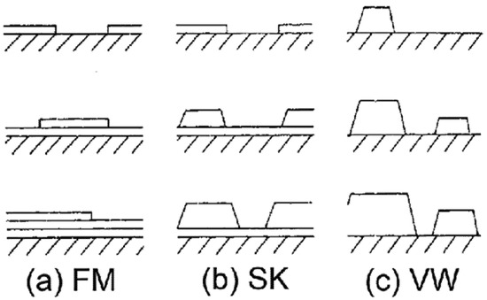
Figure 2.
Schematic representation of the three principal epitaxial thin film growth modes as a function of monolayer (ML) surface coverage (θ): (a) Frank–van der Merwe (FM) layer-by-layer growth, (b) Stranski–Krastanov (SK) layer-plus-island growth, and (c) Volmer–Weber (VW) island growth. The diagrams illustrate how the balance between adatom–substrate and adatom–adatom interactions governs the transition from two-dimensional layer formation to three-dimensional islanding. FM growth occurs when the film wets the substrate completely (γ_substrate > γ_film + γ_interface); VW growth arises when adatom cohesion dominates (γ_substrate < γ_film + γ_interface); and SK growth represents an intermediate regime where strain energy accumulation beyond a critical thickness drives island formation [3,37].
In FM growth, the interfacial bonding between the film and the substrate is energetically favorable, resulting in complete wetting and sequential monolayer formation. This mode minimizes surface free energy and yields atomically smooth films, often observed in systems with minimal lattice mismatch. In contrast, the VW mode emerges when cohesive forces between adatoms outweigh their adhesion to the substrate, producing isolated three-dimensional nuclei from the onset of deposition. Such island growth reflects a condition where the substrate surface energy (γ_substrate) is smaller than the sum of the film and interface energies (γ_film + γ_interface), favoring the clustering of adatoms into discrete islands.
The SK growth mode represents an intermediate mechanism, initiating as layer-by-layer deposition but transitioning to island formation once the strain energy—accumulated due to lattice mismatch—surpasses a critical threshold. This strain-driven instability causes the film to relax via the nucleation of three-dimensional islands atop a wetting layer, thus bridging the FM and VW regimes. The framework depicted in Figure 2, therefore, encapsulates the energetic and strain-mediated principles governing epitaxial growth and serves as a foundational reference for interpreting morphological transitions in strained film systems.
3.2.1. Volmer–Weber Growth Mode
Initially, the Volmer–Weber growth mechanism is distinguished by the formation and evolution of three-dimensional islands, as adatom–adatom interactions dominate over adatom–substrate interactions to produce discrete islands, whose density and size distribution depend strongly on the level of supersaturation and surface diffusion lengths [38]. At the microscopic level, this mode causes high initial roughness, island coalescence that occurs in isolation, and a complex evolution of stresses during coarsening. This has been observed for metals on insulating substrates and for weakly wetting adsorbates [39]. From a kinetic engineering approach, we can modulate Volmer–Weber films by varying flux and substrate mobility such that island nucleation density can be controlled—high flux and low surface mobility produce many small islands, and higher mobility and lower flux lead to large, widely spaced islands and different coalescence pathways [38]. Consequently, the wetting angle is significant, and the thermodynamic impetus encourages aggregation over spreading. The balance of interfacial energy can be expressed as:
where represents the substrate–vapor energy, denotes the substrate–film energy, and indicates the film–vapor surface energy. The inequality signifies partial wetting, resulting in three-dimensional nuclei. This growth mode frequently occurs in systems characterized by substantial lattice mismatch or chemical incompatibility, like metal films (Au, Ag, Pt) on oxide substrates. Volmer–Weber growth often leads to uneven surfaces, polycrystalline microstructures, and a high concentration of grain boundaries, which can be beneficial for catalytic uses but harmful to electronic or optical applications that require smooth films [23].
3.2.2. Frank–van der Merwe Growth Mode
Layer-by-layer growth, known as Frank–van-der-Merwe (FM) growth, yields atomically flat and continuous layers when the substrate–adatom binding is greater than the adatom–adatom binding, and this growth is the thermodynamic ideal for having sharp interfaces and low roughness in heterostructures and devices [40]. The physical signature of this mode is the completion of each monolayer before the next one starts, which requires sufficient adatom mobility to find low-energy sites and a wetting function that is positive, or, to the detriment of the film formation, the creation of new substrate–film interface is energetically encouraged compared to the creation of interfaces between films [35]. Practically, persistent Frank–van der Merwe (FM) growth is exploited in oxide superlattices, semiconductor heterostructures, and other systems where abrupt interfaces and two-dimensional confinement are necessary for the intended functionality [40]. This happens when the interaction between the adatom and the substrate is more intense than the adatom–adatom interaction, fulfilling the requirement:
In this case, the surface free energy of the uncoated substrate decreases during film formation, rendering layer completion energetically advantageous before the nucleation of the subsequent layer. This type of growth occurs in systems characterized by minimal lattice mismatch, high chemical affinity, and matching crystal structures, such as the epitaxial growth of semiconductor films like GaAs on GaAs or Si on Si [41]. The FM mode generates atomically smooth surfaces featuring well-organized crystalline structures, rendering it perfect for high-precision uses in microelectronics, optoelectronics, and quantum devices. Nevertheless, it demands precise regulation of deposition conditions and is extremely responsive to substrate cleanliness and temperature [42].
3.2.3. Stranski–Krastanov Growth Mode
Stranski–Krastanov (SK) growth occupies the intermediate, strain-sensitive niche in which an initial wetting layer forms and then, beyond a critical thickness or chemical potential, three-dimensional islands nucleate to relax accumulated elastic energy, producing self-assembled nanostructures such as quantum dots in heteroepitaxy [43]. The SK transition is controlled by the interplay of interface energies, lattice misfit strain, and kinetics: misfit strain raises the energetic cost of further coherent layer growth so that islanding becomes favorable once the incremental strain energy per added layer eclipses the cost of forming island sidewalls and new interfaces [23]. From an engineering standpoint, this mode is especially powerful because the critical thickness, island size distribution, and spatial ordering can be tuned by deposition rate, substrate vicinality, and intermixing, enabling deterministic approaches to quantum-confined device elements when process windows are carefully mapped [43].
3.2.4. Step Flow Growth Mode
Step flow growth is a kinetically driven, morphology-preserving mode that occurs on stepped or vicinal substrates when adatoms incorporate preferentially at step edges, causing steps to propagate across terraces rather than nucleating new islands on terraces, and this yields macroscopically smooth surfaces even at non-zero growth rates [44,45]. To ensure the viability of step flow growth, it is required that the terrace width and adatom diffusion length be commensurate so that adatoms reach step edges before nucleating stable clusters on terraces, and this makes substrate miscut, temperature, and surface diffusion central knobs for achieving persistent step propagation [45]. In strained systems, step flow growth can persist or break down depending on strain-driven step meandering and step bunching instabilities, and controlling these instabilities through miscut selection and flux modulation is a common route for producing defect-sparse epitaxial films.
Transitions between these modes are neither abrupt nor determined solely by equilibrium wetting criteria; rather, they reflect a competition between thermodynamic driving forces (surface and strain energies) and kinetic constraints (adspecies diffusion, desorption, and supply rate), such that the same material pair can show different modes under different growth conditions [3]. As a result, predictive process design requires measuring or estimating effective surface and interface energies, mapping nucleation density and island statistics as functions of flux and temperature, and incorporating strain relaxation models that account for intermixing and finite temperature effects in realistic deposition regimes. Therefore, modern experimental workflows pair in situ surface probes such as RHEED, in-vacuo AFM/STM, and real-time X-ray scattering with kinetic modeling (rate-equation or kinetic Monte Carlo) to extract mechanistic parameters and translate laboratory observations into robust production recipes [38].
From an engineering perspective, controlling growth mode to target a film morphology is accomplished by three practical levers: tune the effective wetting through interfacial engineering (adhesion layers, surfactants, or surface functionalisation), control adatom kinetics via substrate temperature and flux pulsing or shutters, and utilize substrate templating (vicinal miscut or lithographic nucleation seeds) to bias nucleation to desired locations and scales [35]. Each of these levers carries trade-offs—surfactants can modify electronic properties, high mobility can increase interdiffusion, and templating may complicate large-area uniformity—so optimization requires quantitative feedback from both surface diagnostics and device-level tests in the target application environment [38]. The practical upshot for reviewers and process engineers is that documenting the growth mode, presenting nucleation/island statistics as a function of the principal control parameters, and correlating morphology with the targeted property (electrical mobility, optical linewidth, mechanical integrity) yields a reproducible engineering narrative that bridges fundamental physics and applied fabrication [46,47].
3.3. Adatom Kinetics
Adatom kinetics are the living engine of thin film morphology because the fate of each deposited atom—whether it migrates, attaches to an island, is captured by a step, or desorbs—determines nucleation statistics, island growth pathways, and ultimately film continuity and defect content [48]. Surface diffusion is therefore not a single mechanistic label but a family of atomistic processes that include simple hopping between adjacent adsorption sites, concerted exchange with substrate atoms, long correlated jumps, and periphery motions along island edges, where the dominant mechanism depends sensitively on the material pair, surface crystallography, and local adsorbate interactions [49]. From an engineering perspective, recognizing which mechanism is active in a system is essential because different mechanisms produce distinct effective mobilities, temperature dependences, and responses to surfactants or substrate modification [48].
3.3.1. Surface Diffusion Fundamentals
The diffusion length is the practical, experiment-usable summary variable that captures how far a mobile adatom will travel on average before being immobilized by incorporation or loss, and is the single most useful kinetic metric for linking process conditions (flux, temperature) to mesoscale outcomes such as island density and capture-zone statistics [12]. In real deposition systems, diffusion length is a dynamic quantity determined by the competition between surface mobility and the arrival (or supply) rate of new atoms, and thus is the parameter that determines whether growth proceeds in a regime dominated by heterogeneous nucleation on defects, homogeneous island nucleation across terraces, or step flow incorporation at edges [50]. Practically, mapping the diffusion length experimentally—for example, through island density versus flux/temperature series or by analyzing capture-zone distributions—gives a direct route to extract effective kinetic barriers and to design process windows required for target morphologies in device fabrication [51].
Surface diffusion mechanisms themselves can be subtle: “hopping” across the saddle point of the surface potential energy landscape is common on many metal terraces, whereas an “exchange” mechanism (in which the adatom swaps with a substrate atom) can dominate where the exchange pathway lowers the barrier, and concerted multi-atom moves or long correlated jumps are observed in both experiments and atomistic simulations for a range of material [52]. These mechanistic distinctions matter because they change not only the activation energies that control temperature sensitivity, but also the pre-factors and the effective step-capture probabilities that define how adatoms explore terraces and reach nucleation or incorporation sites [53]. For engineers, this means that a change as simple as switching substrate orientation, adding a sub-monolayer surfactant, or alloying the surface layer can switch the dominant microscopic pathway and dramatically modify the diffusion length and resulting film morphology at the same nominal temperature and flux [48]. The diffusivity of adatoms, , is typically expressed through an Arrhenius-type equation:
where denotes the pre-exponential factor associated with the attempt frequency and jump distance, represents the activation energy for surface diffusion, stands for the Boltzmann constant, and indicates the absolute temperature. A low activation energy or a high substrate temperature boosts adatom mobility by raising the chances of surpassing diffusion barriers among adsorption sites. The microscopic jump rate of an adatom usually ranges from 1012 to 1013 Hz (jumps per second), with the jump distance generally being one surface lattice spacing [54].
The energy required for diffusion is greatly influenced by the characteristics of the surface, such as crystallographic alignment, surface imperfections, and the existence of adsorbates. Diffusion barriers tend to be lower on closely packed surfaces (e.g., fcc(111)) than on more open surfaces (e.g., fcc(100)), and surface steps or kinks may function as traps or barriers based on their arrangement. Moreover, the binding energy between adatoms and substrate atoms can differ greatly among various material systems, affecting the thermodynamics and kinetics of diffusion.
3.3.2. Adatom Mobility and Film Morphology
The movement of adatoms is essential for managing film structure during deposition. Increased mobility enables adatoms to traverse wider regions of the substrate surface prior to being trapped by a developing island or step edge, resulting in the creation of larger grains, smoother surfaces, and more consistent coverage [55]. On the other hand, reduced mobility—resulting from low temperatures or significant diffusion barriers—leads to increased nucleation densities, smaller grains, and rougher films. In epitaxial growth, adequate mobility of adatoms is essential for atoms to locate energetically preferable lattice sites, which guarantees high crystalline quality. Nonetheless, high mobility can lead to undesirable effects like desorption or step flow instability, particularly under high-vacuum or elevated temperature circumstances [56].
Besides thermal activation, external elements like electric fields, ion bombardment, or surfactant layers may affect adatom mobility. For instance, ion-assisted deposition can increase surface mobility locally by delivering extra energy via momentum transfer, whereas surfactants can alter surface energy landscapes, reducing the effective diffusion barrier without being integrated into the film. This idea is utilized in methods like surfactant-assisted epitaxy.
3.3.3. Diffusion Length and Nucleation Dynamics
A crucial factor connecting adatom movements to thin film development is the surface diffusion length, , defined as:
where represents the mean residence duration of an adatom prior to its integration into a stable location. Increased diffusion lengths lead to greater nucleation separation distances, producing fewer but larger islands that merge seamlessly. Short diffusion distances result in densely packed nuclei, resulting in quick coalescence but heightened surface roughness. Control of is essential for adjusting grain size, surface texture, and defect concentration in thin films.
3.3.4. Ehrlich–Schwoebel Barriers and Step-Edge Kinetics
The Ehrlich–Schwoebel (ES) barrier is the canonical kinetic asymmetry that arises when an adatom encounters a step edge and finds an extra energetic penalty for descending (or sometimes ascending) the step, and this step-edge barrier biases mass transport and creates instabilities that control mound formation, step meandering, and the breakdown of layerwise growth [57]. In practice, a positive ES barrier reduces interlayer mass transfer and promotes vertical growth (mounding and 3D islands), whereas a negligible or negative ES barrier allows adatoms to cross steps readily and supports layer-by-layer or step flow morphologies, and the magnitude and even sign of the ES effect have been shown experimentally to vary with material, step facet and the presence of adsorbates or impurities [58]. Contemporary studies have also shown that the ES effect is not strictly a two-dimensional construct and that three-dimensional step geometries, kink sites, and facet-dependent energetics can give rise to a spectrum of effective ES barriers that must be accounted for when predicting texture selection or nanostructure evolution [59].
Because the ES barrier couples directly to step dynamics, it is the primary kinetic origin of many mesoscale instabilities observed during epitaxy, including step bunching, step meandering, and the transition from step flow to islanding on vicinal surfaces, and these instabilities are highly sensitive to the interplay between terrace diffusion length, step spacing (vicinality) and the effective interlayer barrier [59]. Consequently, device-oriented engineers exploit substrate miscut, temperature ramps, and transient flux protocols to tune the ratio between diffusion length and terrace width so as to promote step propagation rather than nucleation on terraces, thereby achieving smoother films with fewer coalescence defects [60]. Moreover, recent atomistic and in situ microscopy work shows that ES barriers on oxide and molecular surfaces can be large and chemically complex, which explains frequent surprises when applying metal-surface intuitions to organic or oxide epitaxy and underlines the need for system-specific measurement or computation of the step-edge energetics [61].
Experimentally, adatom mobilities and ES barriers are extracted using complementary approaches that include direct in situ imaging (field-ion microscopy, STM/AFM), time-resolved diffraction or scattering probes that monitor island density and coarsening in real time, and carefully designed temperature/flux series that allow fitting to rate equation or kinetic Monte Carlo models to yield effective activation energies and diffusion lengths [57]. Low-energy electron microscopy (LEEM) and grazing-incidence small-angle X-ray scattering (GISAXS) have become particularly powerful for following interlayer transport and quantifying ES contributions under realistic growth rates, while STM remains the gold standard for atomistic identification of diffusion pathways and direct observation of processes such as island decay and edge diffusion [62]. For rigorous engineering studies, it is therefore best practice to combine at least one real-space microscopy method with a statistical analysis of island size/distribution evolution such that the measured diffusion lengths and effective ES barriers are grounded in both mechanistic insight and mesoscale statistics [12].
On the modeling side, a hierarchy of tools connects atomistic energetics to macroscopic morphology: density functional or embedded-atom calculations provide the elementary barrier heights and exchange pathways; kinetic Monte Carlo captures stochastic adatom motion and emergent island statistics over experimentally relevant timescales; and continuum or rate-equation descriptions map these kinetics to average fields such as adatom density and surface height for process optimization [48]. Modern workflows increasingly integrate machine-learned surrogate models for migration barriers into kMC frameworks so that high-throughput exploration of substrate treatments, surfactant chemistries, and flux protocols becomes tractable for device-scale engineering [63]. Crucially, predictive simulations must include realistic step geometries and kink diffusion channels to capture ES-driven instabilities and facet selection; otherwise, models risk underestimating defect formation pathways that appear during scaled production runs [51].
In conclusion, surface diffusion and adatom mobility are essential kinetic factors that connect atomic-level processes with the properties of macroscopic films. Adjusting deposition temperature, deposition rate, and surface preparation allows for the engineering of adatom kinetics to promote certain growth modes, enhance microstructural quality, and satisfy application-specific performance needs in electronics, optics, catalysis, and protective coatings. Dominating these kinetic principles is crucial for converting the thermodynamic potential for superior film growth into effective, consistent results in thin film technology.
3.4. Strain and Lattice Mismatch
3.4.1. Strain States and Critical Thickness
The distinction between coherent (fully strained) and relaxed (partially or fully strain-relieved) films is therefore practical as well as conceptual, because coherent layers preserve epitaxial registry and low defect density up to a material-dependent thickness, while relaxed layers frequently exhibit dislocation networks and residual strain inhomogeneity that strongly degrade transport and optical performance in many devices [64]. For this reason, the concept of critical thickness—defined as the nominal film thickness at which misfit-relieving dislocations become energetically favorable—is central to epitaxial engineering. It serves as a primary design parameter that governs strain relaxation behavior and provides a benchmark around which growth processes, buffer-layer architectures, and interface engineering strategies are developed to achieve lattice coherence and minimize defect formation [65,66,67]. It is important to emphasize, however, that critical thickness is not a fixed or universal constant for a given material pair; rather, it depends on parameters such as temperature, growth kinetics, substrate orientation, pre-existing defect density, and the available strain-relaxation pathways [68,69]. Variations in deposition rate, adatom mobility, and interfacial energy can further modify this threshold by altering strain accumulation and dislocation nucleation dynamics. Consequently, practical film design integrates theoretical critical-thickness models with experimental thickness-series measurements, defect mapping, and reciprocal-space analyses to accurately capture the onset of strain relaxation and interfacial instability [70,71]. During the initial phases of heteroepitaxial growth, the deposited film may maintain coherent strain to align with the substrate’s lattice, creating a pseudomorphic layer. This coherent state is energetically advantageous only up to a specific thickness, after which the strain energy in the film becomes significant enough to cause relaxation. The critical thickness () is defined as the maximum thickness for preserving coherent strain without the creation of defects. The historical Matthews–Blakeslee energetic balance gives the earliest and still widely used criterion for when interfacial misfit dislocations become favorable, and that framework links the resolved line tension of a threading dislocation, the lattice misfit, and the geometry of the interface to a threshold for dislocation glide and pinning. Subsequent refinements, such as the People–Bean adaptation, introduced kinetics and more realistic energetic accounting for semiconductor strained layers, producing predictions that align much better with measured critical thicknesses in systems like Ge/Si and SiGe/Si used in microelectronics [64]. Because these continuum models are equilibrium or quasi-equilibrium formulations, modern atomistic and mesoscale studies have shown that kinetic limitations, defect nucleation barriers, and metastable trapping can allow films to remain pseudomorphic far beyond the thermodynamic critical thickness or, conversely, to relax earlier than simple models predict when heterogeneous nucleation sites or elevated temperatures are present [70]. The Matthews–Blakeslee model offers an approximate formula for critical thickness related to mismatch strain and dislocation energy [72].
where represents the Burgers vector of the misfit dislocation, denotes Poisson’s ratio, and indicates the mismatch. This relationship emphasizes that greater mismatches significantly decrease , complicating the growth of defect-free thick films.
3.4.2. Strain Relaxation Mechanisms
Misfit dislocations—the primary plastic carriers of strain relief at interfaces—exist in characteristic geometries (for example, 60° mixed dislocations and 90° edge dislocations in cubic systems) and their nucleation, glide, dissociation, and interaction pathways determine both the rate and the spatial pattern of relaxation [73]. Experimental TEM and in-plane diffraction studies have established that initial relaxation often proceeds via the formation of half-loops or surface-initiated 60° segments that can react or convert into sessile 90° misfit dislocations as the film thickens, a process that creates a complex interfacial dislocation network rather than a single uniform relaxation event. Atomistic modeling and minimum-energy path searches have further revealed multi-step transition pathways for misfit dislocation nucleation—for instance, nucleation of a 60° segment followed by a second complementary event that produces an extended 90° segment—which explains why nucleation energies and observed mechanisms can be very sensitive to surface steps, impurities, and local chemical bonding [74].
Threading dislocations, which penetrate the film from the interface into the overlayer, are the mobile carriers that link interfacial misfit reactions to bulk-like defect populations, and their density, glide mobility, and interactions (including reactions that form Lomer locks or sessile junctions) are the microstructural quantities most closely correlated with device degradation [75]. Consequently, graded buffer layers, low-temperature nucleation layers, compliant substrates, and patterned (selective-area) epitaxy have been developed as engineering countermeasures to reduce threading dislocation density and spatially control where misfit is accommodated. These strategies trade processing complexity for dramatically lower defect densities in many practical material systems [76]. Ion-implantation and post-growth anneals, which influence vacancy/interstitial chemistry and provide routes for dislocation climb and annihilation, are further tools used to accelerate or re-distribute relaxation when precise removal of elastic energy is required for device performance [77].
From a measurement standpoint, the onset and degree of relaxation are routinely quantified by a complementary suite of probes: high-resolution X-ray diffraction provides in-plane and out-of-plane lattice parameters and residual strain, TEM visualizes the dislocation network and core structures at the interface, and high-resolution reciprocal space mapping or grazing-incidence scattering can map partial relaxation and mosaic spread across macroscopic areas [73]. In situ techniques such as real-time RHEED, low-energy electron diffraction (LEED), in-vacuo AFM/STM, and synchrotron grazing-incidence X-ray scattering give access to the dynamic evolution of strain and defect nucleation during growth, which is essential for linking process transients (for example, temperature ramps or flux changes) to relaxation pathways that static post-mortem methods cannot resolve [34]. Quantitative evaluation of threading dislocation densities and interfacial misfit spacing from these probes is the only reliable way to relate a theoretical or modeled critical thickness to practical device yield metrics such as carrier mobility, optical linewidths, and mechanical reliability.
3.5. Stress and Failure
Stress and failure in thin films are central reliability challenges because residual stresses—whether tensile or compressive—alter mechanical stiffness, drive morphological instabilities and, when large enough, nucleate cracking or interfacial delamination that can destroy device function [4]. Residual stresses in deposited films arise from multiple origins and can vary widely with process, material, and post-processing, so effective engineering requires treating stress as an inseparable processing outcome rather than an independent material constant [71].
3.5.1. Sources of Stress in Thin Films
Stress in thin films can generally be divided into three types: intrinsic stress, thermal stress, and extrinsic stress.
- Intrinsic stresses originate during film growth from microstructural evolution, atomic incorporation events, and grain coalescence, and these growth-related stresses can be tensile or compressive depending on the deposition mechanism and energy flux to the growing surface [78]. For polycrystalline and columnar films, tensile stresses frequently develop during the coalescence of islands as boundaries “zip” together and trap misfit strains, while compressive stresses commonly accompany high-energy ion incorporation, peening, and atomic insertion into interstitial sites [79]. Atomistic and structural studies of amorphous and hydrogenated films have further clarified how void elimination, bond reconfiguration, and trapped impurities set the sign and magnitude of intrinsic stress in many technologically important layers [80].
- Thermal stress arises from differential thermal contraction between film and substrate after high-temperature growth or during thermal cycling, and this extrinsic component often dominates in heterostructures processed at elevated temperatures or used in variable-temperature environments [81]. The magnitude of the thermal mismatch stress is a function of the coefficient of thermal expansion difference, the film/substrate elastic moduli, and the temperature excursion, which means even modest CTE mismatch can generate stresses large enough to buckle or crack ultrathin brittle films during cooldown [82]. Thermally induced stresses can also drive time-dependent relaxation via creep or dislocation motion at elevated temperatures, so reported stresses at room temperature may represent a frozen, partially relaxed state that depends on the entire thermal history of the sample [71].
- Extrinsic stresses beyond thermal effects—including chemical reactions with ambient species, moisture uptake in organic films, hydrogen embrittlement, and radiation damage—modify both the mechanical state and interfacial toughness of films and can therefore convert a stable film stack into a progressively failing system under service conditions [83]. Environmental species can induce large compressive or tensile changes by causing swelling, phase change, or volumetric expansion, and such chemically driven extrinsic stress transients are often the trigger for buckling-delamination in multilayers and coatings exposed to humidity or reactive atmospheres [84]. Because extrinsic effects are frequently spatially non-uniform (for example, edge ingress of moisture or local corrosion), they also create stress gradients that favor crack nucleation at specific weak points rather than uniform fracture across the surface [71,85].
3.5.2. Strategies to Minimize Stress and Failure
Predicting failure requires quantifying both the driving force (residual strain energy) and resistances (film fracture toughness and interfacial adhesion), as well as recognizing that these quantities are process-dependent and often history-dependent through plasticity, diffusion, and chemical evolution [86]. Contemporary approaches combine wafer curvature tracking, in situ stress monitoring, microscale blister tests, four-point bend delamination tests, and high-resolution imaging (TEM, SEM, AFM, optical interferometry) to provide the multi-modal data required to parameterise coupled fracture–buckling models [71,87]. Finite-element and analytic fracture mechanics frameworks that incorporate mode-mixity at the interface, substrate compliance, and non-linear film behavior have matured to the point that they can reproduce key experimental observables such as buckle curvature, critical crack spacing, and delamination growth rates when supplied with realistic material and interfacial properties.
From an engineering standpoint, practical mitigation strategies fall into three complementary families: (i) process tuning to manage intrinsic stress—for example, by lowering ion energy, adjusting deposition temperature, or using pulsed flux to change microstructure; (ii) interfacial engineering to raise adhesion and interfacial toughness through adhesion layers, graded interfaces or chemical functionalization; and (iii) structural design such as patterning, compliant buffer layers or controlled thickness grading to limit stored elastic energy per debonded area [78]. Each mitigation pathway carries trade-offs—adhesion layers can change electrical or optical properties, compliant buffers can impact thermal conduction, and patterning can complicate large-area uniformity—so optimization must be driven by the target device metrics and validated by both mechanical testing and functional measurement [88]. Emerging approaches that intentionally harness controlled buckling or programmed fracture for stretchable electronics or micro-patterning show that failure modes can be repurposed as fabrication tools when the mechanics are made deterministic [89].
In conclusion, stress is an inescapable yet controllable part of thin film systems. A comprehensive grasp of stress sources, crack formation processes, and delamination mechanisms enables the creation of improved deposition techniques and structural designs. This guarantees the enduring dependability of thin films in challenging applications like semiconductor devices, optical coatings, protective barriers, and MEMS components.
3.6. Importance and Influence of Substrates in Thin Film Growth and Growth Modes
The substrate acts as the essential base upon which thin films are applied, significantly influencing the growth characteristics, microstructural development, and ultimate functional attributes of the film [90]. From the initial phases of nucleation to surface kinetics, strain accommodation, and stress formation, the substrate continually serves as a governing element that determines thermodynamic equilibrium, kinetic behavior, and mechanical integrity in thin film systems [90,91]. Its impact is multifaceted, covering interfacial energetics, lattice compatibility, diffusion dynamics, and adhesion strength, rendering it essential for producing high-quality and dependable thin films [92].
3.6.1. Thermodynamic Influence and Nucleation Control
The energies present at the surface and interfaces of the substrate are essential in the nucleation process [93]. These influence the wetting properties of the arriving atoms and decide if the film develops as uniform layers or distinct islands. The equilibrium of the substrate–vapor, substrate–film, and film–vapor surface energies determines the contact or wetting angle, serving as a definitive signal of adhesion [94]. A minimal wetting angle indicates effective adhesion and robust adatom-substrate interactions, facilitating smooth, two-dimensional layer-by-layer development. In contrast, inadequate wetting and elevated interfacial energy promote the formation of three-dimensional islands, resulting in rougher surfaces characteristic of Volmer–Weber growth [95].
In intermediate scenarios, the interaction between partial wetting and strain energy buildup results in the hybrid Stranski–Krastanov growth mode, characterized by the formation of several monolayers prior to the onset of islanding [23]. The thermodynamics of the substrate-film interface influences the nucleation process, film coherence, and surface structure [96].
In addition, substrate imperfections like steps, dislocations, and impurities serve as sites for heterogeneous nucleation, lowering the energy barrier for nucleus formation and allowing for localized management of nucleation density [97]. Engineers frequently utilize this principle via intentional surface treatment, like plasma cleaning, chemical etching, or oxide elimination, to establish consistent nucleation patterns and uniform film microstructures [98].
3.6.2. Substrate Structure and Kinetic Regulation
Aside from thermodynamics, the substrate significantly influences kinetic control during thin film development. The adatom mobility, diffusion routes, and incorporation locations are governed by its surface topology, crystal alignment, and atomic structure [99]. Vicinal or stepped surfaces encourage step flow growth, where adatoms move towards step edges and incorporate seamlessly, resulting in atomically smooth films. The diffusion characteristics of adatoms, particularly their capacity to navigate step-edge barriers, are closely related to the potential and geometry of the substrate surface [100].
The substrate also influences how energy inputs like temperature or flux impact growth morphology. Elevated substrate temperatures increase adatom mobility and lead to smoother, equilibrium-like films, whereas reduced temperatures limit movement, causing a high nucleation density and uneven surfaces. Thus, the thermal conductivity of the substrate, surface reconstruction, and orientation together influence adatom dynamics and the shift between various growth regimes [101]. Appropriate choice and preparation of substrates enable the controlled alteration of film morphology without altering deposition chemistry [13].
3.6.3. Lattice Mismatch, Strain, and Interface Coherency
The degree of strain during growth is determined by the structural compatibility between the film and substrate. When the lattice constants are well-aligned, epitaxial films can grow cohesively with few defects, allowing for atomically sharp interfaces and enhanced crystalline quality. This coherence promotes steady, two-dimensional development and is crucial for semiconductor heterostructures and quantum devices [102].
Nevertheless, lattice mismatch generates strain energy that builds up as the film thickness increases. When this strain surpasses a certain threshold, the system adapts via misfit dislocations or the formation of islands, resulting in Stranski–Krastanov or partially relaxed growth [103]. In response to this, buffer layers or graded substrates are frequently employed to facilitate a gradual shift between lattice constants, thereby reducing dislocation density and maintaining crystalline structure [104]. Substrate alignment similarly impacts the distribution of strain at the interface, affecting the chances of defect creation and strain-induced surface reconstruction. Consequently, substrate design serves as an essential engineering mechanism for managing film strain and avoiding degradation caused by defects [105].
3.6.4. Substrate Effects on Stress Evolution and Film Integrity
The mechanical and thermal properties of the substrate greatly influence the residual stress and reliability of thin films. Differential thermal expansion between the film and substrate creates thermal stresses during cooling or thermal cycling, potentially leading to cracking, buckling, or delamination. The substrate’s stiffness and adhesion strength dictate how much stress can be absorbed without causing failure [71,106].
The chemical compatibility at the interface between the substrate and film significantly influences adhesion and durability. Surfaces with appropriate chemical properties, or altered with adhesion-enhancing interlayers like titanium, chromium, or silicon oxide, can greatly improve bond strength and reduce environmental damage [107]. Consequently, substrate engineering influences both the film’s microstructure and its durability against operational stresses over time [108].
3.6.5. Engineering Significance and Practical Implications
In practical thin film engineering, the substrate acts as more than just a passive support; it actively influences growth behavior, structure, and performance. By careful choice and surface modification, substrates facilitate:
- Regulation of growth modes through the adjustment of interfacial energies and wetting characteristics [109].
- Enhancement of film consistency and texture through surface designs or tiered shapes [110].
- Decreasing strain and defect densities via lattice-matched or flexible buffer layers [111].
- Enhanced adhesion and longevity through chemical alterations or graded interfacial designs [112].
In conclusion, the substrate is the primary controlling element in the growth of thin films. It governs the thermodynamic environment for nucleation, the dynamic routes of adatom displacement, and the structural basis for stress development. Expertise in substrate characteristics and preparation enables exact regulation of film morphology, quality, and functionality, thereby connecting theoretical growth models with actual device manufacturing.
4. Thin Film Deposition Techniques
Thin film deposition is integral to the development of contemporary electronic, optical, or nanostructured devices. This process involves applying a controlled thickness of material (a few nanometers to a few micrometers). The role of thin films is to improve surface properties such as conductivity, reflectivity, corrosion resistance, and strength [113].
Technologies for deposition processes are expanding and have led to a variety of deposition techniques to satisfy the requirements for advanced applications. Thin film deposition is often classified as physical, chemical, and electrochemical processes, and there are advantages with each type of technique in terms of quality of the film, adhesion, uniformity, and scalability [114]. Different deposition techniques can produce thin films with various structural and electrical properties based on the type of material deposited and the substrate. The material to be deposited will dictate the choice of deposition technique, along with consideration of the substrate, the operating temperature, and the desired properties [115].
4.1. Physical Vapor Deposition Techniques
Physical Vapor Deposition (PVD) covers a family of vacuum deposition techniques in which a solid material is physically transformed into a vapor state and allowed to condense on a substrate to form thin films [116]. While some techniques involve chemical processes, PVD processes are purely physical processes, such as evaporation, sputtering, or ablation, where material is simply moved to the substrate through transfer [117]. PVD processes are very beneficial for producing coatings that require high purity, high performance, good adhesion, and uniformly thick films for a variety of applications. The technologies are important for areas such as microelectronics, optics, aerospace, and tools in which film thickness and composition require precision control during deposition [118]. The principal PVD techniques typically include thermal and electron beam evaporation, various sputtering techniques, continuous wave and pulsed laser deposition, ion beam deposition, and cathodic arc deposition. Each process can offer specific advantages primarily related to deposition rate, film density (or porosity), and capacity or ability to coat complex parts [118].
In conventional Physical Vapor Deposition (PVD), material from a solid target is ejected through direct current (DC) magnetron sputtering, and the resulting neutral atoms travel through the vacuum to deposit directly onto the substrate surface. The process is governed primarily by physical collisions between the target and plasma ions, with limited control over the ionization state and directionality of the deposited flux. However, in Ionized Physical Vapor Deposition (iPVD), an additional radio-frequency (RF) powered plasma is introduced between the target and substrate, creating an intermediate plasma zone that enhances the ionization of sputtered silicon species before deposition. This increased ionization allows the film-forming species to be accelerated and guided by the sheath electric field toward the substrate, thereby improving step coverage, adhesion, and film density—even at low or room temperatures [119].
The underlying principle is that the additional RF plasma increases the fraction of ionized atoms relative to neutral species, resulting in a more energetic and directed deposition flux. This enables superior microstructural control, particularly on complex or high-aspect-ratio surfaces, compared with the conventional PVD process, where only neutral atoms contribute to film growth. The comparative schematic shown in Figure 3 illustrates these fundamental distinctions, where panel (a) represents the neutral atom-based PVD process and panel (b) depicts the iPVD configuration featuring an RF-induced plasma region that generates ionized silicon flux for enhanced thin film formation.
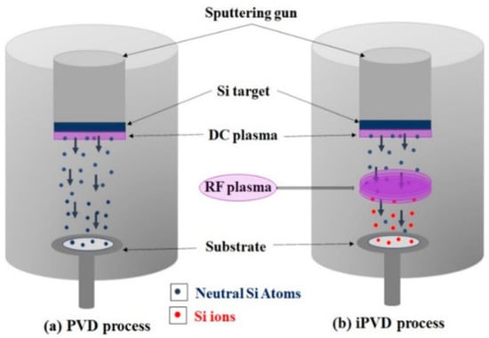
Figure 3.
Schematic representation of (a) conventional Physical Vapor Deposition and (b) Ionized Physical Vapor Deposition processes [119].
4.1.1. Thermal Evaporation Technique
Thermal evaporation is a basic PVD technique and is typically the one that produces the highest-purity thin films. Thermally vaporized source materials are heated in a vacuum, and the vapors are condensed on a substrate. The ‘thermal’ aspect of the technique relies on the use of resistive heating to raise the source material’s temperature to its vaporization point. Typical resistance heating sources include filament wires, boats, or crucibles made from ‘refractory metal’ sources such as tungsten and molybdenum, which are durable and stable under vacuum due to their mostly high melting points. The source material vaporizes and releases atoms or molecules into the vacuum, usually linearly, due to a lack of collisions (low chamber pressure, typically from 10−5 to 10−7 Torr). The vaporized materials reach a relatively cooler substrate above the source and condense to form a continuous film layer [120].
The rate of deposition is often measured in real-time using a QCM and, of course, will be affected by all of the parameters like source temperature, source vapor pressure of the deposited material, distance from the source to the substrate, etc. In addition to producing thin films which are highly pure, dense, and smooth, because there are no reactive gases present and the kinetic energy of individual particles is quite low during thermal evaporation, allows for high-quality thin film deposition [121].
In the Thermal Evaporation Technique, a high-purity solid source material is resistively heated inside a high-vacuum chamber until its vapor pressure becomes sufficient for atomization. The vaporized species then travel through the evacuated environment in a line-of-sight trajectory toward the substrate, where they lose kinetic energy and condense to form a dense, uniform thin film. Because the deposition takes place under low pressures (typically 10−5–10−6 mbar), collisions between vapor atoms and residual gas molecules are minimized, ensuring high-purity film growth with excellent control over thickness, stoichiometry, and surface morphology [122]. The overall working mechanism of this process is depicted in Figure 4, which illustrates the resistive heating of a silicon or metallic source using a tungsten boat, vapor-phase transport through the vacuum chamber, and subsequent condensation and nucleation on the cooled substrate surface. Such controlled physical vapor transport allows the fabrication of films with superior adhesion and uniformity, particularly useful for optoelectronic and dielectric applications.
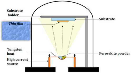
Figure 4.
Schematic diagram of the Thermal Evaporation Technique [122].
Film uniformity and adhesion are influenced by factors such as substrate temperature, surface cleanliness, vacuum quality, and deposition rate [123]. Poor step coverage is a well-known limitation, as the vapor travels in a line-of-sight path that makes it difficult to coat exposed sidewalls or features in recessed areas on a structured substrate. To improve step coverage, vendors now provide rotary stages, hot/cool rotating stages, and planetary holders.
Additionally, because thermal evaporation is a non-reactive method of deposition, a reactive gas must be used to form compounds (e.g., nitride or oxide) during or after the deposition process. Despite these constraints, thermal evaporation is still a requirement in a number of technology areas because it is easy to operate, low cost, scale-up, and can be performed on sensitive substrates.
Thermal evaporation is widely used for semiconductor fabrication, optical multilayers, photovoltaics, surface passivation, sensor work, and vacuum metallization for decorative or barrier purposes. Even in a research setting, thermal evaporation is a well-understood and practical deposition method that has been used to prototype nanostructured films, deposit quantum dots, and functional coatings in state-of-the-art materials research [124]. Its capability to produce highly uniform films, while maintaining nanometer-level film thickness, in various cleanroom-compatible conditions has ensured that thermal evaporation will continue to play a major role in thin film technologies.
4.1.2. Electron Beam Evaporation
Electron beam evaporation is an advanced PVD process. It is a high-precision technique that deposits high-purity, dense, and uniform thin films. This allows for high-purity deposits because it utilizes a focused high-energy electron beam to thermally evaporate source material instead of resistive heating. The source material is generally provided from a heated element, or tungsten filament, that emits electrons. These electrons are then accelerated using a high-voltage electric field, commonly between 5 and 20 kV, before being affected by magnetic or electrostatic fields to direct the focused energy onto the source material [125]. The source material needed for evaporation is then placed in a copper crucible, often cooled with water, which allows for a large area deposit. This crucible usually allows for multiple “pockets” (multi-pocket configuration) to allow for either sequential or composite/combined evaporation. The high-energy electron beam delivers both high-intensity and localized energy to the source material, which means that source materials with even high melting points (tungsten ~3422 °C, molybdenum ~2623 °C) are melted and evaporated without heating or melting the chamber or crucible, and dramatically reduces thermal stress and possible contamination [125].
In the Electron Beam Evaporation (EBE) system, as illustrated in Figure 5, a high-energy electron beam generated by thermionic emission from a tungsten filament is accelerated under a high-voltage electric field and magnetically focused onto the source material positioned within a water-cooled copper crucible. Unlike conventional resistive heating, this method enables localized and precisely controlled energy delivery, allowing the evaporation of materials with extremely high melting points such as tungsten (~3422 °C), molybdenum (~2623 °C), and alumina (~2072 °C). The concentrated beam melts and vaporizes the target surface while minimizing thermal load on the surrounding chamber components. The vaporized species then traverse the vacuum space (typically maintained at 10−5–10−6 Torr) in a line-of-sight trajectory before condensing onto the substrate to form a dense, uniform, and adherent thin film. The electron source, focusing–deflection assembly, and crucible geometry are designed to ensure beam stability and deposition uniformity, enabling the fabrication of high-purity coatings with nanometer-level control over film thickness and composition [126].
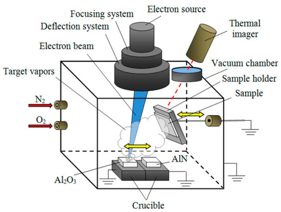
Figure 5.
Electron Beam Evaporation [126].
The complete procedure takes place in a high vacuum environment (typically 10−6 to 10−8 Torr), which ensures that the vapor atoms have a long mean free path and that collisions, oxidation, or contamination are unlikely. The vaporized atoms then condense onto a cooler substrate located vertically to the vapor source as a thin, uniform, and adherent film [126]. Due to the directional nature of the evaporation, it is common practice to rotate or tilt the substrate holders for uniformity and improved step coverage. Various in situ monitoring systems, such as QCM, provide the deposition rate in order to allow real-time control over film thickness and deposition rate, frequently at nano-scale precision [127].
One of the primary strengths of electron beam evaporation is the ability to deposit ultra-high purity films with excellent adhesion and optical clarity. In many ways, it is the process of choice for metals, semiconductors, dielectrics, and even ceramic materials such as Al2O3, TiO2, SiO2, and ZrO2. Furthermore, by carefully adjusting the configuration of the beam and crucible, it is possible to fabricate complex multi-layer structures, alloys, and composite films with very specific and controlled stoichiometries, which is often difficult to achieve with conventional thermal evaporation.
This method has more complex infrastructure than thermal evaporation, such as the high-voltage power supply, the beam-focusing and -deflecting equipment, heavy-duty vacuum equipment, and shielding against radiation. Furthermore, the X-rays that are generated when the high-energy beam hits the target can cause damage to sensitive substrate materials for semiconductor devices.
Despite the complexity of the infrastructure, there are several high-end applications that cannot do without electron beam evaporation as a deposition technique. It is commonly used for the fabrication of semiconductor devices, when incorporating optoelectronic devices, solar cells, dielectric mirror coatings, thin film capacitors, MEMS components, and aerospace-grade optical filters. It is valuable in research laboratories for the fabrication of ultra-thin films and or nanostructures, for research in advanced materials science and surface engineering. Within the thin film technology field, electron beam evaporation remains an important industrial production and experimental research deposition technology because of its guaranteed film quality, good thickness control, and ability to double or multiple source materials.
4.1.3. Sputtering Techniques
Sputtering is a commonly used PVD approach, where atoms are ejected from a solid target material through the bombardment of energetic ions (typically from an argon plasma). The atoms are ejected and travel through vacuum space to a substrate where they condense to form a thin film. Sputtering generally produces excellent adhesion, dense films, and good coverage of complex geometries. Sputtering is especially suited for the deposition of metals, alloys, semiconductors, and insulators for compounds [128]. Several types of sputtering are used to optimize different deposition for different materials and uses, including DC sputtering, RF sputtering, Magnetron sputtering, and Reactive sputtering.
In sputtering-based Physical Vapor Deposition (PVD), as illustrated in Figure 6, a solid target material is bombarded by energetic ions—typically argon plasma ions—generated within a magnetron-assisted vacuum chamber. The momentum transfer during these high-energy collisions causes the ejection of target atoms, which then travel through the plasma environment and condense onto the substrate to form a thin film. This technique enables excellent adhesion, dense microstructures, and uniform coverage even on complex surface geometries. Compared with conventional evaporation-based methods, sputtering offers superior film–substrate bonding strength due to the higher kinetic energy of incoming species and allows for precise control of deposition parameters such as substrate bias, working pressure, and plasma power. Such controllability makes sputtering particularly suitable for depositing refractory metals, dielectric oxides, and compound semiconductor films where stoichiometric accuracy and structural integrity are critical.
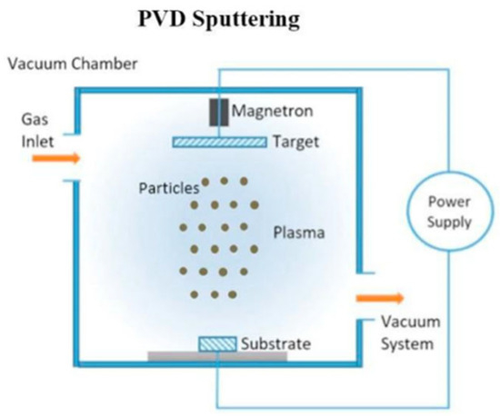
Figure 6.
Schematic representation of the Physical Vapor Deposition (PVD) sputtering process, illustrating ionized argon bombardment of the target within a magnetron-assisted vacuum chamber and the subsequent transport and condensation of ejected atoms on the substrate surface to form a thin film [116,129].
DC Sputtering
DC Sputtering is a fundamental and versatile PVD process that is commonly used for the deposition of electrically conductive thin films from materials of any option of composition (e.g., metals and alloys) [130]. In the process, a negative direct current voltage is applied to the target material, which acts as the cathode, and the substrate is either grounded or held at a slight positive potential. An inert gas (most frequently argon) is introduced into a vacuum chamber that is maintained at relatively low pressures that typically range from 10−3 to 10−6 Torr. The voltage applied to the target ionizes the argon gas, forming a relatively stable plasma of ionized argon (Ar+ ions) and electrons [131]. The Ar+ ions are positively charged and are accelerated towards the negative bias of the target material. The initial kinetic energy of the Ar+ ions is determined by the voltage that is applied to the target material. When the Ar+ ions strike the surface of the target with sufficient energy, the surface atoms of the target will be physically ejected from the surface in a process that is referred to as sputtering. The sputtered atoms can travel through a vacuum rapidly and will condense onto the substrate into a thin film. The morphology of the as-sputtered film will depend on several variables, such as voltage and substrate-to-target distance, but the majority of as-sputtered films will be thin and uniform, and adhere well [132].
DC sputtering has many advantages, such as simplicity and low cost, in addition to its ability to produce dense, well-adhered coatings. DC sputtering provides a perfect way to deposit pure metals, metal alloys, and some conductive compounds, but it cannot be used to deposit insulating materials. Non-conductive sputtering target materials subjected to a constant ion bombardment will accumulate charge, leading to disruption of the plasma and stopping the sputtering process completely. The deposition rates in DC sputtering are moderate, and the deposition rate can be controlled by the power input, the pressure in the chamber, and the distance between the target and substrate. DC sputtering can provide good film uniformity for flat surfaces; for more complex geometries, the substrate usually has to move. DC sputtering is used for metal interconnects in microelectronics, for back contact layers for solar cells, and for optical coatings such as reflective or conductor coatings. Despite some limitations, the robust and reliable characteristics of DC sputtering have made it the foundation of thin film deposition methods for both academic and industrial materials applications [133].
RF Sputtering
RF Sputtering is a type of sputtering deposition that goes beyond DC sputtering. More specifically, it makes use of DC sputtering to effectively deposit insulating (non-conductive) materials like oxides, nitrides, or ceramics. RF sputtering operates by using an Alternating Current (AC) at a standard radio frequency, 13.56 MHz, which is globally allocated for industrial use to avoid electromagnetic interference with communication systems [134]. RF sputtering uses a high-frequency alternating voltage applied to the target material located in a vacuum chamber with an inert gas, typically argon. The main advantage of the alternating field is that it alternately switches the polarity of the target and substrate. This prevents the buildup of positive charge on the insulating targets, which would deactivate ion bombardment in a DC technology. The sputtering process can continue uninterrupted in DC sputtering only with dielectric or insulating materials [135].
In radio-frequency (RF) magnetron co-sputtering, simultaneous operation of multiple RF-driven targets within a controlled Ar/O2 plasma allows the deposition of complex multicomponent oxide thin films with excellent stoichiometric precision. Each target—typically composed of high-purity oxide or carbonate precursors—is connected to an independent RF power supply, enabling individual control of sputtering rates and thus compositional tuning at the atomic scale. The alternating RF field sustains a stable plasma discharge at low pressures (10−3–10−2 mbar) by periodically reversing the electrode polarity, preventing charge accumulation and permitting the sputtering of insulating materials. Magnetron confinement of the plasma near the target surface enhances ionization efficiency, reduces substrate heating, and promotes a high deposition rate. Substrate heating (400–700 °C) further increases adatom mobility, facilitating epitaxial nucleation and dense microstructural growth [136].
As illustrated in Figure 7, the deposition chamber comprises three magnetron cathodes oriented toward a rotating, resistively heated substrate holder with precise gas-flow control for Ar and O2. This geometry minimizes re-sputtering and cross-contamination while ensuring thickness uniformity across the substrate surface.
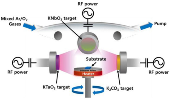
Figure 7.
Schematic diagram of the home-built off-axis RF magnetron co-sputtering system equipped with three independently powered sputtering guns for multi-component oxide film growth. The setup operates under an Ar/O2 gas mixture with controlled substrate heating, enabling stoichiometric tuning and uniform deposition of complex perovskite thin films [136].
In RF (radio frequency) sputtering, the sputtering process relies on an oscillating electric field that produces steady and denser plasma at lower gas pressures compared to DC, improved ionization efficiency of the sputtered target, and better control over the properties of deposited films. During the sputtering process, the electrons in the plasma are faster and therefore more mobile in the field than the ions and respond directly to the rapidly varying RF field [137]. This unique scenario creates a self-bias on the target, which will allow the target to continuously be bombarded by ions. This bombardment allows the target atoms or molecules to be ejected from the target and deposited on the substrate as a thin film with good adhesion and uniformity. While RF sputtering adds versatility, there is a downside: the requirement of more complicated power supplies and impedance matching networks to generate stable plasma conditions, which ultimately adds to the overall cost and complexity of the sputtering system, compared to DC sputtering.
Regardless, RF sputtering is one of the most important techniques used in thin film technology because it is able to deposit good-quality dielectric films like SiO2, Al2O3, TiO2, ZnO, and some compound semiconductors. For use in devices such as semiconductors, optical coatings, thin film capacitors, sensors, and most MEMS devices, dielectric or transparent materials are often found to be desirable [138]. RF sputtering can also produce multilayer structured films and composite films. It has excellent control over film thickness, stoichiometry, and uniformity, and is the only practical technique for depositing thin films on both conductive and non-conductive targets. Therefore, RF sputtering is one of the most versatile and widespread sputtering methods used in both industry and research.
Magnetron Sputtering
Magnetron Sputtering is an effective enhancement of the conventional DC or RF sputtering process and is the most commonly used enhancement process. This technique will improve the deposition rate, quality of the film, and increase the plasma density [139]. In magnetron sputtering, strong permanent magnets are positioned behind the sputtering target (cathode) to create a magnetic field that is perpendicular to the electric field in the sputtering chamber. The magnetic field causes free electrons, which are created during the sputtering process, to be trapped in proximity to the target surface and forced into a spiral trajectory towards the target, thus increasing the chances of collisions between electrons, ionization, and neutral inert Argon atoms. The result is an enhancement in ionization efficiency that produces a dense and stable plasma at lower gas pressures. In magnetron sputtering, there are more positive ions (Ar+) between the plasma surface and the target that can accelerate and bombard the sputtering target surface. The net result is an increase in sputtering from the target [140].
Magnetron sputtering offers a higher deposition rate, better material utilization, and lower heating of the substrate than traditional sputtering, as it concentrates the plasma in the vicinity of the target and therefore energy is not spread out throughout the chamber. In this way, slippery magnetron sputters reduce substrate damage of sensitive substrates and reduce unwanted contamination of the films by exogenous films, at least to some extent. Magnetron sputtering can be used with a DC power supply for conductive targets or with an RF power supply for insulating films, leading to flexibility over the types of materials that could be deposited. It is also hugely scalable and can be used to uniformly deposit a thin film over large-area substrates, providing a number of advantages for industrial manufacturing.
In magnetron sputtering, as illustrated in Figure 8, a magnetic field generated by a set of permanent magnets confines secondary electrons near the target surface, thereby increasing ionization efficiency and maintaining a dense plasma even at low working pressures. The orthogonal arrangement of the magnetic and electric fields creates a closed-loop electron path, enhancing plasma stability, target utilization, and deposition uniformity. During operation, positively charged argon ions (Ar+) are accelerated toward the negatively biased target, transferring momentum that ejects surface atoms. These sputtered atoms then traverse the plasma region and condense onto the substrate, forming a dense, adherent thin film with excellent compositional control. The localized magnetic confinement reduces the thermal load on the substrate while improving film growth rate and homogeneity across the deposition area [141].
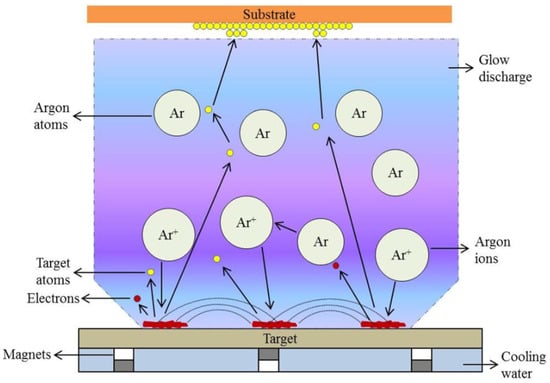
Figure 8.
Schematic representation of the magnetron sputtering system, illustrating the interaction of electric and magnetic fields near the target surface that confines secondary electrons to enhance plasma density and ionization efficiency. The arrangement includes the cathode target embedded with permanent magnets, argon gas inlet, plasma discharge region, and substrate holder positioned to enable uniform thin film deposition [141].
There are many magnetron designs to maximize performance for specific applications. In balanced magnetron sputtering, the magnetic field is closed around the target, keeping plasma extension limited and causing less bombardment of the substrate, making it ideal for thin, positional coatings with precision. While balanced magnetron sputtering, in contrast to unbalanced magnetron sputtering will intentionally leaks the field, allowing the plasma to be directed more toward the substrate and/or the associated atoms to be deposited, which may also promote the best film adhesion and/or ion-assisted growth. There are also dual systems where co-deposition occurs either with sequential or simultaneous operation of the magnetrons; these systems are generally used for reactive sputtering, or for two or more alloys and compounds [142].
Magnetron sputtering is overwhelmingly utilized in various industries because it is fast and flexible relative to its competitors. For example, it is used to deposit metal contacts or diffusion barriers in semiconductor device fabrication, transparent conductive oxides (e.g., indium tin oxide (ITO) or ZnO) in solar cell manufacturing, mirror or anti-reflective coatings in optical coatings, and hard coatings in cutting tools, wear-resistant surfaces, and decorative finishes. Furthermore, it has been accepted as a dominant process in the semiconductor and solar industries in light of its capacity to produce films with excellent density, adhesion, and uniformity, which has made magnetron sputtering the process of choice for collaborative high-volume production or advanced research [143].
Although Physical Vapor Deposition (PVD) methods—such as sputtering and evaporation—are renowned for producing high-purity, versatile thin films, they are constrained by both technical and economic factors. The necessity for ultra-high vacuum environments, meticulous substrate temperature control, and costly target materials elevates operational expenses and maintenance demands [116]. Moreover, being inherently a line-of-sight process, PVD struggles with inadequate step coverage and non-uniform coatings on substrates with intricate geometries. Challenges related to film adhesion, intrinsic stress, and particulate contamination further undermine reliability in multilayer or flexible device fabrication. Limited scalability, coupled with low throughput and large equipment footprints, restricts its suitability for affordable mass production. Consequently, despite its maturity and excellent film quality, PVD requires substantial optimization in uniformity, cost-effectiveness, and environmental sustainability to sustain its competitiveness in next-generation thin film manufacturing [133].
4.2. Chemical Vapor Deposition
Chemical Vapor Deposition (CVD) is a popular method for thin film deposition, which involves the reaction or decomposition of volatile precursor gases on a substrate. The precursor gas interacts or reacts with the heated substrate to form a solid thin film. The CVD process occurs in a controlled environment, usually at a vacuum or reduced pressure, to minimize variations in film formation and promote uniformity. CVD methods produce conformal, high-purity, and high-adherence films and are a key technology in the semiconductor, microelectronics, optics, and coatings sectors. Several CVD variants have been developed to suit different materials systems, substrate sensitivities, and process conditions [144].
The CVD process involves introducing volatile precursor gases into a heated reactor chamber, where controlled thermal energy drives chemical reactions that result in thin film formation on the substrate surface. As depicted in Figure 9, the experimental setup consists of a horizontal quartz tube furnace with distinct inlet and outlet regions for the reactant gases, a central heating zone containing a ceramic crucible loaded with TiO2 precursor, and a substrate positioned to ensure uniform gas–substrate interaction. This configuration enables consistent film growth by maintaining a steady reactant flow and thermal gradient across the reaction zone, thereby enhancing coating homogeneity and adhesion [145].
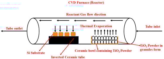
Figure 9.
Schematic representation of the Chemical Vapor Deposition (CVD) furnace system illustrating the reactant gas flow path, substrate position, and precursor arrangement inside the ceramic reaction tube. The setup comprises a horizontal quartz tube reactor equipped with a controlled heating zone, gas inlet and outlet, and a crucible containing the TiO2 precursor powder. This configuration facilitates uniform reactant gas distribution, thermal decomposition, and subsequent film deposition on the Si substrate [145].
4.2.1. Conventional Chemical Vapor Deposition
Thermal CVD, often simply referred to as CVD, is a standard thin film deposition technique that relies solely on thermal energy to initiate chemical reactions or to decompose precursor gases in the form of vapors or gases on a heated surface (the substrate). In a CVD system, precursor gases are introduced to a reaction chamber held at high temperatures (600 °C to 1100 °C). The precursor gases generally chemically react or thermally decompose on the surface of the heated substrate, forming a solid film, while by-product gases are expelled from the chamber vents using a venting system [146]. The heating is generally provided using resistive heaters, induction coils, or radiant heat, and the substrate is controlled at a particular temperature to control the reaction kinetics and deposition rates.
In a CVD system, reactive precursor gases are introduced into a heated reactor chamber where they undergo controlled thermal decomposition and chemical reactions to deposit thin films on the substrate surface. The overall process efficiency is governed by the interplay between gas-phase kinetics, surface reaction rates, and mass transport phenomena [147]. As illustrated in Figure 10, the CVD apparatus typically comprises a gas inlet system, a heated reaction chamber, and a substrate positioned within the uniform temperature zone to ensure homogeneous coating formation. The system operates under a carefully regulated flow of reactive and inert gases, enabling precise control of film thickness, stoichiometry, and microstructure.
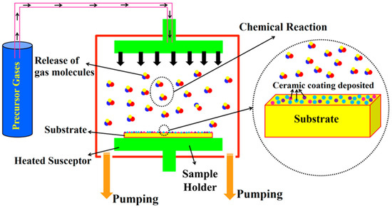
Figure 10.
Schematic representation of a CVD system used for the deposition of ceramic nanocomposite coatings. The setup includes a controlled gas delivery system, a reaction chamber with heating elements, and a substrate positioned in the central hot zone where gaseous precursors react to form solid films. As the reactive gases pass through the heated zone, they undergo decomposition or chemical reaction near the substrate surface, leading to film formation, while inert gases such as argon serve as diluents to maintain uniform pressure and flow [147].
CVD is highly applicable as a deposition procedure and is applicable to a range of materials, particularly for the microelectronics and semiconductor industries, such as silicon (Si), silicon dioxide (SiO2), silicon nitride (Si3N4), tungsten (W), and other metals or dielectric films. One major advantage of this method over others is the high-quality, dense, and conformal films created under a range of values, including high aspect ratios and a variety of substrate shapes. This makes it particularly advantageous for coating 3D structures, trenches, and vias in integrated circuits and MEMS devices [148].
A major limitation of conventional CVD is the high operating temperature, as it narrows the available materials to deposit to those that can additionally withstand high temperatures such as metals, ceramics, and certain glasses. Extended high-temperature exposure can also lead to reaction of the film and substrate, or development of thermal stresses, necessitating careful optimization of the processes. Additionally, there may be undesired gaseous by-products that must be dealt with in ways that minimize their potential for contamination, corrosion, or any other unintended consequence. For example, HCl, NH3, and CO can all be problematic depositions if too many by-products are produced [149].
Notwithstanding the above problems, thermal CVD is hugely scalable and is usable in both batch and continuous depositions, and will soon be developed to enable deposition in a wider variety of materials. Traditional CVD has a relatively straightforward system architecture with a proven recommendation of reliability, making thermal CVD a favorite CVD-deposition method in high-throughput production environments, especially for semiconductor fabrication, photovoltaic cells, optical coatings, and hard protective layers. In addition, the fine control of variables in thermal CVD, such as gas flows, pressures, and temperatures, contributes to engineers making desired adjustments to film properties, including film thickness, grain structure, stoichiometry, and crystallinity. Regardless of the high thermal costs, conventional CVD remains one of the more important techniques within the thin film deposition methodology [149].
4.2.2. Low-Pressure Chemical Vapor Deposition
Low-pressure chemical vapor deposition (LPCVD) is an improved process for vapor phase deposition, as compared to thermal CVD, that provides a process environment at a much lower pressure ranging from 0.1 to 1 Torr. Since the process pressure of LPCVD is significantly lower than CVD, this means that the likelihood of gas-phase collisions and homogeneous reactions in the vapor phase is minimized. Consequently, this lowers the potential for particle formation and (most importantly) improves the conformality and uniformity of the film deposited to the surface of the substrate. The low pressure allows the gas molecules a greater mean free path, which will enable more directed transport of both precursor gases to the substrate and improved step coverage across not just two-dimensional surfaces, but onto complex three-dimensional structures [150]. LPCVD typically utilizes a hot-wall reactor (horizontal or vertical) and radiant or resistive heating. LPCVD also typically takes place at high temperatures from 550 to 900 °C, based on the material system.
LPCVD is most simply used for the deposition of polycrystalline silicon (poly-Si), silicon nitride (Si3N4), and silicon dioxide (SiO2); the materials of choice when creating semiconductor devices or MEMS devices, or for IC passivation or insulating layers. The process is considered to produce films that are dense, high-purity, highly reproducible, and with low defect density. LPCVD is also especially useful for batch processing, more specifically, wafer processing. Moreover, LPCVD can provide good as-coated layer thickness uniformity across each wafer and between multiple wafers if processed at the same time, providing an additional increase in throughput while also lowering the cost per unit in high-volume manufacturing environments [151].
LPCVD still operates at quite high processing temperature, just like conventional thermal CVD, which can limit its applicability to temperature-sensitive substrates or pre-processed layers. Also, while the lower pressure reduces particle contamination, the need for a vacuum apparatus adds some complexity and expense to the whole system. Nonetheless, LPCVD is a foundational technology at the heart of the microelectronics industry because it provides a good compromise amongst film quality, scalability, and regulatory process. There are a variety of applications, including dielectric spacers, diffusion barriers, gate dielectrics, inter-layer insulators, flat-panel displays, and solar cells [152]. LPCVD still has high precision, great step coverage, and high film quality properties. It is still the technology of choice everywhere where thin film deposition is performed to satisfy the advanced processing requirements.
4.2.3. Plasma Vapor Deposition
Plasma-Enhanced Chemical Vapor Deposition (PECVD) is a modified version of CVD that uses a plasma discharge to create a greater chemical reactivity from the precursor gases. This allows for thin films to be deposited at much lower substrate temperatures, generally between 100 °C and 400 °C. This is a significant advantage over thermal CVD processes, which typically operate above 600 °C. Therefore, PECVD has special advantages when using thermally sensitive substrates such as polymers, glasses, or commercial fabrication semiconductor devices [153]. The process is started in a vacuum chamber using either an RF (radio frequency) or microwave power source, which ionizes the process gases, creating the plasma. The energetic electrons in the plasma easily dissociate and activate gas-phase molecules, and allow surface reactions to occur on the substrate to produce the solid film.
Due to its lower thermal budget, PECVD is well-suited for applications that require low-temperature processes, including organic electronics, flexible electronics, and back-end-of-line (BEOL) semiconductor processes. PECVD is a common technique for deposition of several materials, including silicon dioxide (SiO2), silicon nitride (Si3N4), hydrogenated amorphous silicon, and diamond-like carbon (DLC) films. Additionally, one of the prominent advantages of PECVD is the ability to deposit hydrogen-rich films that will passivate defects found in materials such as amorphous silicon, which is an important aspect to achieve with respect to photovoltaics or thin film transistors (TFTs).
The Plasma-Enhanced Chemical Vapor Deposition (PECVD) technique employs plasma excitation to dissociate gaseous precursors, enabling low-temperature film deposition through enhanced surface reaction kinetics. As illustrated in Figure 11, the system integrates dual-frequency excitation, typically combining very high frequency (VHF, 100 MHz range) and radio frequency (RF, 13.56 MHz) power sources to achieve independent control over plasma density and ion bombardment energy. The high-density plasma generated in the excitation region accelerates precursor dissociation, while the RF bias applied to the substrate controls ion energy, influencing adatom mobility, surface morphology, and hydrogen incorporation. This balance between plasma density and ion flux allows fine-tuning of film properties such as hardness, internal stress, and refractive index. The configuration demonstrates the operational principle of radical injection PECVD systems, where reactive radicals and ions are simultaneously supplied to achieve uniform, defect-minimized thin film growth [154].
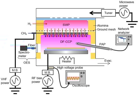
Figure 11.
Schematic illustration of the Plasma-Enhanced Chemical Vapor Deposition (PECVD) system, showing the plasma generation zone, gas inlet and exhaust arrangement, and substrate stage configuration. The system utilizes a combination of very high frequency (VHF) and radio frequency (RF) power sources to sustain the plasma and modulate ion energy, allowing precise control of film growth kinetics and microstructure. Diagnostic components such as optical emission spectroscopy (OES) and plasma absorption probes are integrated to monitor plasma behavior and reactive species during deposition [154].
PECVD also has the capacity to control film property parameters such as thickness, refractive index, hydrogen content, internal stress, and stoichiometry by manipulating a number of parameters, such as the gas composition, input power, substrate bias, pressure in the chamber, and temperature. This ability to modulate various parameters allows for an optimization for specific applications, such as the optimization of film stress to avoid crack formation in multilayer structures; many modern PECVD systems can accommodate large-sized substrates and can provide excellently uniform films over a wide area, making it a highly scalable process for industrial production [155].
Though PECVD has many advantages, it also suffers from certain drawbacks. For instance, the films deposited can have a greater amount of impurities or porosity compared to thermal CVD if parameters are not selected and controlled carefully [156]. Furthermore, plasma-induced damage to sensitive layers or devices can occur if processing at high RF powers or on thin underlying films. Still, because of low temperatures, flexibility, and ability to form complex geometries, PECVD has become a key process in the fabrication of integrated circuits, solar cells, flat-panel displays, optical coatings, as well as barrier or passivation layers in microelectronics.
4.2.4. Metal–Organic Chemical Vapor Deposition
The technique known as Metal–Organic Chemical Vapor Deposition, or MOCVD, often referred to as Organometallic CVD, is a very special way of depositing thin films. MOCVD is a specialized technique that utilizes volatile metal–organic compounds as precursors in order to deposit compound semiconductors and other advanced materials [157]. Precursors used in MOCVD are generally organometallic molecules in which metal atoms such as gallium, indium, or aluminum are chemically linked to organic ligands. When the MOCVD process occurs, the gaseous precursor is introduced into the heated reaction chamber at typically moderate temperatures (500–800 °C) and lower pressures, and decomposes or reacts on the heated substrate to form films of very high purity crystalline material. MOCVD is particularly effective for depositing III-V (e.g., GaAs, InP, GaN) and II-VI (e.g., ZnS, CdTe) compound semiconductors for which considerable industry demand exists in the production of high-speed electronics, light-emitting diodes (LEDs), laser diodes, photodetectors, and solar cells [158].
The MOCVD process enables the synthesis of high-purity, stoichiometrically controlled thin films through the decomposition of volatile metal–organic precursors on a heated substrate surface. As shown in Figure 12, the system comprises a three-part configuration: (a) the split-tube furnace, (b) the quartz reaction chamber, and (c) a schematic of the thin film growth mechanism. In this arrangement, gaseous precursors originating from the reservoir (1) are transported into the reaction chamber through a controlled gas delivery line, while a vacuum pump (2) maintains a stable sub-atmospheric pressure conducive to precursor diffusion and uniform film growth. The sealing flanges (3) and quartz tube (4) isolate the reaction environment, and the heating unit (5), supported by ceramic insulating blocks (6), sustains a uniform thermal field essential for controlled precursor decomposition.
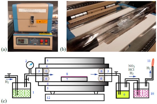
Figure 12.
Schematic representation of the Metal–Organic Chemical Vapor Deposition (MOCVD) system: (a) split-tube furnace used to generate a stable thermal environment for precursor decomposition; (b) reaction chamber arrangement showing the placement of the quartz tube and substrate zone; (c) schematic representation of the complete MOCVD workflow, including precursor delivery, heating, gas management, and by-product removal. Labeled elements: 1—precursor reservoir; 2—vacuum pump; 3—sealing flanges; 4—quartz/ceramic reaction tube; 5—heating zone; 6—ceramic insulating blocks; 7—anodic aluminum oxide (AAO) substrate; 8—Bi–Te–Ni–Cu–Au thin-film region; 9—cold-trap chamber; 10—alkaline scrubber containing sodium hydroxide solution; 11—exhaust gas torch; 12—control unit [159].
Within the hot zone, the precursor vapors decompose upon reaching the Anodic Aluminum Oxide (AAO) substrate (7), leading to the deposition of the Bi–Te–Ni–Cu–Au composite thin film (8). The by-products generated during the process are captured in a cold trap (9) and subsequently neutralized in a sodium hydroxide scrubber (10) to ensure clean exhaust flow. The gas torch (11) is incorporated for ignition and preheating of the carrier gas, while a central control unit (12) regulates parameters such as flow rate, chamber pressure, and temperature profile, providing precise process stability.
The hydrogen carrier gas serves a dual purpose—facilitating precursor transport and acting as a reducing medium to prevent unwanted oxidation during film formation. The MOCVD system’s design demonstrates an optimized deposition configuration capable of producing uniform, adherent, and compositionally tunable films for semiconductor and thermoelectric applications [159].
MOCVD, as a deposition technique, allows for a superior level of precision when controlling film stoichiometry, doping, and composition, enabling semiconductor heterostructures or quantum wells to be engineered at the atomic level. Engineering materials devices with this level of accuracy is extremely important for the purpose of controlling electronic and optoelectronic properties, such as bandgap tuning in LEDs and laser diodes. Epitaxial growth, or growth of a film that crystallographically matches the substrate, is an essential quality to achieve in order to grow high mobility and defect-free layers. MOCVD also allows for in situ doping, where n-type (silicon) and p-type (magnesium) dopants are simply characteristics of the metal–organic precursors mixed in with the film growth, allowing for seamless deposition of device layers without further processing after deposition.
The use of highly reactive and toxic metal–organic precursors such as trimethylgallium (TMGa), trimethylaluminum (TMAl), and arsine (AsH3) requires good gas handling, delivery, and safety systems with leak detection, scrubbers, and exhaust treatment, which adds complexity and cost to the operational side of an MOCVD system. The precursor chemistry also has to be selected and optimized to guarantee complete decomposition, allowing for no carbon contamination or unwanted residues to be deposited on the film [160].
Despite these difficulties, MOCVD is still the procedure of choice for commercial-scale and research growth of complex semiconductor materials on multi-layer devices because it can produce multi-layer structures that are of high quality, with excellent reproducibility and fine control. Its contribution is key to the production of blue or white LEDs (GaN); high-efficiency multi-junction solar cell technology; high electron mobility transistor (HEMT) devices; as well as photonic devices [161]. MOCVD is growing quality epitaxial films with high electrical and optical performance. All of this ensures that MOCVD will remain a key and established technique for the continued success of modern electronics and photonics [162].
Despite its exceptional chemical versatility and ability to achieve uniform film coverage, Chemical Vapor Deposition (CVD) faces inherent challenges that limit its widespread industrial adoption. The technique typically demands high substrate temperatures (600–1000 °C), rendering it incompatible with polymers and flexible materials [144]. Additionally, the reliance on hazardous and pyrophoric precursors such as silane and organometallic gases necessitates rigorous safety measures, significantly elevating environmental and operational costs [163]. The complexity of gas delivery and exhaust systems adds to capital expenses, while non-uniform gas flow can lead to thickness variations and inconsistent nucleation, compromising film quality and device reliability. Furthermore, high precursor consumption combined with slow deposition rates restricts throughput, particularly for large-area applications [164]. Consequently, although CVD offers remarkable film uniformity and compositional control, its substantial thermal requirements, precursor hazards, and high operational costs continue to impede its path toward sustainable large-scale thin film manufacturing [165].
4.3. Atomic Layer Deposition
Atomic Layer Deposition (ALD) is a sophisticated thin film deposition method that is a subclass of CVD techniques, but is unique because it grows materials one atomic layer at a time through a self-limited, sequential reaction process. The essential concept of ALD is that it is a cyclic process, in which the substrate is alternately exposed to two or more precursor gases, which react with the surface in a controlled and saturating way [166]. In a standard ALD cycle, the first precursor is pulsed into the chamber and will chemisorb to all available reactive sites on the surface of the substrate. After the purge step to remove excess precursor and by-products, the second precursor is introduced to react only with the surface-bound species, thus forming one monolayer of whichever material you desire [167]. After the one cycle is boosted by about ~0.1–0.3 nanometers of film growth, both are, the process can then be repeated again until any desired thickness is desired [168].
The PEALD process extends conventional ALD by integrating plasma activation to enhance surface reactivity and enable low-temperature film growth. As illustrated in Figure 13, the process is divided into cyclic half-reactions—each consisting of precursor dosing, purging, plasma oxidation, and surface rehydroxylation. During the first half-cycle, a volatile metal–organic precursor, such as trimethylaluminum (TMA), chemisorbs onto surface hydroxyl groups until saturation, forming a monolayer. The subsequent plasma step introduces reactive oxygen radicals that strip organic ligands, oxidize the adsorbed metal species, and regenerate active –OH sites for the next cycle [169].
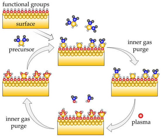
Figure 13.
Schematic representation of the Plasma-Enhanced Atomic Layer Deposition (PEALD) process showing alternate precursor and plasma exposure steps enabling atomic-level film growth [169].
The plasma component significantly improves reaction kinetics by lowering activation barriers, allowing deposition of high-density oxide films such as Al2O3 or SiO2 at temperatures well below those used in thermal ALD. The self-limiting nature of the process ensures atomic-scale control over film thickness and uniformity, while plasma activation minimizes carbon contamination and promotes superior dielectric quality. The configuration shown in Figure 13 illustrates this cyclic interaction between precursor chemisorption and plasma-assisted oxidation, which defines the fundamental mechanism of PEALD-driven conformal thin film growth.
With each surface reaction being self-limiting in ALD, this allows unrivaled control over the thickness and composition of the films on a square angstrom level. This results in films that are highly uniform, pin-hole free, and highly conformal to the surface of the substrate, even for complex 3D geometries, high aspect ratio trenches, and nanostructures, which traditional CVD could not provide. ALD is typically performed at relatively low temperatures as low as 100–300 °C, making this technique compatible with sensitive substrates and back-end processes in semiconductor manufacture. ALD is broadly capable of depositing a wide variety of materials, including metal oxides (e.g., Al2O3, HfO2, ZrO2), nitrides (e.g., TiN, AlN), sulfides, and even pure metals (e.g., Pt, Ru), depending on the chemistry associated with the precursors used.
One of the most significant benefits of ALD is the precision thickness control, which is very important in ultra-scaled semiconductor devices. In fact, ALD is the standard process to fabricate high-κ dielectric gate oxides for advanced Complementary Metal–Oxide–Semiconductor (CMOS) transistor technology, as well as barrier and capacitor layers in Dynamic Random-Access Memory (DRAM), NAND flash, and emerging memory technologies. In addition to microelectronics, ALD has growing applications in energy storage devices (e.g., Li-ion batteries), biomedical coatings, optical interference layers, and corrosion-resistant barriers due to its remarkable film quality and conformality [170]. Furthermore, area-selective ALD and PEALD are rapidly emerging options that provide additional control over film properties and process integration.
ALD and its PEALD are renowned for delivering unparalleled film uniformity and precise atomic-level control, yet these strengths inherently trade off with throughput and cost efficiency. The method’s sequential, self-limiting growth mechanism—progressing only a few angstroms per cycle—renders it impractical for thick or large-area coatings, while reliance on expensive, high-purity precursors and vacuum-based reactor systems escalates both capital and operational expenses [171]. Although plasma enhancement improves surface reactivity and allows for lower deposition temperatures, it introduces challenges such as ion-induced damage and uneven plasma distribution across larger substrates [172]. Additionally, the limited availability of suitable precursors restricts ALD’s applicability to emerging material systems. Overcoming these challenges necessitates advancements in spatial ALD and continuous-flow architectures that can accelerate deposition rates and lower costs without sacrificing the hallmark precision of the technique [173,174].
Nevertheless, there are limited drawbacks to ALD, the most prominent being a low deposition rate arising from the layer-by-layer growth of the process. This can be an issue for applications requiring thick films, unless high-throughput batch or spatial ALD systems are utilized. Furthermore, the precursors need to be chosen wisely. They need to be reactive and volatile, thermally stable, and produce minimal by-products, to ensure a clean film growth [175].
4.4. Molecular Beam Epitaxy
Molecular Beam Epitaxy (MBE) is a deposition technique performed in ultra-high vacuum (UHV) conditions, where thermally or molecularly controlled beams of elemental or sub-elemental materials are aimed at a heated crystalline substrate, promoting epitaxial growth with atomic precision in thickness, composition, strain, and doping; this precise method facilitates the production of semiconductor heterostructures and quantum devices whose efficacy is highly dependent on the quality of interfaces and levels of impurities [176].
A significant benefit of MBE is its capability to create precise interfaces with minimal intermixing, which is vital for quantum wells, dilute nitride systems, and semiconductor heterostructures. For instance, G. K. Vijaya et al. demonstrated that employing a gate-valve-activated run-vent approach along with continuous plasma operation reduces parasitic layers generated during nitrogen plasma ignition. This suppression helps to avoid n contamination in GaAs barriers and enables very sharp transitions between layers, crucial for carrier extraction and overall device performance [177].
The MBE process enables epitaxial film growth with atomic-layer precision under ultra-high vacuum (UHV) conditions (10−9–10−11 mbar), ensuring minimal contamination during deposition. As depicted in Figure 14, molecular or elemental beams from multiple effusion source ovens are thermally evaporated and directed toward a heated crystalline substrate. The substrate heater provides precise temperature control (typically 400–700 °C), promoting surface mobility for atom-by-atom crystal assembly.
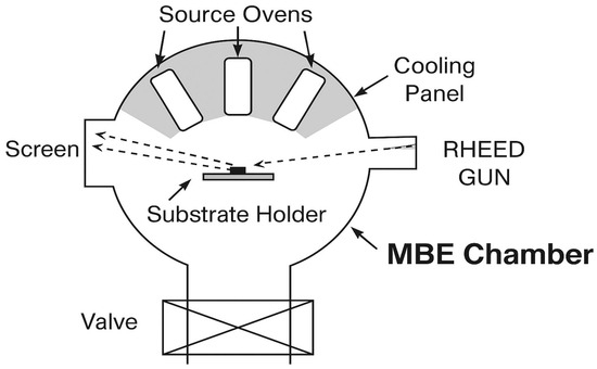
Figure 14.
Schematic illustration of a Molecular Beam Epitaxy (MBE) chamber showing the arrangement of effusion sources, substrate holder, reflection high-energy electron diffraction (RHEED) gun, and vacuum valves for ultra-high vacuum control [178].
The valve system and gate-valve-activated pumping arrangement maintain vacuum integrity and prevent parasitic reactions during material transitions, while the RHEED gun and fluorescent screen allow in situ monitoring of surface reconstruction and growth rate via diffraction patterns. Recent improvements in MBE design, such as continuous plasma operation with gate-valve-controlled run-vent cycles, have minimized parasitic layer formation during nitrogen plasma ignition, yielding abrupt and defect-free semiconductor interfaces. This combination of real-time structural control, low-energy deposition, and near-equilibrium kinetics makes MBE indispensable for fabricating III–V and II–VI compound semiconductors (e.g., GaAs, InP, CdTe) and quantum heterostructures, where interface purity and stoichiometric precision dictate device performance [178].
In quantum wells, interface disorder (such as roughness and alloy interdiffusion) has a direct impact on exciton linewidths, carrier mobility, and quantum confinement; for instance, in a study of GaAs/AlGaAs quantum wells, low-temperature photoluminescence measurements show that factors like growth temperature, V/III flux ratios, and substrate surface orientation significantly affect interface disorder, and that fine-tuning these parameters minimizes inhomogeneous broadening and enhances the quality of quantum confined states [179].
Regarding more intricate materials such as oxides, recent advancements have significantly extended the capability of Molecular Beam Epitaxy (MBE) into the domain of oxide epitaxy, incorporating approaches like suboxide MBE (S-MBE) and catalyzed variants such as Metal–Organic Chemical Atomic Layer Epitaxy (MOCATAXY). In MOCATAXY, metal–organic precursors and catalytic surface reactions are employed to achieve layer-by-layer epitaxial growth under metal–organic chemical vapor deposition-like conditions, effectively bridging the principles of MBE and MOCVD. This hybrid technique mitigates traditional oxide MBE challenges, including slow growth kinetics, source oxidation, and narrow thermodynamic growth windows, while maintaining atomic-level control over film stoichiometry and crystallinity [180].
Nonetheless, conventional elemental-source oxide MBE faces difficulties due to source oxidation: for elements that are very prone to oxidation (e.g., Sr, Ti), maintaining steady fluxes during growth in the presence of oxygen or activated oxidants (plasma, ozone) proves challenging. Crucible design, shape of the source, extended port configurations, and crucible aperture modifications have been utilized to minimize oxygen contact with the source material, thereby mitigating undesirable oxidation and enhancing flux stability [181].
Another limitation is throughput: standard oxide MBE growth rates are frequently << 100 nm/hr for numerous complex oxides, which is significantly slower than various chemical deposition techniques; this slow rate occurs due to higher fluxes or oxidant pressures that tend to disrupt stoichiometry or generate defects. Although III-V systems can achieve higher rates, the requirement for surface diffusion and kinetic management indicates that fast growth typically leads to an increase in defect density or a lack of interface sharpness [182].
MBE requires significant capital investment: UHV chambers, accurate effusion or e-beam sources, substrate heating with precise control, diagnostics (including RHEED, reflection high-energy electron diffraction; occasionally in situ X-ray diffraction, spectroscopic ellipsometry), and upkeep (source material purity, chamber bake-out, monitoring background partial pressures). The price per unit area is significantly elevated when compared to more scalable methods such as MOCVD or sputtering, particularly for larger wafer sizes [183].
From the viewpoint of heterostructure design and applications: MBE facilitates quantum wells, superlattices, delta-doping, modulation doping, and sharp barrier engineering for 2DEGs or high mobility devices; performs excellently with topological insulators such as Bi2Se3, Bi2Te3, TI/ferromagnetic or superconductor material interfaces; and for spintronic devices, owing to accurate control of spin–orbit coupling, interface roughness, and impurity scattering [184].
An emerging trade-off also exists: as one aims for increased throughput (greater growth rate, larger substrate), some accuracy diminishes—interfacial definition may worsen, defect concentrations may increase, background contaminants may integrate, or the film may release strain in less managed manners. Consequently, engineering approaches frequently require balancing deposition rate, substrate thermal conditions, and shuttering methods [185].
In conclusion, MBE continues to be the benchmark for applications needing atomic-scale control, high-purity materials, and precise interfaces; however, its limitations in throughput, scalability, and expense primarily restrict its usage to research, prototyping, and advanced device manufacturing. Future developments are expected to be found in variants such as S-MBE, catalyzed MBE, hybrid precursor-based MBE, automation, and in situ closed-loop control, along with improved design of sources and oxidation management to expand growth windows.
4.5. Pulsed Laser Deposition
Pulsed Laser Deposition (PLD) is a PVD method where high-peak-power laser pulses (typically from excimer, Q-switched Nd:YAG, or ultrafast Ti:sapphire lasers) are aimed at a solid target to generate a high-energy, transient plasma plume. The ions, atoms, clusters, and nanoparticles emitted travel several centimeters and condense on a nearby substrate, forming a thin film. The process is governed by parameters such as laser settings, background gas in the chamber, and substrate temperature; this interplay of rapid, intense energy application and ballistic transport creates the unique non-equilibrium growth conditions characteristic of PLD [186].
As illustrated in Figure 15, the Pulsed Laser Deposition (PLD) technique operates by directing a high-power, short-pulse laser beam onto a solid target inside a high-vacuum chamber, initiating localized heating, melting, and vaporization of the target material. The rapid energy transfer generates an energetic plasma plume composed of ions, neutrals, and molecular fragments that expands perpendicularly from the target surface toward the substrate. The laser fluence (1–5 J·cm−2) and pulse duration (5–20 ns) govern the ablation rate and energy distribution within the plume, which in turn influence film thickness uniformity and microstructural density.
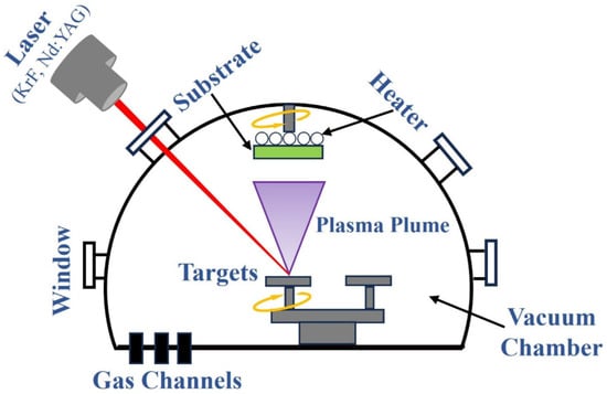
Figure 15.
Schematic of the Pulsed Laser Deposition (PLD) process showing laser–target interaction, plasma plume formation, and film growth on a heated substrate [187].
The schematic in Figure 15 depicts the core components of a PLD system, including the excimer laser, focusing lens, rotating target stage, plasma plume zone, substrate heater, and gas inlet/exhaust lines. During deposition, the substrate temperature (typically 400–800 °C) and ambient gas pressure (10−3–10−2 mbar, often oxygen or argon) are carefully adjusted to tailor plume dynamics and film stoichiometry. The ablated species condense onto the heated substrate, replicating the target composition with high fidelity, while the kinetic energy of incoming species enhances surface diffusion and promotes epitaxial alignment [187]. Compared with conventional PVD techniques, PLD offers exceptional control over stoichiometry retention, multicomponent film growth, and interface sharpness, making it particularly suitable for fabricating oxide superconductors, ferroelectrics, and 2D layered materials.
Ablation and plume physics are deeply influenced by laser wavelength, fluence, pulse duration, and repetition rate, as these factors dictate whether the target’s response is mainly characterized by photothermal melting and spallation (typical for ns pulses), by phase explosion and rapid vaporization, or by electronic excitation and picosecond–femtosecond non-thermal processes that inhibit heat diffusion; these conditions shape the kinetic energy distribution, charge state populations, and clustering behavior within the plume, which subsequently affect nucleation kinetics, adatom mobility, and the microstructure of thin films on the substrate [9].
A key engineering benefit of PLD lies in its ability to achieve quasi-stoichiometric transfer from a multi-element target to the growing film: the swift, collective ejection of material from the heated area frequently retains intricate target composition in the plume, allowing accurate deposition of multi-cation oxides and complex compounds, assuming laser fluence, background gas, and target conditions are fine-tuned to prevent preferential evaporation, self-sputtering, or light-element implantation effects that could otherwise disrupt the film’s stoichiometry [188].
PLD offers robust parameter regulation (target composition, pulse energy, and surrounding gas chemistry) and can be set up with various targets and quick target swapping, facilitating digital layer-by-layer growth methods (sequential ablation and target-rotation designs) utilized to produce superlattices, modulational doping profiles, and artificial heterostructures where compositional accuracy and sharp interfaces are crucial for device performance [9,189].
From an instrumentation and process-diagnostics perspective, PLD often incorporates in situ tools like RHEED, optical emission spectroscopy, and time-of-flight mass spectrometry to observe growth mode, stoichiometry, and plume composition in real time, enabling adjustments to growth recipes on the fly and linking process variables with atomic-scale interface quality [186].
The engineering advantages of PLD include (i) remarkable chemical fidelity for intricate and reactive chemistries through stoichiometric plume transfer, (ii) swift prototyping of novel target chemistries and multilayer structures via multi-target, sequential ablation, and (iii) the capacity to stabilize metastable phases and non-equilibrium oxidation states through precise regulation of oxygen partial pressure and substrate temperature—features that have established PLD as the preferred technique for exploratory research in complex oxides and oxide electronics [190].
Nevertheless, the practitioner must weigh these benefits against various inherent and practical constraints: a common issue is the generation and ejection of particles (droplets) from the target, which occurs due to melting, splashing, and mechanical exfoliation at the laser-target interface, causing surface defects, optical scattering, and a reduction in device yield unless addressed through velocity filters, off-axis substrate designs, customized target motion (raster/bi-directional ablation), or pulsed-beam shaping.
The creation of particulates is very responsive to laser fluence, spot quality, and pulse duration: nanosecond pulses typically facilitate the generation of larger molten ejecta and micro-droplets, while ultrashort (ps–fs) pulses diminish large droplet ejection but frequently elevate the fraction of nanoscale particles and clusters in the plume, thus making the selection of pulse regime an engineering compromise between reducing droplet size and enhancing nanoparticle influence on microstructure [191].
A further engineering limitation is lateral uniformity and scalability: due to the restricted angular extent of the PLD plume and the small target area irradiated by the laser compared to industrial wafer dimensions, thickness and compositional non-uniformities inevitably develop over large substrates; addressing this demands mechanical and optical engineering strategies (laser beam scanning, substrate movement, multiple synchronized plumes, shaped apertures, or hybrid PLD + magnetron techniques) along with precise modeling of plume geometry and particle paths to obtain wafer-scale consistency [192].
Recent methodological efforts have formalized the modeling and control strategies required for wafer-scale and 300 mm class substrates (including scanning paths, plume overlap modeling, and closed-form equations for thickness distribution); however, experimental demonstrations continue to reveal lingering non-uniformities, making PLD economically and technically difficult for high-volume manufacturing without significant innovations at the system level [193].
Throughput and expenses are additional constraints for industrial implementation: the pulsed deposition mechanism of PLD, the necessity for high-powered laser systems, durable vacuum pumping, and regular target maintenance lead to reduced area-per-unit-time deposition rates and increased Capital Expenditure/Operational Expenditure (capex/opex) relative to continuous methods (magnetron sputtering, CVD), making PLD most advantageous in value-added, low-volume, or high-functionality applications instead of bulk processing [194].
Engineers practically address the reproducibility and maintenance issues of PLD by using automated target-translation and rastering designs to reduce cone formation, employing shadow masks or velocity filters to capture large droplets, utilizing ultrafast laser regimes when suitable to manage ablation physics, and incorporating closed-loop diagnostics along with multi-physics plume models to maintain stoichiometry and interface sharpness during prolonged operations.
Regarding applications, PLD’s notable initial achievement was the deposition of epitaxial high-temperature superconducting cuprate films, where stoichiometric transfer from bulk targets enabled superconducting transition temperatures and microstructures similar to bulk specimens, thereby paving the way for superconducting thin film electronics and devices.
PLD is also extensively used for ferroelectric [195] and high-k dielectric films, where careful oxygen regulation and epitaxial strain manipulation allow for adjustment of polarization, dielectric loss, and leakage current in non-volatile memories, adjustable RF components, and integrated photonics platforms; numerous modern ferroelectric thin film demonstrations depend on PLD to achieve the necessary phase purity and epitaxial quality [196].
Aside from superconductors and ferroelectrics, PLD has played a crucial role in discovering and engineering functional oxides (perovskites, Ruddlesden–Popper phases, multiferroics, and correlated oxide interfaces) where precise control of chemistry and stress at the unit-cell level results in novel electronic and magnetic properties that bulk synthesis cannot achieve, establishing PLD as an essential research-scale instrument for oxide electronics and core condensed-matter investigations [190].
Pulsed Laser Deposition (PLD) has become a powerful research-scale tool for the fabrication of complex oxide and multicomponent thin films, yet its scalability and process control remain challenging. The technique inherently suffers from particulate ejection, target ablation non-uniformity, and plasma plume instability, all of which compromise film homogeneity and smoothness [197]. Achieving consistent stoichiometry across large substrates is difficult due to plume dynamics and substrate-target alignment. Additionally, the high-energy lasers required for ablation are costly to maintain and limit throughput to small-area substrates. Film stress and interfacial defects arising from the high kinetic energy of the deposited species can degrade mechanical and electrical properties [189]. These constraints have restricted PLD primarily to laboratory research and niche high-value applications rather than mass production. Advancements in multi-beam systems and laser scanning are ongoing to improve film uniformity and deposition scalability [198].
From an engineering roadmap viewpoint, the most viable pathways to transition PLD from discovery to application involve system-level innovations that (i) remove or filter particulates while maintaining throughput (e.g., velocity filters, bi-directional ablation, and optimized target motion), (ii) achieve wafer-scale uniformity through synchronized multi-plume designs and beam-scanning techniques, (iii) utilize ultrafast and customized pulse regimes to adjust ablation physics and minimize macroscopic ejecta while regulating nanoparticle populations, and (iv) combine advanced in situ metrology with predictive plume-to-film models for closed-loop process management [199].
In conclusion, PLD is particularly well-suited for laboratory-scale production of chemically intricate, epitaxial, and interface-sensitive thin films due to its excellent chemical fidelity and adaptable processing conditions; however, for each targeted application, a specific engineering solution must be implemented to tackle issues related to particulates, lateral uniformity, and throughput before PLD can be regarded as a preferred technique for large-scale production.
4.6. Solution-Based and Printing Methods
Solution-based and printing techniques involve a wide array of tools—such as spin-coating, dip-coating, spray deposition, sol–gel processing, inkjet printing, and slot-die/blade deposition—which prioritize industrial appeal through low capital investment and compatibility with flexible, large-area substrates, and this area has been thoroughly analyzed, focusing on materials, inks, and device categories [200]. From an engineering standpoint, each method is influenced by unique fluid-mechanical and interfacial principles: spin-coating generates a wet film that thins radially, primarily dominated by lubrication, with its ultimate thickness and solvent-evaporation trajectory regulated by angular velocity, viscosity, and volatility; comprehensive continuum models and polymer-specific models assess solvent-drag, shear thinning, and skin-formation effects that dictate the final structure [201].
As illustrated in Figure 16, the sol–gel drop-coating technique enables the controlled deposition of nanostructured thin films through a wet-chemical route involving solution chemistry and surface self-organization. In this process, a homogeneous sol precursor—typically prepared by dissolving a metal salt such as zinc acetate in an alcohol medium with a stabilizing agent (e.g., triethylamine)—undergoes hydrolysis and polycondensation to form a colloidal sol. A small volume of this sol is then dropped onto a pre-cleaned substrate surface, where gravity and capillary spreading create a uniform thin film layer. Subsequent drying and calcination (≈500 °C) remove residual organics and promote oxide network densification, resulting in a strongly adherent and crystalline coating [202].
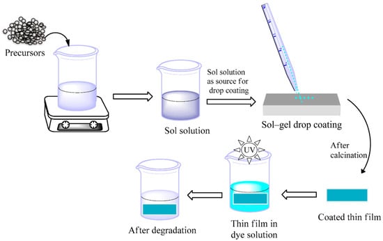
Figure 16.
Schematic representation of the sol–gel drop-coating process showing the sequential stages of sol preparation, drop deposition on the substrate, solvent evaporation, gel formation, and thermal annealing to produce a uniform oxide thin film [202].
The schematic shown in Figure 16, depicts this stepwise transformation—from precursor mixing, sol–gel preparation, and drop-casting, to gel formation, thermal treatment, and film stabilization. Such sol–gel-derived thin films offer precise stoichiometric control, low processing temperatures, and excellent compositional uniformity, making the method ideal for photocatalytic and optoelectronic oxide film fabrication. The simplicity and scalability of drop coating further allow layer-by-layer thickness adjustment, enabling the production of reproducible, defect-minimized coatings suitable for functional materials research and device integration.
Dip-coating (along with sol–gel dip methods) is governed by the Landau–Levich–Derjaguin drag-out principles in the wet phase and by the capillary/evaporation processes at the drying front, leading to withdrawal speed, solution viscosity, surface tension, and the viscoelastic properties of polymer-rich inks determining a specific film thickness and the likelihood of stratification or Marangoni-induced instabilities [203]. Spray and ultrasonic atomization techniques create polydisperse droplet plumes and temporary “wet films” on the surface, where the control of droplet size distribution, substrate temperature, and solvent evaporation rates influences nucleation-and-growth processes, thereby affecting grain size, coverage, and residual porosity in functional oxide and halide films [204].
As shown in Figure 17, the sol–gel dip-coating technique operates through a three-step sequence involving immersion, withdrawal, and solvent evaporation, each of which critically influences the final film morphology and uniformity. During substrate immersion, viscous drag and capillary forces establish a uniform sol layer on the surface, while controlled withdrawal governs film thickness via the balance between gravitational and viscous forces. Subsequent evaporation initiates the gelation stage, solidifying the layer into a continuous oxide network [124]. This process highlights how deposition parameters such as withdrawal rate, sol viscosity, and ambient humidity modulate the film’s optical and mechanical properties. Post-deposition thermal treatment (typically ≈ 400–600 °C) further drives densification and crystallization, producing compact, adherent oxide films suitable for optical, sensing, and photocatalytic applications.
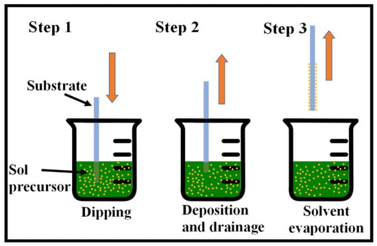
Figure 17.
Schematic representation of the sequential stages in the sol–gel dip-coating process, illustrating—Step 1: substrate immersion into the sol precursor (downward orange arrow indicating immersion), Step 2: withdrawal and drainage under controlled speed (upward solid orange arrow indicating withdrawal), and Step 3: Solvent evaporates from the deposited sol layer, initiating gelation and film formation;(upward range arrow represents solvent evaporation) [124].
Ink-based additive methods like inkjet and aerosol printing demand specific conditions for rheology, particle distribution, surface tension, and solvent evaporation, as droplet formation, ligament fragmentation, satellite reduction, and nozzle-wetting significantly affect print quality and the long-term performance of nozzles and printheads [200]. Sol–gel chemistry allows precise control at the molecular level regarding composition and facilitates the addition of dopants, templating agents, and organic modifiers, enabling the design of oxide and hybrid organic–inorganic films tailored for porosity, refractive index, and biofunctionality; the traditional sol–gel processes—hydrolysis, condensation, aging, and densification—underpin advanced coatings in biomedical and electronic fields [205].
From a processing engineering perspective, the main advantages of solution and printed methods are their suitability for low-temperature substrates, ease of compositional adjustment, and the ability for direct patterning without masks, facilitating swift materials evaluation and integration with flexible designs—elements that support recent showcases of high-performance printed perovskite solar cells and printed sensors [206].
Nonetheless, inherent constraints stem from fluid and drying irregularities: uneven solvent evaporation, concentration variations, coffee-ring effects, and surface energy discrepancies lead to inconsistent thickness, pinhole formation, and micro-voids that impair optoelectronic uniformity and device yield unless addressed through formulation or process regulation [207]. Failure modes pertinent to printing encompass particulate generation and splashing (particularly in spray techniques), nozzle blockage and satellite droplet creation in inkjet, as well as edge effects or meniscus instabilities in slot-die and blade coating—all of which correspond to measurable process windows (Weber and Ohnesorge numbers for jetting, capillary numbers, and evaporation Peclet numbers for coating) that engineers need to adhere to [204].
Developing approaches to minimize defects and enhance uniformity over large areas incorporates materials (high-grade solutes, dispersants, viscosity enhancers, and anti-aggregants), physics (regulated substrate heating, gas-flow drying, vacuum-flash annealing, and megasonic-assisted drying), and equipment (exact metering, multi-pass overlapping techniques, and closed-loop speed/flow feedback) to create dense, pinhole-free films with high production rates [206].
Regarding applications, solution and printing techniques have brought significant progress in perovskite photovoltaics as scalable deposition methods (spray, blade, slot-die, and inkjet) combined with solvent engineering and crystallization management have produced devices with laboratory-level power conversion efficiencies comparable to spin-coated cells, while also facilitating pathways to roll-to-roll production [208]. Likewise, polymer and organic electronics have gained from printed and solution techniques for organic thin film transistors, printed interconnects, and wearable sensors, since direct patterning and mechanical flexibility enable device designs that are challenging or costly to achieve with vacuum methods [200].
The sol–gel family has significantly influenced biomedical coatings: hydroxyapatite and TiO2-based sol–gel layers applied through dip or spin techniques offer adjustable bioactivity, controlled porosity, and drug-release capabilities for implant surfaces, but it is crucial to consider adhesion, sintering schedules, and thermal mismatch to prevent delamination and phase decomposition [209]. From an industrial perspective, the key challenges that persist include attaining uniformity from centimeters to meters with an acceptable level of defects, managing solvent and material handling for safety and environmental regulations, and creating inline metrology for real-time film quality (such as optical mapping, in situ Grazing-Incidence Wide-Angle X-ray Scattering/Grazing-Incidence Small-Angle X-ray Scattering (GIWAXS/GISAXS), and sheet-resistance mapping) to facilitate statistically controlled manufacturing [210].
Solution-processed and printing-based techniques—such as spin-coating, spray-pyrolysis, and sol–gel methods—are highly valued for their straightforward implementation, low-temperature processing, and adaptability to flexible substrates. However, these advantages are often offset by reproducibility issues and challenges in achieving high-quality films. Maintaining consistent film thickness and avoiding defects like pinholes, cracks, or uneven coverage is particularly difficult under ambient, uncontrolled conditions. Additionally, the dependence on solvent evaporation can lead to internal stress and non-uniform structures, frequently requiring high-temperature annealing that diminishes their cost-effectiveness [124]. In sol–gel processes, improper control of hydrolysis and condensation can result in residual porosity or unwanted impurities. Moreover, scaling up to roll-to-roll manufacturing remains constrained by difficulties in managing viscosity, adhesion, and drying behavior. Therefore, while solution-based deposition offers a promising low-cost route for flexible electronics and sensors, achieving the level of uniformity and stability needed for industrial applications demands rigorous process optimization and real-time quality control [124].
In summary, solution-based and printing technologies present an extensible engineering platform that balances cost, flexibility and materials diversity, and by combining rigorous fluid-mechanics understanding, chemistry-driven ink design, and machine-level process control it is possible to reach device performance and reliability levels required for many commercial applications—yet sustained progress will depend on integrated work across ink formulation, meniscus and drying physics, nozzle/slot hardware design, and inline defect detection to close the gap between lab-scale demonstrations and gigawatt-scale production.
4.7. Electrodeposition and Electrochemical Methods
Electrodeposition and electrochemical thin film techniques deposit substances from ionic precursors in an electrolyte onto a conductive substrate by inducing redox reactions under a specified potential or current; this essential electrochemical procedure can be performed in potentiostatic, galvanostatic, pulsed, or cyclic modes to adjust nucleation density, growth kinetics, and deposit composition at the electrode–electrolyte interface [211]. At the molecular level, deposition initiates with adsorption of solvated cations followed by heterogeneous electron transfer to form adatoms, and the interplay between interfacial mass transport (diffusion, migration, convection), double-layer charging, and surface kinetics (adatom diffusion, incorporation, and coalescence) determines whether growth proceeds by instantaneous or progressive nucleation and whether the resulting film is smooth, dendritic, columnar or porous [212].
Engineers exploit control over applied waveform—for example, using short cathodic pulses, bipolar pulsing, or reverse pulses—to decouple nucleation and growth steps so that high instantaneous supersaturation during nucleation pulses produces dense nuclei while low-current growth pulses promote lateral coalescence and improved conformality on high-aspect-ratio features [213]. Given the furnace temperature in the aluminum electrodeposition process, the alumina formed will be amorphous. Depositing nanometer-thick layers of alumina is greatly aided by electrodeposition. This electrochemical surface treatment allows for depositing thin oxide coating films made from metal salts onto different metal substrates; these coatings are typically nanoscopic, continuous, hard, corrosion-resistant, and wear-resistant. This permits conformal coating to be performed on thousands of three-dimensional architectures, including nanoporous templates, fibers, and micro-machined vias with thickness control down to 100 nm, an aspect that makes electrodeposition extremely important for conformal metallization and assembling nanowire arrays, core–shell catalysts, and through-mask patterned structures without the hassles of vacuum treatments [212].
A practical limitation in engineering is that the target of electrodeposition has to be electronically conducting in its own nature (or simply be made so, through appropriate choice of seed layers, metallization, etc.), implying that direct deposition practically remains limited to metals and highly doped semiconductors, and those surfaces which can be first pre-coated—a factor that ought to be taken into consideration when integrating with insulating device stacks [17]. Its stoichiometry and phase control of deposits consisting of even more elements (for example alloys, mixed oxides, phosphides and hydroxides) are not trivial since ionic species differ in their standard potentials, diffusion coefficients and complexation equilibria; hence, compositional tuning is usually achieved by maintaining careful electrolyte speciation, using complexing agents, controlling pH and temperature, along with the dynamic waveform strategy for the co-deposition process and suppression of preferential reduction [213].
As shown in Figure 18, electrodeposition is an electrochemical thin film growth process where metal cations in the electrolyte are driven by an applied electric field towards the cathode, where they gain electrons and are reduced to neutral atoms, forming a coherent film. The setup typically comprises an anode, cathode, and a reference electrode connected to a power source, allowing operation under potentiostatic (constant voltage) or galvanostatic (constant current) modes [214,215].
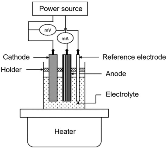
Figure 18.
Schematic representation of a standard electrodeposition setup, showing the arrangement of the cathode, anode, and reference electrode immersed in an electrolyte, connected to a power source and optionally coupled with a heater for temperature control. The configuration allows precise modulation of potential or current to facilitate thin film growth on the cathode [215].
According to Saha et al., deposition occurs primarily within the Helmholtz layer near the cathode, where cation reduction and nucleation take place, leading to film growth governed by mass transfer, diffusion, and interfacial kinetics. The process parameters—such as applied potential, electrolyte composition, temperature, and electrode spacing—strongly affect nucleation rate, grain size, and film uniformity. Incorporating a reference electrode stabilizes the working electrode potential, enabling precise control over reduction reactions crucial for stoichiometric and crystalline film formation, especially for multi-component chalcogenides like CdS, CdTe, and CZTS [215].
From the perspective of process control, additives (saccharin, thiourea, PEG, brightener, grain-refiner), agitation, rotating disk electrodes, and hydrodynamic boundary layer control are used to manipulate the transport of mass and adsorption phenomena so that the grain size of deposits can be engineered smooth or large-grained in texture and residual stresses can be engineered to meet mechanical, electrical, and catalytic specifications [216]. The technique is very good at preparing functional electrocatalysts by the direct electrodeposition of materials onto current collectors without the need for binders to adhere to the substrate. Films can be deposited hierarchically and with a large surface area, while pulsed or pulse-reverse modes provide nanostructuring opportunities for layered double hydroxides, core–shell morphologies, and even single-atom or sub-nanometer dispersions if combined with mantled dosing of precursors and post-deposition activation procedures [217].
Electrodeposition provides dense, thick coatings in microns to tens of microns for corrosion resistance, decorative, or wear-resistant metallization, with tunable microstructure and alloy chemistry. Although hard and tribological properties of the coating are improved by codeposition with inorganic particulates (ceramics, carbides, graphene), homogeneous incorporation of particles requires carefully optimized bath chemistry and controlled hydrodynamics [218]. The doctrine of electrodeposition includes being a versatile electrode fabrication methodology for energy-storage devices, since direct growth is allowed for depositing active materials on conductive current collectors, thus presenting some advantages of low interfacial resistance and improved mechanical contact, which contrasts with slurry casting of electrodes, whereas now some localized electrodeposition strategies allow for additive manufacturing of three-dimensional battery architectures with tailored porosity and tortuosity [219].
Nevertheless, there are scale-up and reproducibility issues: bath aging, impurity build-up, products of anode dissolution, and even subtle changes in complexation equilibria over time can influence deposit quality, thereby calling for inline monitoring of electrolyte composition, automated replenishment protocols, robust reference electrodes, and statistical process control to ensure uniformity in long-term production in industrial settings [213]. Recent methodological developments circumvent traditional barriers: self-terminating and site-selective electrodeposition provide atomic-scale loading control; deep-eutectic and nonaqueous electrolytes extend accessible potential window and substrate compatibility; operando characterization (in situ Raman, X-ray Absorption Spectroscopy (XAS), electrochemical quartz crystal microbalance) relates reaction intermediates and mass directly to deposition parameters, enabling closed-loop optimization [211].
In conclusion, as an array-level scaling paradigm, electrodeposition represents a tremendous opportunity for the development of conformal, compositionally tunable, and strongly adherent functional films deployed in the space between devices to deliver catalysis, corrosion resistance, and energy delivery via advanced electrodes has been demonstrated.
4.8. Hybrid and Emerging Approaches
PEALD combines plasma chemistry with the self-limiting adsorption reactions characteristic of ALD, involving a two-step cycle consisting of chemisorption of a precursor pulse onto the substrate, followed by a downstream or in-chamber plasma step that generates activated radicals or ions to facilitate completion of the surface reaction, thereby allowing film growth at much lower temperatures than thermal ALD and simultaneously preserving atomic-level control over film thickness [220].
The presence of plasma species (radicals, ions, and photons) expands the ALD process window by facilitating ligand removal, promoting densification, and enabling the deposition of materials that are hard to form thermally, which directly supports low-temperature processing on polymeric and flexible substrates where substrate thermal budgets are limited [221]. Recent engineering tests have shown that PEALD can work at temperatures close to or under 100 °C for oxide layers used in anti-reflective and protective coatings. This proves that fine-tuning plasma power pulse timing and remote-plasma setups cuts down on ion impacts while still providing enough radical flow for complete surface reactions, even on substrates that are sensitive to heat [222].
Even with these benefits, there is a built-in give-and-take between how reactive something is and how much damage it causes: high-energy ions and Vacuum Ultraviolet (VUV) light from the plasma can create surface flaws, interface states, or crosslinking in organic layers. This happens unless scientists design remote plasma setups, apply substrate biasing, or use pulsed plasma sequences to separate radical chemistry from ion bombardment [223]. From an engineering standpoint, PEALD’s readiness for flexible-electronics encapsulation and gate dielectrics depends on several factors. These include the design of reactors (with choices between remote or direct plasma, and showerhead or -coupled delivery), precursor chemistry adapted for ligand elimination at low temperatures, and process control with feedback loops. This control system links real-time optical or mass-spectrometric data to the film’s stoichiometry and electrical performance [224].
Chemical bath deposition (CBD) is a wet-chemical route in which substrate immersion in a carefully balanced solution of ionic precursors, complexing agents, and pH/temperature controls produces slow, heterogeneous nucleation and film growth at the solid–liquid interface, making CBD an inherently low-cost and scalable method for metal-oxide and metal-chalcogenide thin films [225]. The core engineering lever in CBD is control of homogeneous vs. heterogeneous precipitation: complexing ligands moderate free-metal ion activity to suppress bulk nucleation while favoring surface-mediated growth, and tuning bath chemistry, temperature, and replenishment kinetics allows thickness control from nanometers to microns across large areas [226]. Because CBD deposits by chemical reaction rather than physical arrival, it can produce high-coverage films on complex three-dimensional shapes and flexible foils and has been widely used to form buffer layers (e.g., CdS) and absorber layers (e.g., certain sulfides and selenides) in low-cost photovoltaic and optoelectronic stacks [225].
Nonetheless, the approach encounters materials-engineering issues: controlling composition in multinary systems is difficult due to varying hydrolysis and reduction potentials, bath aging and impurity accumulation can alter nucleation kinetics over time, and as-deposited films frequently need post-deposition annealing to enhance crystallinity and electronic transport, which has to be balanced with substrate thermal constraints [226]. From a practical perspective, deploying CBD on an industrial scale requires careful control of reagent metrology, inline bath speciation monitoring, recipe protocols for continuous replenishment and filtration, and integrated post-treatments (rapid thermal processing, controlled atmosphere anneals) to ensure homogeneity of the film microstructure, size distribution, and electrical properties over large areas [225].
Matrix-assisted pulsed laser evaporation (MAPLE) enhances the traditional pulsed-laser methodologies by using a volatile frozen solvent (the matrix) to be used in conjunction with the material of interest so that upon gentle laser irradiation, matrix vapor and solvated matrix species can be ejected to much more gently replace the material of interest into the substrate with far lower fragmentation compared to traditional PLD, and thus is attractive for functional organic films and bioactive coatings [227]. The fundamental physics of MAPLE, which are energy partitioning into the frozen matrix and gentle desorption of solvated macromolecules, lend insight into why chemical functionality, secondary structure, and pharmacological activity can be retained following deposition, as well as accounting for the utility of MAPLE in the deposition of dexamethasone, proteins, polymer blends, and composite biomaterials for drug-release and tissue-engineering surfaces [228].
The transfer fidelity, film density, and roughness, as well as shadow-masking or direct-write variants (MAPLE-DW) to pattern organic and biomolecular films for sensors and biointerfaces, are determined by selecting matrix, target freezing rate, laser wavelength/fluence, and substrate temperature from a process-engineering point of view [229]. Certain limitations associated with MAPLE are the throughput limitations with respect to both the pulse repetition rate and the rate of refresh for targets, the requirement to remove residual solvent or a piece of matrix (often requiring mild post-deposition anneals or vacuum drying), and the difficulty of scaling to large continuous substrates without complicated target/beam engineering [230]. In the translation towards manufacturing in the biomedical space and organic electronics, engineering approaches focused on optimized matrix chemistries that lower post-processing time, multiplexed laser heads or scanning system approaches to increase areal deposition rates, and integrated quality control (spectroscopic and bioassay methods) to provide verifiable and reproducible functional performance across production runs [227].
Roll-to-roll (R2R) deposition and coating is the primary route to continuous manufacturability of flexible thin films at scale, as it combines web handling, precise metering (slot-die, gravure, reverse-roll, spray, or flexographic printing), and thermal/UV curing in a single, continuous line capable of high areal throughput [231]. R2R methods have been modified for semiconductors, printed electronics, and barrier/functional coatings using slot-die and gravure slot-die combinations, which can achieve sub-micrometer thickness control if web tension, shim geometry, and flow rates can be processed within defined capillary and hydrodynamic process windows [232]. The primary benefits of the type of engineering involvement described here include: continuous high throughput, a low cost per unit of production at scale, and the capability to work in processing that includes multilayer, in-line processing (printing, drying, sintering/annealing, lamination, in-line metrology), which combined enable roll-to-roll manufacture of large-area photovoltaics, flexible sensors, and disposable microfluidics [233]. However, R2R comes with rigorous requirements in operating the web, such as edge wander, winding tension, and register control, drying and solvent management, as well as real-time quality assurance, because small errors in coating thickness, ink formulation, or web speed will create spatial defects that propagate downstream [234].
Thus, cutting-edge industrialization pathways have integrated near-net shape modeling (multi-physics web-coating simulations), surrogate-assisted optimization, and machine-vision/in-line metrology for thickness, electrical, and optical mapping to allow the process parameters to adaptively adjust to maintain uniformity over meters of web at high speed, all of which is capable of being undertaken in the same sensing system [235].
Table 1 aggregates representative deposition routes (PVD, CVD/MOCVD/PECVD, ALD/PEALD, MBE, PLD, solution/printing, electrochemical, spray, and hybrid variants) and juxtaposes their nominal growth rates, temperature windows, film quality attributes, and industrial adoption. Beyond listing process parameters, the table exposes mechanistic and translational patterns that guide process selection. First, a robust inverse relationship exists between growth rate and atomic/thickness precision: PVD and solution printing deliver high areal throughput but require additional engineering for conformal coating on high-aspect-ratio (AR) features, whereas ALD and Molecular Beam Epitaxy (MBE) achieve Å-level control at the cost of throughput and capital intensity. Second, thermal budget is a primary gating variable—high-temperature CVD and MBE provide epitaxy and superior crystallinity but are incompatible with polymeric or flexible substrates, creating a practical motivation for plasma-assisted or spatial ALD/CVD variants for low-T applications. Third, the table highlights methodological heterogeneity in reported metrics (e.g., growth rate units, baseline substrate conditions, and post-treatments), which reduces the validity of straight numeric comparisons; accordingly, we use the table to synthesize qualitative trends and to identify where standardization is urgently needed for cross-study meta-analysis. Finally, the rise of hybrid and additive approaches (PEALD, MAPLE, electrospray, and R2R printing) maps a clear translational pathway: seed/precision layers formed by ALD/PEALD combined with bulk, printed layers can reconcile precision with scale, and represent a promising route for flexible electronics, encapsulation, and large-area photovoltaics. The following discussion expands upon Table 1, drawing out underlying process–property correlations, methodological caveats, and areas where systematic comparative studies are most needed.

Table 1.
Detailed Overview of major deposition techniques for thin films.
Collectively, Table 1 above shows how each deposition technique provides a distinct balance between film quality, process complexity, and scalability. Physical methods such as sputtering or evaporation remain ideal for high-rate metallic coatings, while chemical and atomic layer techniques dominate when uniformity and atomic precision are essential. Solution-based and electrochemical routes, though less precise, enable low-cost and large-area fabrication. This comparison underlines that no single technique is universally superior; process choice must match the material system, substrate, and application. The table thus provides a framework for selecting deposition strategies and highlights the ongoing drive toward hybrid, low-temperature, and scalable thin film processes.
Table 2 summarizes a new generation of thin film deposition techniques that extend or hybridize conventional PVD and CVD approaches to overcome their thermal and scalability limitations. These emerging methods—ranging from plasma-assisted atomic-scale processes to additive and solution-based manufacturing—offer routes toward energy-efficient, flexible, and multifunctional coatings. In contrast to the high-temperature, vacuum-dominated routes in Table 1, the methods compiled here prioritize low-temperature operation, substrate compatibility, and functional versatility.
Table 2.
Emerging deposition methods: unique features, quantitative ranges, applications, and challenges.
A key insight is the transition from reaction rate control to surface chemistry and transport control. ALD and PEALD achieve Å-level growth through self-limiting surface reactions, enabling defect-free conformality even below 100 °C—vital for polymers and flexible substrates. MAPLE, electrospray, and inkjet printing shift toward kinetic confinement of droplets or clusters, protecting thermally fragile organics and bio-molecules while permitting direct patterning. Roll-to-roll (R2R) printing represents the scalability frontier, converting batch vacuum steps into continuous web processes. Meanwhile, chemical-bath and spray pyrolysis maintain simplicity and cost-effectiveness, albeit with higher porosity and limited microstructural control.
Together, these methods define a precision–throughput–temperature triangle: ALD/PEALD sit at the precision apex, printing and EPD at the throughput apex, and MAPLE and electrospray occupy the low-temperature axis. Understanding this balance clarifies where each technique fits in the evolving landscape of thin film manufacturing. The detailed discussion following Table 2 highlights their operational mechanisms, key advantages, and practical challenges that must be resolved for large-scale implementation.
Overall, Table 2 underscores the shift in thin film technology from purely vacuum-based, high-temperature growth toward low-temperature, additive, and hybrid approaches that merge nanoscale precision with manufacturability. Each method occupies a distinct niche: ALD and PEALD deliver atomic control; MAPLE and electrospray preserve molecular integrity; printing and EPD enable scalable, low-cost production. The common challenge is achieving uniformity and reproducibility while retaining functional performance. As research progresses, combining these methods—for example, ALD seed layers followed by printed or electrochemical over-layers—appears to be the most promising strategy for uniting precision, scalability, and sustainability in next-generation thin film fabrication.
5. Classification and Material Properties
5.1. Composition-Based
Thin films are commonly categorized according to their composition, structure, or functional characteristics, each of which plays a defining role in determining their performance across diverse applications. In composition-based classification, emphasis is placed on the elemental or compound makeup of the film, as this directly governs its electrical, optical, and mechanical properties. The interplay between intrinsic material attributes, processing parameters, and interface quality ultimately dictates the film’s overall behavior and its suitability for specific technological purposes.
5.1.1. Metallic Thin Films
Thin metallic films, including copper (Cu), silver (Ag), gold (Au), and aluminum (Al), are mainly noted for their excellent electrical and thermal conductivity attributed to their free electron gas properties. The metallic bonds provide ductility, strong adhesion to different substrates (with suitable surface preparation), and outstanding reflectivity in the infrared and visible wavelengths. Copper and silver, specifically, are extensively utilized as interconnect layers in microelectronics, transparent conductive layers in optoelectronic devices, and as reflective coatings in optics [263]. Metals are prone to oxidation (e.g., Cu forming Cu2O), potentially diminishing performance; thus, protective capping layers or regulated deposition conditions are typically necessary. In metallic thin films, the size of grains, crystallographic orientation, and density of defects can significantly affect resistivity, resistance to electromigration, and mechanical durability [264].
5.1.2. Semiconductor Thin Films
Semiconductors like silicon (Si), gallium arsenide (GaAs), and new two-dimensional materials such as molybdenum disulfide (MoS2) are fundamental to contemporary electronics and optoelectronics. Their usefulness comes from an adjustable band gap, enabling regulated electrical conductivity via doping and defect manipulation [265]. Thin film silicon is widely utilized in photovoltaics, display backplanes, and sensors, whereas compound semiconductors such as GaAs provide enhanced electron mobility and direct bandgap characteristics for high-frequency and optoelectronic uses. Transition metal dichalcogenides (TMDs), like MoS2, offer extra advantages such as atomic-scale thickness, elevated on/off ratios in field-effect transistors, and adaptability for wearable devices. Techniques like CVD and molecular beam epitaxy (MBE) allow for precise control over film stoichiometry, crystallinity, and interface quality, all of which are essential for device reliability [266].
5.1.3. Dielectric Thin Films
Dielectric films with materials like silicon dioxide (SiO2), hafnium oxide (HfO2), aluminum oxide (Al2O3), and titanium dioxide (TiO2) are prized for their significant electrical resistivity and capability to retain electrical charge without allowing conduction. They function as gate dielectrics in transistors, insulating barriers in capacitors, and anti-reflective or protective layers in optics. SiO2 continues to be the most commonly utilized dielectric because of its compatibility with silicon technology, thermal stability, and favorable interface characteristics [266]. High-k substances such as HfO2 are being adopted more frequently to substitute SiO2 in modern CMOS devices, facilitating additional miniaturization and managing leakage currents. The dielectric constant, breakdown strength, and defect density are vital factors, and accurate management of thickness uniformity is crucial for reliable operation in large-area devices [267].
5.1.4. Polymeric Thin Films
Thin films based on polymers, including poly (3,4-ethylenedioxythiophene) polystyrene sulfonate (PEDOT:PSS), polyimides, and fluoropolymers, provide flexibility, lightweight properties, and convenient solution processing. These substances are especially appealing for flexible electronics, organic solar cells, and wearable detectors [268]. PEDOT:PSS, for instance, merges electrical conductivity with optical clarity, rendering it appropriate for transparent electrodes. Polymeric thin films typically show diminished thermal stability and mechanical strength in comparison to inorganic films; however, they can be modified with additives, crosslinking, or hybrid approaches to enhance their durability. The molecular structure, chain arrangement, and level of crystallinity can be adjusted during deposition to enhance performance for particular applications [269].
5.1.5. Hybrid and Emerging Thin Films
Hybrid thin films integrate the characteristics of organic and inorganic materials to obtain multifunctionality. Instances comprise halide perovskites (such as CH3NH3PbI3), MXenes (two-dimensional transition metal carbides or nitrides), and metal–organic frameworks (MOFs). Perovskite thin films have attracted considerable interest in photovoltaics because of their high absorption coefficient, adjustable band gap, and extended carrier diffusion lengths [270]. MXenes demonstrate excellent electrical conductivity, water affinity, and adjustable surface chemistry, positioning them as ideal candidates for energy storage and electromagnetic shielding. MOF thin films provide significant porosity and selective chemistry, facilitating uses in sensing and gas separation. These new materials frequently encounter issues with environmental stability and large-scale production, yet continuous research in encapsulation, scalable deposition, and defect passivation is gradually enhancing their practicality [271].
5.1.6. Interdependence of Material Properties
Thin film performance, irrespective of classification, is determined by a combination of inherent material characteristics and external factors introduced during the manufacturing process. Intrinsic characteristics encompass electronic configuration, lattice parameter, thermal expansion rate, and optical absorption spectrum. Extrinsic factors encompass grain boundaries, impurities, stress in the film, and the quality of interfaces. For example, the resistivity of a metallic film can be greatly influenced by nanoscale grain size, whereas a dielectric film’s breakdown voltage is affected by defect density. This renders the choice of deposition methods, substrate preparation, and post-deposition treatments essential steps in guaranteeing that the desired material properties are realized [272].
In summary, composition-based classification offers a rational approach for choosing thin films for particular uses. Metals are superior conductors, semiconductors allow device operation, dielectrics offer insulation and charge retention, polymers contribute flexibility, and hybrids provide customized multifunctional capabilities. Grasping the basic material characteristics as well as the variations caused by processes is crucial for creating high-performance thin film systems in various technological fields.
5.2. Structure-Based
Thin films may also be categorized based on their structural arrangement, which significantly influences their mechanical, electrical, thermal, and optical properties. Composition establishes the essential components of a film, while its structure—be it amorphous, crystalline, or a hybrid nanocomposite—dictates the spatial arrangement of these atoms and their interactions at the micro- and nanoscale. Consequently, structural classification is essential for customizing films to meet particular functional needs in electronics, optics, energy devices, and protective coatings.
5.2.1. Amorphous Thin Films
Amorphous thin films do not possess long-range atomic organization, with atoms positioned in a disorganized manner akin to glass. The lack of periodicity removes grain boundaries, resulting in isotropic characteristics throughout the film. Substances like amorphous silicon (a-Si), amorphous carbon, and amorphous metal oxides (e.g., indium gallium zinc oxide, IGZO) are extensively utilized in applications where consistency and smoothness are vital [273]. Amorphous films typically display high optical clarity, consistent electrical properties across extensive areas, and improved resistance to corrosion thanks to the lack of grain-boundary diffusion routes. IGZO thin films act as active layers in thin film transistors utilized in display technologies, providing low leakage currents and consistent performance. Nonetheless, the absence of crystalline structure may restrict carrier mobility and thermal conductivity, rendering amorphous films better suited for low-temperature, expansive applications rather than high-speed electronics [274].
5.2.2. Crystalline Thin Films
Crystalline thin films exhibit long-range atomic order, featuring atoms organized in a consistent lattice. They can be categorized into single-crystalline and polycrystalline types. Single-crystalline thin films exhibit a consistent lattice orientation across the entire material and are generally fabricated epitaxially on substrates that match the lattice. These films demonstrate enhanced electrical conductivity, improved carrier mobility, and greater mechanical strength due to low defect density. They are essential in high-performance microelectronics, optoelectronic devices, and sensors, where accurate control of electronic band structure is crucial [275]. Polycrystalline thin films, in contrast, are made up of many crystallites divided by grain boundaries. Although grain boundaries can impede carrier movement and decrease conductivity, polycrystalline films are simpler to produce in large quantities and at a lower cost. Grain size, texture, and crystallographic orientation greatly influence the functional properties. For example, polycrystalline titanium nitride (TiN) layers provide excellent hardness and wear resistance, whereas polycrystalline silicon is an essential material for thin film solar panels and MEMS [275].
5.2.3. Nanocomposite Thin Films
Nanocomposite thin films merge two or more different phases—typically blending crystalline and amorphous parts—at the nanometer scale to obtain multifunctional characteristics. The incorporated nanostructures may be metallic, ceramic, polymeric, or carbon-based, and are generally distributed within a continuous matrix. This combined framework facilitates synergistic improvements in properties, like better hardness without compromising toughness, higher electrical conductivity in typically insulating matrices, or improved thermal stability [276]. Metal–dielectric nanocomposites can demonstrate adjustable plasmonic behaviors, facilitating sophisticated optical sensors and filters. In the same way, ceramic–metal nanocomposites can merge wear resistance with electrical conductivity for triboelectric uses. The phase interface in nanocomposites is crucial for performance, as it can serve as a barrier to dislocation movement, a location for electron scattering, or a route for ion transport. Thus, regulating the dimensions, morphology, and arrangement of the embedded nanostructures is crucial for enhancing their properties [277].
5.3. Functionality-Based
Thin films may also be categorized based on their functional roles in devices and systems, as dictated by their inherent and designed physical characteristics. This classification based on functionality is especially pertinent in applied research and product development, where materials are chosen not only for their composition or structure but also for the particular operational role they serve. Four major functional categories—conductive, optical, ferroelectric, and catalytic—highlight essential technological areas where thin films are crucial.
5.3.1. Conductive Thin Films
Conductive thin films are created to enable the effective movement of electrical current while ensuring stability, adhesion, and sometimes transparency. Their electrical properties can be metallic, semiconducting, or ionic, based on the type and density of carriers. Conductive metallic films like copper (Cu), silver (Ag), and aluminum (Al) are widely employed as interconnects, electrodes, and shielding layers because of their excellent conductivity and compatibility with various processes [278]. Transparent conductive oxides (TCOs), like indium tin oxide (ITO) and aluminum-doped zinc oxide (AZO), merge conductivity with optical clarity in the visible range, making them suitable for use in touchscreens, displays, and solar cells. The effectiveness of conductive thin films is affected by factors like grain size, surface roughness, defect density, and film thickness, which can be improved by choosing appropriate deposition methods and using post-deposition processes such as annealing [279].
5.3.2. Optical Thin Films
Optical thin films are designed to manage light transmission, reflection, absorption, or emission by carefully adjusting their refractive index and thickness. These films are essential for lenses, mirrors, photonic devices, and energy systems. Dielectric films like silicon dioxide (SiO2), titanium dioxide (TiO2), and magnesium fluoride (MgF2) are employed for anti-reflective coatings, high-reflectivity mirrors, and interference filters [168,280]. In photonics, multilayer optical stacks are engineered to attain wavelength-selective characteristics via constructive and destructive interference. Optical thin films need to demonstrate excellent transparency, low scattering, and resistance to environmental factors, particularly for outdoor or high-power laser uses. Techniques like PVD and ALD provide angstrom-scale regulation of thickness, facilitating exact adjustments of optical behaviors. Flaws, impurities, or inconsistencies in thickness can greatly impair optical performance, rendering process control essential [281].
5.3.3. Ferroelectric Thin Films
Ferroelectric thin films exhibit spontaneous electric polarization that can be altered through the application of an external electric field. This distinctive feature, resulting from a non-centrosymmetric crystalline arrangement, facilitates uses in non-volatile storage, piezoelectric drivers, electro-optic switches, and energy collectors. Typical ferroelectric materials consist of lead zirconate titanate (PZT), barium titanate (BaTiO3), and compounds based on hafnium oxide [282]. The performance of ferroelectric thin films is highly influenced by their crystalline orientation, domain configuration, and the quality of the interface with electrodes. In memory applications, the endurance of polarization states and resilience to fatigue during multiple switching cycles are essential performance metrics. Incorporating ferroelectric thin films into semiconductor platforms demands precise management of leakage currents, interface traps, and mechanical stress to ensure dependable performance [282].
5.3.4. Catalytic Thin Films
Catalytic thin films increase the speed of chemical reactions without losing their effectiveness, providing high surface-area-to-volume ratios and adjustable surface chemistry in comparison to bulk catalysts. They find applications in heterogeneous catalysis, electrochemical energy transformations, and environmental cleanup. Thin films of noble metals like platinum (Pt), palladium (Pd), and ruthenium (Ru) are extensively used in fuel cells, hydrogen generation, and automotive emissions treatment [283]. Thin films of transition metal oxides such as TiO2, Co3O4, and NiO are used in photocatalysis to degrade pollutants and facilitate solar-driven water splitting. The efficacy of thin films as catalysts is influenced by surface architecture, defect locations, grain interfaces, and chemical makeup, all of which can be adjusted via deposition conditions, doping, or treatments after deposition. Nanostructuring the surface of the film can substantially elevate the density of active sites, thereby improving catalytic performance [283].
5.4. Dimensionality
Thin films can additionally be categorized based on their dimensional characteristics, which pertain to their physical thickness, the quantity of superimposed layers, and the degree of confinement experienced by electrons, phonons, and photons within the substance. Dimensionality significantly affects the physical characteristics of a film, frequently resulting in behaviors that vary greatly from those of the bulk material. By manipulating thickness and layer configuration at the nanoscale, one can customize electronic, optical, thermal, and mechanical properties for specific uses. Four primary dimensional categories—ultrathin, two-dimensional (2D), multilayer, and superlattice structures—embody different design approaches in thin film science.
5.4.1. Ultrathin Films
Ultrathin films are generally characterized by thicknesses in the range of a few nanometers or less, nearing the dimensions of a few atomic layers. Under this regime, surface and interface effects prevail over bulk characteristics, and quantum size effects can greatly influence electrical conductivity, optical absorption, and magnetic properties. For instance, the band gap and work function of a semiconductor may change because of electron confinement within a very thin layer [284]. Ultrathin metallic layers frequently display elevated resistivity because of increased electron scattering at both surfaces and grain boundaries, whereas dielectric ultrathin layers serve as tunneling barriers in nanoscale electronic devices. Creating continuous and flawless ultrathin layers demands accurate regulation of deposition parameters, since incomplete coverage or island formation can undermine uniformity and effectiveness [285,286].
5.4.2. Two-Dimensional (2D) Films
Two-dimensional films are atomically thin crystalline structures, typically just a single unit cell in thickness, exhibiting strong in-plane bonding and weak van der Waals interactions between layers. Instances comprise graphene, hexagonal boron nitride (h-BN), and transition metal dichalcogenides (TMDs) like molybdenum disulfide (MoS2) and tungsten diselenide (WSe2). These materials demonstrate outstanding electronic, optical, and mechanical characteristics stemming from their lower dimensionality, such as elevated carrier mobility, direct band gaps in monolayer TMDs, and remarkable flexibility [287]. The absence of dangling bonds at surfaces enables clean interfaces, benefiting the fabrication of heterostructures. Nonetheless, producing high-quality 2D films over large areas continues to be difficult, as techniques like CVD and mechanical exfoliation present compromises between scalability and crystalline quality [287].
5.4.3. Multilayer Films
Multilayer films consist of a series of unique thin film layers, frequently alternating between various materials, to merge or improve functional characteristics. These layers may vary from a few nanometers to several hundred nanometers thick, based on the desired application [288]. Multilayer structures are commonly employed in magnetic storage devices (e.g., giant magnetoresistance stacks), optical coatings (e.g., broadband reflectors or anti-reflective coatings), and barrier films (e.g., diffusion-resistant layers in packaging or electronic applications) [288]. The effectiveness of multilayer films relies on the quality of each layer, the clarity of interfaces, and the extent of lattice compatibility between materials. Interdiffusion, the buildup of stress, and the creation of defects at interfaces are crucial elements that can influence long-term stability [288,289].
5.4.4. Superlattice Films
Superlattices represent a unique type of multilayer structure where two or more materials are stacked alternately with periodic thicknesses at the scale of several atomic layers [290]. The periodic structure and interface characteristics in superlattices result in the emergence of novel electronic and phononic band structures that do not exist in the individual constituent materials [290]. This may lead to new phenomena like improved thermoelectric efficiency from phonon scattering at boundaries, customized band gaps for optoelectronic uses, or designed magnetic interactions for spintronic technologies. Semiconductor superlattices (e.g., GaAs/AlAs) have been utilized to form high-mobility quantum wells, whereas oxide superlattices can display emergent characteristics like interfacial ferroelectricity or magnetism. Attaining the exact periodicity and sharp interfaces needed for superlattice functionality generally requires sophisticated deposition methods like molecular beam epitaxy (MBE) or pulsed laser deposition (PLD) [291].
5.4.5. Interrelation of Dimensional Regimes
The dimensionality classifications are not completely separate; ultrathin films can exhibit 2D characteristics, while multilayer films can be designed as superlattices by managing their periodicity. The selection of a dimensional regime relies on the interplay between targeted physical outcomes, manufacturing practicality, and application limitations. For instance, ultrathin 2D films are outstanding in flexible electronics, whereas multilayers and superlattices lead in precision optical filters, magnetic devices, and thermoelectric modules [292].
Dimensional engineering serves as a robust resource in thin film technology, facilitating characteristics that cannot be achieved in bulk substances. Ultrathin films utilize quantum and surface phenomena, 2D films exhibit remarkable intrinsic attributes at the atomic level, multilayers enable functional consolidation, and superlattices generate completely new states of matter via periodic arrangements. Expertise in deposition methods, interface management, and thickness accuracy is crucial to maximizing the capabilities of these dimensional ranges in advanced devices.
Table 3 consolidates thin films across all major material classes—metals, dielectrics, semiconductors, organics, hybrids, 2D materials, and functional oxides—linking their intrinsic properties with deposition strategies and technological roles. Beyond classification, the table reveals how performance metrics such as conductivity, bandgap, transparency, and functionality are closely coupled to both composition and processing route. Metallic films remain the foundation for interconnects and plasmonic devices due to their high carrier densities and reflectivity, whereas dielectric and oxide films enable insulation, passivation, and optical control through wide bandgaps and high breakdown fields. Semiconducting layers, both inorganic (Si, CdTe, CIGS, perovskites) and amorphous-oxide (a-IGZO), underpin modern electronics and photovoltaics, where mobility, defect control, and stoichiometric uniformity dictate device efficiency.
Table 3.
Classification of thin films by material class, functionality, thickness, and applications.
Organic and hybrid films bridge mechanical flexibility and functional tunability, offering lightweight and low-temperature processability but suffering from moisture sensitivity and limited thermal stability. Two-dimensional (2D) crystals such as graphene and MoS2 extend this trend toward atomically thin, quantum-confined systems, introducing high carrier mobility and exotic interfacial physics. Ferroelectric, magnetic, superconducting, and topological films represent specialized functional classes whose properties are dominated by crystallographic orientation, strain, and thickness—parameters strongly governed by deposition technique. The table thus functions not merely as a taxonomy but as a structure–process–property–application map, exposing how advances in synthesis directly translate into emerging device domains.
Collectively, Table 3 illustrates that thin film technology has evolved from single-function coatings to a vast ecosystem of multifunctional materials spanning electronics, energy, photonics, and biomedicine. Each category embodies a specific trade-off between structure, processing temperature, and functional performance. Metals and dielectrics define the electrical and optical backbone of modern devices; semiconductors and 2D materials supply tunable electronic behavior; functional oxides, polymers, and hybrids add adaptability, flexibility, and responsiveness. No single deposition technique suffices across this diversity—hence the increasing emphasis on combinatorial and hybrid approaches, where ALD, sputtering, and solution processing are sequentially integrated. The table therefore serves as both a classification framework and a roadmap linking material selection, processing method, and target application in next-generation thin film systems.
6. Applications of Thin Films
6.1. Electronics and Photonics
Thin films are essential in electronics and photonics because they provide accurate control over electrical, optical, and structural characteristics at micro- and nanoscale levels. Their diminished thickness, along with sophisticated deposition methods, enables tailored functionalities that bulk materials are unable to offer [317]. In electronic devices, thin films act as both active materials for signal processing and as passive layers for insulation, protection, or optical modulation. In photonics, they function in regulating light propagation, reflection, and emission by utilizing customized refractive indices, band gaps, and surface structures [168].
Thin films are utilized in transistors for semiconductor channels as well as dielectric gate oxides. Thin film transistors (TFTs) utilize materials including amorphous silicon, polycrystalline silicon, or new oxide semiconductors such as IGZO (indium gallium zinc oxide) to enable affordable, large-area electronics [318]. The thin film structure enables lower parasitic capacitance, improved electrostatic control, and compatibility with flexible substrates. These devices are vital for displays, sensors, and low-energy logic applications, where consistent performance across extensive areas is crucial. The application of ultra-thin high-k dielectrics like hafnium oxide further improves transistor scaling while preserving low leakage currents [319].
As illustrated in Figure 19, the ambipolar organic thin film transistor (OTFT) gas sensor utilizes a Poly(naphthalene diimide–bithiophene)-PNDTI-BT-based active layer capable of dual carrier modulation. The molecular design of PNDTI-BT, shown in Figure 19a, incorporates naphthalenediimide and bithiophene units that facilitate balanced electron and hole mobility under ambient conditions. The schematic in Figure 19b details the bottom-gate, bottom-contact configuration, comprising a multilayer stack of Si/SiO2/Al2O3/Au/PNDTI-BT/Au, which ensures stable operation due to the high dielectric constant of the Al2O3 layer and its interface compatibility with organic semiconductors [320].
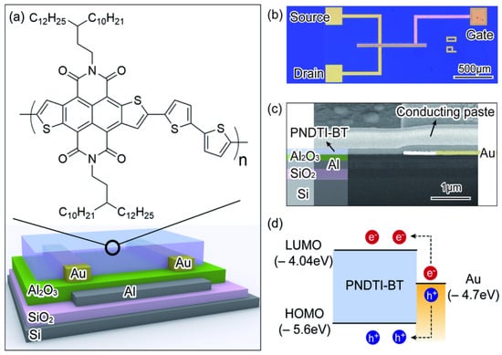
Figure 19.
Schematic illustration of the ambipolar organic thin film transistor (OTFT) gas sensor based on the PNDTI-BT active layer. (a) Molecular structure of PNDTI-BT and schematic device architecture showing the multilayer configuration (Si/SiO2/Al/Al2O3/Au). (b) Optical microscopy top-view image of the fabricated OTFT, highlighting the source, drain, and gate electrodes. (c) Cross-sectional scanning electron microscopy (SEM) image of the device showing the layered structure and conducting paste contact. (d) Energy band diagram illustrating the junction between the PNDTI-BT active layer and the Au source/drain electrodes [320].
The optical and SEM images (Figure 19c) confirm the high-quality film morphology and the well-defined interfaces between the dielectric and active layers, essential for minimizing charge-trap states and improving channel uniformity. The energy band diagram in Figure 19d further illustrates the HOMO (–5.6 eV) and LUMO (–4.04 eV) alignment with gold electrodes, producing low injection barriers for both charge carriers and enabling efficient ambipolar transport. This configuration allows gate-tunable modulation of carrier type—critical for chemiresistive sensing, where the drain current varies distinctively under oxidizing (NO2) and reducing (NH3) atmospheres [320].
Such architecture demonstrates how organic thin film transistors can function not only as switching devices but also as gas sensors with programmable polarity and high selectivity, establishing a bridge between flexible electronics and environmental sensing technologies.
In memory devices, thin films facilitate high-density data storage by managing charge or magnetic states at the nanoscale. Non-volatile memories like resistive RAM (RRAM), phase-change memory (PCM), and magnetoresistive RAM (MRAM) all rely on thin films to create operational switching layers [321]. These films typically measure only a few nanometers in thickness, enabling rapid switching speeds and minimal energy usage. In DRAM, extremely thin dielectric layers dictate the capacitance and consequently the storage capacity of every memory cell. Thin films enhance data retention and minimize degradation in storage devices by accurately managing defect densities and the quality of interfaces [322].
In optical coatings, thin layers are created to control light transmission, reflection, and absorption. They are used in anti-reflective coatings for lenses, beam splitters, and laser optics, where various layers of regulated thickness create interference effects to attain the desired optical performance. Dielectric mirrors with high reflectivity, utilized in lasers and interferometers, consist of layers of thin films with alternating high and low refractive indices [323]. These coatings can also act as protective barriers against environmental deterioration of optical components [323].
In light-emitting diodes (LEDs) [324] and organic light-emitting diodes (OLEDs) [325], thin films create the emissive layers where photon production occurs through electron-hole recombination. In inorganic LEDs, emission wavelength and efficiency are determined by epitaxially grown thin films of gallium nitride (GaN) or similar compounds [324]. In OLEDs, organic thin films are layered meticulously for charge transport, light emission, and encapsulation [325]. The thin film design allows for high pixel densities, reduced power usage, and flexibility, rendering them appropriate for cutting-edge display technologies.
Display technologies depend significantly on thin films for both functional and structural roles. Liquid crystal displays (LCDs) [326] utilize thin film transistor arrays to manage individual pixels, whereas OLED and micro-LED displays [327] implement thin films for both active emission and encapsulation. Transparent conductive thin films like ITO offer electrical conductivity while maintaining optical transparency, allowing for touchscreens and see-through display panels. Additionally, the capability to apply thin films onto flexible polymer substrates has created opportunities for displays that are rollable, foldable, and wearable [328].
In conclusion, thin films in electronics and photonics provide an unparalleled combination of miniaturization, performance enhancement, and integration adaptability compared to bulk materials. Their function ranges from active semiconducting layers in memory and logic to optical coatings and emission layers in photonics. The exact regulation of thickness, microstructure, and composition allows for custom properties that satisfy the rigorous requirements of contemporary electronic and optical systems. As device designs advance towards increased density, versatility, and multifunctionality, thin films will remain a fundamental driver of innovation in both areas.
6.2. Energy
Thin films are essential in contemporary energy technologies, facilitating lightweight, efficient, and scalable options for energy harvesting, storage, and conversion. The distinct characteristics they possess, including adjustable band gaps, elevated surface-to-volume ratios, and the capability to be integrated onto flexible or non-traditional substrates, render them perfect for applications where efficiency, cost, and form factor are essential. In the energy industry, thin films play a crucial role in solar cells, thin film batteries, and fuel cells, where they impact performance, longevity, and production viability directly [329].
In photovoltaic (PV) systems, thin films are utilized to capture sunlight and transform it into electricity. Thin film solar cells need much less active material compared to conventional crystalline silicon wafers, leading to lower production costs and enabling deposition on flexible substrates. CdTe solar cells rank among the most commercially viable thin film photovoltaic technologies. CdTe provides an almost ideal bandgap for solar absorption and can be applied through scalable techniques like close-spaced sublimation [330]. CIGS solar cells represent a significant technology, merging elevated absorption coefficients with adjustable band gaps through modification of the Ga/In ratio. This adjustability enables fine-tuning for various lighting situations [331]. New perovskite solar cells, utilizing hybrid organic-inorganic halide thin films, have demonstrated swift improvements in efficiency over the past few years. They provide low-temperature solution processing and are compatible with flexible substrates, but challenges persist regarding stability and long-term degradation [332].
As illustrated in Figure 20, El-Amin and Ibrahim developed an (Al + Ag)/n+-Si/p-Si/Al thin film silicon solar cell using a linear facing target sputtering (LFTS) technique, enabling the deposition of uniform, microcrystalline Si layers at low substrate temperatures. This structure features a glass substrate coated with Al and Ag as a reflective back electrode, followed by a p-type μc-Si absorber and an n+-Si emitter layer forming the p–n junction. The top Al contact functions as a transparent conductive electrode for efficient photon coupling and charge extraction. The study demonstrated that optimizing film thickness is crucial for balancing optical absorption and recombination behavior. Electrical characterization showed that reducing the cell thickness improves the open-circuit voltage (V_OC) due to reduced bulk recombination; however, excessive thinning increases surface recombination losses, necessitating controlled texturing and surface passivation. The absorbed photon flux density was found to be three times higher at the interfaces of thinner films, confirming enhanced light trapping and carrier generation near the surface. Moreover, the inclusion of the Al interfacial layer acted as a multifunctional buffer, improving grain growth and serving as an ohmic back contact [333].
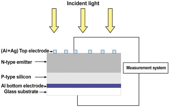
Figure 20.
Schematic Diagram of a thin film Si solar cell [333].
These results underline how sputtered μc-Si thin film architectures can achieve high absorption efficiencies and cost-effective scalability while preserving structural and electrical integrity—marking an advancement toward flexible, low-cost thin film photovoltaic technologies.
Thin films improve energy storage in thin film batteries, essential for compact, lightweight power sources in portable electronics, medical implants, and IoT devices. These batteries employ thin film electrodes and solid electrolytes to attain elevated energy density, extended cycle life, and minimal self-discharge rates [334]. Typical electrode materials consist of lithium cobalt oxide (LiCoO2) for cathodes and lithium phosphorus oxynitride (LiPON) for solid electrolytes. The thin film configuration enables accurate regulation of layer thickness, enhancing ion movement and facilitating quicker charge–discharge cycles. Additionally, the capability to apply coatings on flexible or uneven surfaces broadens their applicability in wearable and integrated technologies [335].
In fuel cells, thin films play a role in the effective electrochemical transformation of fuels into electricity. Thin film electrolytes in solid oxide fuel cells (SOFCs), like yttria-stabilized zirconia (YSZ), enhance ionic conduction at reduced temperatures when produced in very thin layers. Decreasing the operating temperature enhances longevity and reduces material expenses [336]. In a similar manner, thin film catalyst layers within proton exchange membrane fuel cells (PEMFCs) improve reaction kinetics while reducing the consumption of valuable metals such as platinum. Accurate deposition techniques like ALD or sputtering facilitate consistent catalyst distribution and enhance electrode functionality [337].
The incorporation of thin films in energy systems allows for innovative device designs. Tandem solar cells integrate various thin film materials to harness a wider range of sunlight, greatly enhancing conversion efficiency. Flexible thin film PV modules can be incorporated into building exteriors, automobiles, or wearable technology, combining energy production with structural or design elements [338]. In energy storage, microfabricated thin film batteries can be directly integrated onto circuit boards or sensors, removing the necessity for large external power sources. In fuel cells, electrodes supported by thin films facilitate compact, portable power systems for unmanned devices or remote use [339].
In general, utilizing thin films in the energy industry offers a route to achieve more efficient, compact, and flexible energy solutions. Thin films tackle the primary issues of cost, weight, and integration in renewable energy and storage technologies by facilitating scalable manufacturing, compatibility with flexible substrates, and improved functional performance. With advancements in deposition methods and enhanced material stability, thin films will remain essential in the shift towards cleaner and more sustainable energy systems.
6.3. Sensors and Biomedical
Thin films are becoming increasingly significant in sensor and biomedical fields due to their elevated surface-to-volume ratios, adjustable material characteristics, and ability to interact efficiently with chemical, biological, and physiological environments. Their ultra-thin design allows for quick signal response, elevated sensitivity, and incorporation into small or flexible devices [340]. In gas sensing and biosensing, thin films serve as functional layers that engage directly with the target analyte, resulting in detectable changes in electrical, optical, or chemical signals. In biomedical applications, thin films are utilized as biocompatible coatings, protective barriers, and layers for controlled drug release, broadening their use from sensing to therapeutic and diagnostic functions [340,341].
As depicted in Figure 21, Sureshkumar et al. described the chemiresistive mechanism governing metal-oxide thin film gas sensors, which operate via surface adsorption and charge-transfer phenomena. In ambient air, oxygen molecules chemisorb onto the semiconductor surface as negatively charged species (O−, O2−, O22−), extracting electrons from the conduction band and forming a depletion layer. When exposed to reducing gases (e.g., CO, H2, NH3), these adsorbed oxygen ions react with the gas molecules, releasing electrons back into the semiconductor and thereby decreasing resistance. Conversely, oxidizing gases (e.g., NO2, O3) further withdraw electrons, expanding the depletion width and increasing resistance.
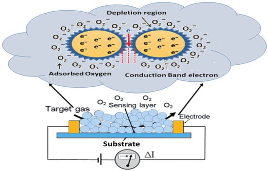
Figure 21.
Schematic representation of the working principle of a metal-oxide thin film gas sensor. The diagram illustrates the adsorption of oxygen species (O−, O2−) on the metal-oxide surface, the formation of a depletion region, and the subsequent modulation of the conduction band in response to target gas molecules [342].
The sensitivity and response dynamics of such sensors are primarily governed by film morphology, crystallite size, porosity, and operating temperature. Nanostructured oxides like ZnO, SnO2, and TiO2 provide superior performance due to their high surface-to-volume ratio, enabling a dense distribution of active adsorption sites that accelerate surface reactions. Moreover, dopants or noble metal nanoparticles (e.g., Pt, Pd, Au) can modulate carrier density and catalytic activity, improving selectivity toward specific gases [342].
This surface charge modulation mechanism makes nanostructured thin film MOS sensors vital for detecting trace gases in environmental, biomedical, and industrial domains, combining high sensitivity with miniaturized, low-power device architectures.
Gas sensors [343] frequently employ thin films of semiconducting oxides like zinc oxide (ZnO) and titanium dioxide (TiO2) due to their excellent surface reactivity and stability during operation. These films sense gases by measuring alterations in electrical resistance or optical characteristics when molecules adhere to the surface [344]. The extensive active surface area of nanostructured thin films increases interaction with gas molecules, resulting in greater sensitivity and quicker response times. ZnO thin films are especially efficient in sensing gases like hydrogen, ethanol, and nitrogen oxides, whereas TiO2 thin films are commonly employed for detecting oxygen and volatile organic compounds. Adjusting film thickness, crystal orientation, and doping levels allows for the optimization of their selectivity and operational stability for particular applications, such as environmental monitoring and industrial process control [343].
Biosensors [345] utilize thin films to create selective and stable surfaces for the detection of biomolecules. Functionalized thin films can trap enzymes, antibodies, or nucleic acids, allowing for precise identification of specific target biomolecules. Thin films based on organic materials and polymers, like polyaniline or polyethylene glycol coatings, provide outstanding biocompatibility and reduce nonspecific adsorption. Metallic thin films, like gold, are utilized in surface plasmon resonance (SPR) biosensors, where variations in refractive index at the film interface signify biomolecular binding occurrences. The thin film structure guarantees that the sensing layer resides within the evanescent field area, enhancing sensitivity. These sensors play an essential role in medical diagnostics, pathogen identification, and continuous health surveillance [346].
As illustrated in Figure 22, the Surface Plasmon Resonance (SPR) biosensor operates on the principle of light–matter coupling at a metal–dielectric interface. When p-polarized light is directed through a high-refractive-index prism (commonly BK7 or SF10) onto a thin gold film, a resonant energy transfer occurs between the incident photons and the collective oscillations of surface electrons—known as surface plasmons. This phenomenon results in a distinct resonance dip in the reflected light intensity, which is highly sensitive to variations in the refractive index near the film surface.

Figure 22.
Schematic of the Surface Plasmon Resonance (SPR) biosensing mechanism in the Kretschmann configuration, where polarized light excites surface plasmons at a gold–dielectric interface, and analyte binding induces a resonance angle shift [347].
Binding events between target analytes and immobilized bioreceptors within the evanescent field region (≈200–300 nm) locally alter the refractive index, thereby shifting the resonance angle (θspr) or resonance wavelength. The magnitude of this shift is directly proportional to the surface mass change, allowing real-time, label-free detection of biomolecular interactions such as antibody–antigen recognition, Deoxyribonucleic Acid (DNA) hybridization, or enzyme–substrate binding. The Kretschmann configuration employed in SPR enables high optical sensitivity and compatibility with various thin film modifications, including dielectric spacers, bimetallic (Au–Ag) layers, and nanostructured plasmonic films that enhance electromagnetic field confinement. These improvements—outlined by Topor et al. have expanded SPR’s capabilities into point-of-care diagnostics, food safety monitoring, and environmental biosensing, where fast response and quantitative accuracy are essential [347].
In biomedical devices, thin films act as biocompatible layers to enhance interactions between materials and tissues while minimizing immune reactions. Thin films of titanium nitride (TiN), DLC, and hydroxyapatite are frequently applied to implants to improve wear resistance, provide corrosion protection, and enhance cell adhesion [348]. These coatings can be designed to deliver therapeutic agents or to prevent bacterial colonization, enhancing implant durability and patient results. Additionally, thin films serve as diffusion barriers in medical electronics, safeguarding delicate components from moisture and bodily fluids without increasing bulk [349].
Thin films are being used more in controlled drug release systems to facilitate accurate, prolonged, or responsive delivery of medications. Polymeric films, like those created from polylactic-co-glycolic acid (PLGA), can entrap active pharmaceuticals and break down at a regulated pace to uphold therapeutic concentrations for prolonged durations. In intelligent drug delivery, thin films can be engineered to release their contents in reaction to specific stimuli like pH variations, temperature changes, or exposure to light. This method improves treatment effectiveness, minimizes side effects, and enables targeted delivery in specific tissues or organs [350].
The incorporation of thin films in sensors and biomedical applications facilitates miniaturization and multifunctionality. Flexible thin film sensors can be integrated into wearable health-monitoring devices, monitoring physiological parameters like glucose levels, oxygen saturation, or sweat composition in real time. Thin film sensors that can be implanted operate in vivo to track biomarkers and send data wirelessly. In medical imaging, optical fibers or imaging probes with thin film coatings can enhance light transmission, minimize reflection losses, and improve biocompatibility [351].
In sensor and biomedical applications, thin films serve as the essential interface between materials and their functional settings. Their adjustable physical, chemical, and biological characteristics enable accurate detection, safeguarding, and therapeutic administration in ways that bulk materials cannot accomplish. With advancements in material science, nanofabrication, and surface engineering methods, thin films will persist in enhancing sensitive, dependable, and multifunctional biomedical and sensing applications.
6.4. Industrial and Protective
Thin films are commonly used in industrial and protective applications because they improve surface durability, environmental resistance, and functionality while preserving the bulk properties of the material beneath. Engineers can optimize surface performance for particular industrial needs due to their regulated microstructure, chemical makeup, and thickness. These coatings enhance component longevity, boost efficiency, and lower maintenance expenses, rendering them crucial in industries like manufacturing, transportation, energy, and consumer goods [352].
Thin film anti-corrosion coatings safeguard metals and alloys against chemical deterioration due to moisture, oxygen, salts, and industrial contaminants. Substances like titanium nitride (TiN), chromium nitride (CrN), and aluminum oxide (Al2O3) are applied through PVD or CVD to form solid, strong barriers against corrosion. In harsher conditions, multilayer thin film systems may be employed, integrating various materials to prevent both ionic and moisture intrusion. Clear anti-corrosion films, including silica or titania coatings, are utilized on architectural glass and marine elements to preserve both visual appeal and performance [353].
Thin films that are wear-resistant enhance the mechanical durability of parts exposed to friction, abrasion, and erosion. DLC coatings exemplify superior hardness, minimal friction, and chemical stability, rendering them suitable for engine components, cutting instruments, and mechanical bearings in automotive applications [354]. Likewise, TiN and CrN coatings are commonly utilized in cutting tools to extend tool life and preserve precision. The benefit of thin films in these applications lies in their capability to offer surface protection without increasing weight considerably or changing the dimensions of the underlying component. This is especially important in aerospace and precision manufacturing, where tolerances are essential [355].
Self-cleaning thin films aim to minimize the requirement for manual cleaning and upkeep through the use of photocatalytic or superhydrophobic methods. Photocatalytic coatings, primarily composed of titanium dioxide (TiO2), utilize ultraviolet light to decompose organic pollutants on surfaces, allowing them to be washed away by rainfall or rinsing. These are utilized on building exteriors, solar panels, and car windows to preserve cleanliness and visual performance [356]. Superhydrophobic thin films, conversely, repel water due to designed surface roughness and low surface energy, which stops dirt from sticking and encourages quick droplet roll-off. This characteristic is especially beneficial in industrial optics, electronic enclosures, and marine devices [357].
In technologies for filtration and separation, thin film membranes are crucial. These membranes, typically composed of polymer or ceramic substances, are designed to permit the selective movement of molecules while preventing the intrusion of contaminants. Thin film composite (TFC) membranes are commonly employed in reverse osmosis desalination, wastewater management, and gas separation processes [358]. The thin active layers ensure high flux and selectivity, all while reducing energy demands. In industrial chemical processing, ceramic thin film membranes provide high-temperature durability and chemical resistance, allowing filtration under extreme conditions where polymeric membranes would fail [359].
Thin films are utilized in industrial and protective applications, including specialized functional surfaces like anti-reflective coatings for solar panels, anti-static coatings for electronic devices, and heat-reflective films for windows that enhance energy efficiency. Through the integration of mechanical, chemical, and optical characteristics, multifunctional thin films can offer protection and simultaneously improve system performance. A coating can provide corrosion resistance, wear protection, and lower thermal emissivity at the same time, thus meeting various operational requirements in one layer or a multilayer configuration [360].
In summary, thin films act as a vital enabling technology in industrial and protective settings by offering designed surface properties while maintaining the inherent characteristics of bulk materials. Their ability to adjust to various substrates, scalability in production, and potential for multifunctional capabilities render them essential in multiple sectors. As deposition methods advance and new materials emerge, thin films are anticipated to provide enhanced durability, environmental resilience, and self-sustaining capabilities in the upcoming generation of industrial systems.
Table 4 provides a comprehensive classification of thin films according to their material type, functional role, and corresponding application domains. It bridges the materials perspective with deposition science, demonstrating how intrinsic physicochemical properties dictate both processing routes and technological performance. Metallic films exhibit superior electrical and thermal conductivity, serving as the backbone of interconnects, reflective coatings, and plasmonic components. Dielectric and insulating layers, by contrast, underpin modern electronics and optics through high breakdown strength, low leakage, and precise interfacial control achieved via ALD or CVD.
Table 4.
Application domains and representative thin film materials.
Semiconductor thin films—ranging from crystalline Si and III–V compounds to chalcogenides and halide perovskites—illustrate how tunable bandgaps and carrier transport characteristics enable diverse optoelectronic applications. Organic and hybrid systems, including conducting polymers, MOFs, and hybrid perovskites, introduce flexibility and processability but require encapsulation strategies to mitigate moisture and thermal degradation. Two-dimensional (2D) and correlated-oxide films expand functionality toward spin, ferroelectric, and quantum phenomena, showing that dimensionality and epitaxial strain are powerful levers for new physics and device miniaturization.
The classification therefore goes beyond taxonomy—it exposes a clear structure–property–processing–performance relationship. The deposition technique selected for each material class (sputtering, ALD, PLD, sol–gel, or printing) directly governs film density, defect states, and microstructural order, which in turn determine optical transparency, conductivity, and mechanical stability. Recognizing these interdependencies is crucial for rational process design and for developing multifunctional coatings that can satisfy next-generation requirements across electronics, energy, optics, and bio-interfaces.
Overall, Table 4 highlights the extraordinary diversity of thin film materials and the tight coupling between their chemistry, structure, and function. Metallic and dielectric films provide the fundamental conductive and insulating layers of all device architectures; semiconducting, ferroelectric, and magnetic systems supply tunable charge, spin, and polarization functionalities; while polymers, hybrids, and bio-films extend these capabilities to flexible and biocompatible platforms. The comparison underscores that no single deposition route or material system dominates performance across all metrics. Instead, integration and hybridization—for example, metallic contacts on oxide semiconductors or polymer–oxide composites—represent the most effective strategy to combine conductivity, transparency, flexibility, and stability. Hence, Table 4 serves as both a materials map and a guide for aligning deposition approaches with targeted functional outcomes.
6.5. Quantitative Performance Metrics and Industrial Prospects of Thin Film Technologies
The translation of thin film research into industrial production depends on quantifiable, reproducible metrics rather than qualitative descriptions. Parameters such as deposition rate (nm·min−1), growth per cycle (Å cycle−1), film-thickness uniformity (% variation), electrical resistivity (µΩ cm), carrier mobility (cm2 V−1 s−1), and process throughput (m2 h−1) determine whether a fabrication route can move from laboratory scale to mass manufacturing. Recent peer-reviewed studies provide a wealth of numerical data that reveal both the promise and the persistent limitations of current thin film technologies.
Thoen et al. demonstrated that DC magnetron sputtering of NbTiN onto 100 mm wafers can achieve thickness uniformity of ±2% while exhibiting a center-to-edge resistivity change of ≈−5%; crucially, when substrate shuttling was employed to improve spatial uniformity, the film resistivity nearly doubled, demonstrating a measurable trade-off between spatial uniformity and electrical performance that process engineers must quantify during scale-up [393]. This case quantifies a practical engineering limit: uniformity improvements are not free and can adversely affect functional metrics—an explicit multi-metric reporting need for industrial translation. Moradi et al. reviewed combinatorial thin film platforms and demonstrated that gradient/sputter libraries can deposit dozens of variants per day, but full property mapping still consumes hours per sample—a quantitative bottleneck between synthesis rate and usable data throughput [394]. Discovery pipelines must publish both deposition throughput and characterization speed (h/sample); otherwise, “high throughput” lacks industrial meaning. Li et al. (slot-die R2R perovskite) demonstrated slot-die coated perovskite cells with cell PCE ≈ 18.1% and fully roll-to-roll printed flexible modules with module PCE ≈ 13%, quantifying the drop in efficiency when moving to module-scale manufacturing [395]. Comparing cell vs. module PCE numbers provides a concrete “scale-penalty” metric for techno-economic models. Poodt and co-workers quantified that spatial ALD transforms ALD’s growth rate from Å/cycle regimes into effective throughput measured in µm·h−1 equivalents for thick conformal films, enabling pilot-line areal coating rates much larger than temporal ALD [396]. This numeric contrast (temporal vs. spatial ALD throughput) explains why spatial ALD is being adopted for large-area flexible electronics. Kuo et al. demonstrated halogen-free ALD TiN films with resistivity as low as ≈220 µΩ·cm, indicating ALD can approach PVD/CVD resistivities when process and precursor chemistry are optimized. Resistivity benchmarks are essential for materials selection in contacts and interconnects; ALD’s ability to meet ≈220 µΩ·cm is a quantitative enabler [397]. Yamaguchi et al. demonstrated chemically derived graphene films on 300 mm wafers with sheet resistance ≈ 1 kΩ/sq at ≈70% transmittance, showing wafer-scale feasibility, though with modest conductivity relative to pristine CVD graphene. Wafer-scale demonstration is a key scaling milestone; the metric (1 kΩ/sq) quantifies how far conductivity remains from application thresholds [398]. Chirilă et al. achieved 12–13% PCE in CIGS solar cells with absorber layers thinned from ≈40 µm to ≈2 µm, cutting material usage by ≈20× while preserving device efficiency. The data quantify the cost–uniformity trade-off: material savings demand sub-±2% thickness control and defect densities below 104 cm−2 to maintain yield [399]. George’s canonical review summarized > 95% step coverage for aspect ratios > 20:1 and growth-per-cycle reproducibility within ±1% for oxides. These quantitative limits underpin ALD’s reliability for 3-D device architectures and serve as industrial design specifications [224]. Nomura et al. showed that raising the annealing temperature from 300 °C to 500 °C increased carrier mobility from 5 → 20 cm2 V−1 s−1 in amorphous In-Ga-Zn-O films, which quantitatively delineates the thermal–budget conflict between performance gains and polymer–substrate tolerance in flexible electronics [400]. Vale et al. demonstrated that spatial atomic layer deposition (SALD) systems achieved deposition rates exceeding 1000 nm h−1 while maintaining film uniformity within ±1% across a 150 mm width, showing SALD can deliver high throughput and excellent uniformity concurrently. This numeric pair (rate and uniformity) gives engineers a clear production target: 1 µm per hour throughput with ±1% uniformity is a benchmark for industrial conformal coatings [401]. Cremers et al. reported that, despite often-quoted figures, actual data demonstrate step coverage performance and its dependence on exposure, sticking probability, and aspect ratio; they tabulated many ALD films with step coverages from ~80% to >95% depending on geometry and process conditions. The significance is that a review presents ranges (80–95%) rather than a single value, suggesting that industrial claims must specify geometry, aspect ratio, and film type when quoting “>95%” [402]. Muñoz-Rojas et al. demonstrated atmospheric pressure spatial ALD (AP-SALD) coating of functional oxides, achieving deposition rates in the 1–10 nm s−1 range (~3600–36,000 nm h−1) in open air without vacuum systems. For industry, this number gives a realistic upper bound for open-air ALD lines: 1–10 nm/s corresponds to ~3.6–36 µm/h, far above traditional ALD rates [403]. Dong et al. demonstrated fully printed flexible perovskite solar modules (f-PSMs) with a PCE ≈ 11.6% on a 20.25 cm2 aperture area, and a T95 lifetime of 1200 h under damp-heat conditions (65 °C/85% RH). These are among the highest efficiencies reported for fully printed flexible modules. This metric pair (PCE 11.6%, lifetime 1200 h) quantifies the current industrial-scale performance for printed flexible modules—readers can now benchmark advances against this standard [404]. He et al. demonstrated a bilayer polyaniline–WO3 thin film sensor that achieved a response of 60.19 (ratio of resistance change) to 30 ppm NO2 at 50 °C, which is nearly 3× higher than that of pure WO3 films under the same conditions. In this case the film thickness was in the tens of nanometers range and the sensor response stable over multiple cycles. This numeric improvement gives a clear benchmark for thin film chemiresistive NO2 sensors: a response ratio > 60 at 30 ppm and cycling stability must be demonstrated to claim industrial relevance [405]. Impact of deposition-rate fluctuations on thin film thickness and uniformity by J. B. Oliver et al. demonstrated that in optical coatings deposition systems, slow fluctuations in deposition rate lead to thickness non-uniformity up to ~3% across large substrates. This quantifies a direct link between process stability (rate variation) and uniformity outcome—vital for industrial thin film lines where uniformity targets might be <±2%. It therefore provides a concrete metric for process-control engineers [406]. Evaluation and Characterization of High-Uniformity SiNx Thin Film with Controllable Refractive Index by Home-Made Cat-CVD Based on Orthogonal Experiments by C. Li et al. reported in Molecules (2025) that a silicon-nitride (SiNx) thin film process achieved a film thickness uniformity of ~2.97% and a deposition rate ~0.3 nm s−1 under optimized conditions. This gives a clear numeric benchmark for functional thin films (anti-reflection, passivation) in photovoltaics and electronics: ~3% uniformity and 0.3 nm/s deposition rate. Useful for assessing the viability of Cat-CVD/large-area thin films [407]. Wafer-Scale Uniform Growth of an Atomically Thin MoS2 Film with Controlled Layer Numbers by Hong et al. demonstrated MOCVD growth of MoS2 thin films on a 2-inch wafer with layer control from one to five layers and a growth rate of ≈10 min per layer; the as-grown films exhibited a maximum field-effect mobility of 8.6 cm2 V−1 s−1 and on/off current ratio of 106.This metric series—wafer size, layer growth time, mobility, on/off ratio—gives a concrete benchmark for 2D thin film device integration and sets realistic targets for mobility and layer uniformity at wafer scale [408]. A Case Study on Aluminum Oxide by Vale et al. showed that spatial ALD (SALD) of Al2O3 can be optimized so that deposition speed and uniformity are improved: they reported film uniformity within ±1% across a moving substrate zone and demonstrated high precursor-utilization efficiencies under continuous substrate motion. By giving both deposition uniformity (±1%) and process-mode (continuous motion) data, this study provides a real-world numeric expectation for high-throughput ALD systems moving beyond lab scale [401]. Lin et al. demonstrated a hydrogen sensor based on a MgZnO thin film deposited by RF co-sputtering, where the optimum film thickness of ≈432 nm produced a response of ≈2.46 when exposed to 1000 ppm H2 at 300 °C. This gives a concrete thickness-performance pairing (432 nm → response 2.46 at 1000 ppm) for thin film gas sensors—useful for evaluating whether a new sensor film is competitive [409]. Yoon & Ko reviewed nanomaterial thin film temperature sensors and reported that many flexible thin film sensors achieve temperature sensitivity coefficients > 1% K−1 while maintaining stretching up to 20% strain and signal stability over hundreds of cycles. By reporting the numeric sensitivity (>1%/K) and mechanical reliability (20% strain, hundreds of cycles) this review sets measurable targets for engineers designing flexible thin film temperature sensors [410]. Wang et al. demonstrated in their study Simulation and Optimization of Film Thickness Uniformity in Physical Vapor Deposition that by applying an optimized mask design for PVD systems the thickness uniformity could be improved from ±4% down to ±0.56% across large-area substrates. This gives a precise numeric target (±0.56%) for ultra-high uniformity coatings in large-scale thin film production and shows how engineering of source/geometry parameters can push uniformity beyond the typical ±2–4% range [123].
The consolidation of verified quantitative data across deposition techniques reveals that thin film science has moved beyond empirical observation toward predictive, metrics-driven engineering. By grounding the discussion in measurable parameters—deposition rates, thickness uniformity, electrical resistivity, carrier mobility, and device efficiency—this section establishes a factual framework that links laboratory performance to manufacturable reality. The comparative data show that while modern processes can already deliver ±1% uniformity, µΩ·cm-range resistivities, and device efficiencies exceeding 15%, each advancement still carries inherent trade-offs between throughput, stability, and material integrity. Such quantified insight elevates the credibility of the review by allowing objective evaluation of technological readiness rather than qualitative promise. Ultimately, these data-driven perspectives clarify where thin film fabrication stands on the path to industrial adoption and identify the critical performance thresholds that future research must meet to transition from innovation to large-scale implementation.
In order to bolster the credibility of thin film technologies for next-generation sensing and to provide readers with a richer basis for evaluating future prospects, the following subsections present specific quantitative examples drawn from the recent literature. Each example highlights measurable performance metrics, fabrication parameters, or material features that help connect design choices to sensing outcomes.
6.5.1. Zero-Bias, Room-Temperature Operation
Bolli et al. report a 300 nm-thick ZnO thin film deposited on Al2O3 that operates at room temperature and zero external bias for ozone (O3) detection [411]. Notably, their sensor achieved a rapid response time of <2 s when exposed to O3 concentrations from ~55 to ~1150 ppb. Furthermore, despite continuous exposure equivalent to ~4500 ppb of O3 integrated concentration, the sensor maintained a discernible current signal and an operational lifetime level comparable to one year in indoor conditions [411]. This demonstrates that carefully controlled film thickness (300 nm) and substrate choice (rough Al2O3) significantly influence sensitivity and response time.
6.5.2. Conformal, 3-D Thin Film Thermocouples on Complex Surfaces
Liu et al. describe the fabrication of 3-D printed conformal thin film thermocouple arrays that can be mounted on spherical metallic surfaces for distributed temperature measurement [412]. Their technique enables patterning of thin film thermocouples on non-flat geometry, enabling high-density spatial mapping of temperature fields. Although explicit numerical values of Seebeck coefficients were not all reported in the summary, the method underscores the trend of thin film sensors departing from rigid planar substrates into flexible or curved situational applications. For the smart food-monitoring domain (or edge-AIoT applications), such conformal thin film arrays suggest a pathway toward embedding sensors directly on non-flat packaging or containers, enabling distributed, real-time monitoring of thermal fields (e.g., spoilage hotspots). The quantitative advantage here lies in the scaling of junction density and film thickness/adhesion on curved surfaces: by adapting thin film thermocouples (µm-thick) on curved surfaces, one gains high spatial resolution (e.g., junction spacing on the order of mm) without sacrificing film integrity [412].
6.5.3. Low-Power, Transparent, and Flexible Thin Film Sensors
Thin film sensors are also increasingly being developed for transparent, flexible, low-power formats. For example, Pang et al. designed a flexible pressure sensor employing a magnetron-sputtered MoS2 thin film on a PDMS substrate; the sensor achieved a maximum relative resistance change (ΔR/R) of ~70.4 at a pressure of 0.46 MPa, with a piezoresistive coefficient of ~866.9 MPa−1 [413].
6.5.4. Consolidated Quantitative Insights on Thin Film Sensing Studies
Across various thin film designs, multiple studies have shown measurable performance results that highlight the promise of thin film sensors for next-generation detection systems. For example, Zhu et al. developed a flexible Polyaniline–Multi-Walled Carbon Nanotubes/Polydimethylsiloxane (PANI-MWCNTs/PDMS) thin film that achieved a response ratio of 11.8 ± 0.2 toward 40 ppm NH3, with a detection limit of 10 ppb. The sensor also maintained over 96% stability after 100 bending cycles [414]. Likewise, Petrushenko et al. created a CuI thin film chemiresistive sensor that performed efficiently at both room temperature and 5 °C, offering a detection limit of 0.15 ppm and showing excellent resistance to humidity changes [415].
Wilson et al. studied TiO2 thin films with varying thicknesses and found that their sensitivity to NH3 and CH4 depended directly on the film thickness. Specifically, thinner films (10 nm) showed higher surface reactivity but lower stability compared to thicker films (100 nm), suggesting a balance between fast response and long-term durability [416]. Similarly, Di Zazzo et al. developed phthalocyanine–corrole hybrid thin films capable of detecting NH3 at concentrations as low as 10 ppm, with reversible performance across 30–60% relative humidity. This work effectively connects organic thin film technology with humidity-adaptive gas sensing [417].
In a comparative study, Yang et al. investigated Pd–Pt/SnO2 thin film SAW sensors, which showed measurable response amplitudes to 100 ppm CO even under controlled humidity. These sensors demonstrated high stability and consistent sensitivity [418]. Similarly, Nasriddinov et al. developed an In2O3/rGO composite thin film that displayed signal inversion under high humidity when exposed to 20 ppm NH3, emphasizing how film–substrate interactions can influence sensitivity [419].
Optical sensing studies also provide valuable quantitative insights. For instance, Ahmed et al. developed a DAR/TSPP + PSS thin film optical ammonia sensor that showed a mean signal shift of 34.8 ± 1.5 mV at 7 ppm NH3, with a response time of 60 s—half the time required without PSS [420]. Similarly, Du et al. (2022) created a spin-coated PVP thin film that could detect humidity changes between 10.6% and 32% RH, confirmed through AFM surface roughness analysis and consistent optical transmittance variations [421].
These findings show that film thickness (10–300 nm), substrate roughness (Ra ≈ 60 nm), and grain size (~20–30 nm) play key roles in determining a sensor’s sensitivity, selectivity, and recovery speed. Across various studies, the consistent use of numerical benchmarks—such as limit of detection (LOD: 0.1–10 ppm), response time (<2–120 s), and stability (95–98%)—provides a strong quantitative basis for thin film sensor research. This consistency also supports the development of reliable, low-power IoT sensing platforms.
6.5.5. UV-Assisted Nanocomposite Oxide Thin Films for Reduced-Temperature Gas Sensing
Recent studies have shown that UV-photoactivated metal-oxide thin films can greatly enhance gas detection performance, even at lower operating temperatures. For example, Ivanishcheva et al. reported that ZnO/SnO2 nanorod-based films, modified with Sn and Au clusters, demonstrated strong chemiresistive responses to NO2 when exposed to both visible and UV light (LED wavelength 400 nm, irradiance ~133 µW/cm2). These films could detect NO2 concentrations ranging from 0.5 to 10 ppm at temperatures between 50 and 150 °C. At 10 ppm NO2 and 150 °C, the response times (t(res)) ranged from about 256–330 s and 553–564 s for two different composite versions. In comparison, the unmodified films operating at higher temperatures (~200 °C) showed a response of about 47.3 for 50 ppm NO2 [422].
From a theoretical point of view, UV photons generate extra electron–hole pairs. The holes produced through this process oxidize the oxygen ions adsorbed on the surface, which helps release gases like NO2 and quickly regenerates the sensor’s active sites. The junction formed between ZnO and SnO2 creates band bending and depletion regions that increase the sensor’s resistance changes when target gases are adsorbed.
In practical terms, UV light and the heterojunction structure together allow the sensor to work at lower temperatures—reducing the operating range from about 200 °C to around 50–150 °C. For thin film sensor designers, this offers flexibility to balance film thickness or illumination power against operating temperature and detection sensitivity.
Further theoretical modeling of carrier lifetime, recombination rate, and depletion layer width in UV-assisted films could help optimize parameters such as film thickness (around 30–60 nm), light intensity, and material composition for achieving maximum sensitivity.
6.5.6. Environmental and High-Temperature Stability of Metallic/MXene Thin Films in Sensing and Thermoelectric Applications
Thin film materials designed for harsh environments—such as high temperatures, humidity, or mechanical stress—need clear, measurable indicators of long-term stability. These indicators often include how well the material retains its conductivity, Seebeck coefficient, and structural integrity over time. In a recent study, Lee et al. examined free-standing Ti3C2Tx MXene films that had been stored under ambient conditions for 4 to 10 years. The most conductive film initially showed a conductivity of about 9750 S cm−1. After roughly 10 years, it retained around 403 S cm−1, which is about 4% of its original value. However, when vacuum-annealed at 200 °C for 24 h, the film’s conductivity partially recovered to approximately 849 S cm−1, or about 9% of the original value [423].
The study quantitatively shows how interlayer water absorption and oxidation reduce performance over time, while drying or annealing can help recover part of the lost conductivity. This finding is important for thin film sensors and thermoelectric devices, as it suggests that any film with an initial conductivity (σ0) should also include an expected retention ratio after a certain period—for example, maintaining at least 50% conductivity after five years of use. Therefore, theoretical modeling of degradation behavior, including oxidation rates and water diffusion, becomes essential. In thermoelectric thin films such as Ti3C2Tx/Sb2Te3 composites, the Seebeck coefficient can drop from about 140 µV/K to below 50 µV/K after repeated heating and cooling cycles unless proper encapsulation is used to stabilize the material [424].
Thus, for sensor designers, setting clear parameters like “conductivity reduction of less than 20% after 1000 h at 200 °C” becomes achievable when performing such quantitative studies. It is also important to consider factors such as film thickness, substrate adhesion, encapsulation layers, thermal expansion mismatch, and micro-defect growth within the design framework.
6.5.7. Effect of Film Thickness on ZnO Thin Film Gas Sensing
In the study by Agrawal et al., the authors investigated the effect of the ZnO film thickness on CO gas sensing response. They report that a ZnO thin film with a thickness of ~3 µm exhibited more than two times improvement in sensing response compared to a 5 µm film (for 50 ppm CO). From a theoretical point of view, this behavior can be explained by the relationship between film thickness, charge carrier diffusion length, and surface adsorption kinetics. Thinner films shorten the path for charge carriers, which enhances the change in film resistance when gas molecules adsorb onto the surface. However, if the film becomes too thin, it may lose grain connectivity or experience higher surface recombination. In this study, the ~3 µm film achieved the best balance between a high surface-to-volume ratio and good electrical continuity. For sensor designers, this means choosing a film thickness that is close to the diffusion length of the majority carriers—typically a few micrometers for ZnO. In this way, the ratio between active surface modulation and bulk conduction can be maximized. Therefore, a thickness of around 3 µm can be used as a useful benchmark for designing ZnO gas-sensor thin films.
6.5.8. Flexible Mg3Bi2 Thin Film Thermoelectrics: Performance and Durability
A recent study by Hu et al. describes the development of flexible Mg3Bi2 thin film thermoelectric devices created using magnetron sputtering followed by annealing [424,425]. They achieved a power factor of 1.59 µW cm−1 K−2 at 60 °C, and the device showed less than 10% performance loss even after 500 bending cycles with a 5 mm bending radius. In theory, thin film structures provide several benefits, such as lower thermal mass, better mechanical flexibility, and improved interface control (like managing grain boundaries). These features help achieve efficient thermoelectric conversion on flexible substrates. The durability metric—showing less than a 10% performance drop after 500 cycles—is particularly important for wearable or mechanically stressed applications. When using thin films in actual devices, it is essential to specify durability in terms of cycle count and to report power-factor benchmarks (for example, around 1.6 µW cm−1 K−2).
Thin film thermoelectrics like Mg3Bi2 should be specified by both their energy conversion performance (for example, in terms of their Seebeck coefficient, electrical conductivity and resulting power factor) and their mechanical durability (for example, in terms of the number of bending cycles they survive and the minimum bending radius); providing these quantified metrics together gives a complete, practical specification.
6.5.9. High-Sensitivity La-Doped ZnO Thin Films for CO2 Gas Sensing
In the study by Abdelkarem et al., La-doped ZnO thin films were prepared using the sol–gel spin-coating method with La concentrations of 0, 2.0, and 4.0 at.%. When the La content reached 4.0 at.%, the average film thickness decreased to about 315 nm compared to approximately 351 nm for the undoped film, while the crystallite size reduced from 33.21 nm to 26.41 nm [426]. Under normal conditions (30 °C and 30% relative humidity), the ZnO film containing 4.0 at.% La showed a gas response of up to 114.22% when the CO2 flow rate increased to 200 Standard Cubic Centimeters per Minute (SCCM) [426]. From a theoretical perspective, the improved sensitivity can be attributed to the enhanced surface roughness caused by higher La content, which creates a wrinkle-like network structure. This structure increases the number of active sites, improving the adsorption and desorption rates of CO2 molecules. Additionally, the thinner film (~315 nm) and smaller crystallite size promote faster charge transfer and shorter carrier diffusion paths. For sensor designers, this study provides clear design guidelines—a film thickness of around 300–350 nm and crystallite size of about 25–30 nm in La-doped ZnO can achieve a response exceeding 100% at room temperature.
6.5.10. Interface-Engineered GZO/NAZO Multilayer ZnO-Based Thin Films for Thermoelectric Performance
In the study by Zhou et al., Ga-doped ZnO (GZO) and Ni, Al-co-doped ZnO (NAZO) multilayer thin films were prepared using pulsed laser deposition. The multilayer film with a GZO:NAZO ratio of 8:2 showed the highest power factor (PF = S2σ) of 313 µW m−1 K−2, which is about 46% higher than that of the single-layer GZO film [427]. The main idea is that the multilayer structure creates smooth, well-aligned interfaces that act as energy filters. These filters increase the effective mass of charge carriers without reducing their mobility, helping to overcome the usual trade-off between electrical conductivity and the Seebeck coefficient. In addition, the thin film design reduces thermal conductivity compared to bulk materials, which improves the thermoelectric figure of merit. For material designers, the goal is to achieve a power factor of about 300 µW m−1 K−2 in ZnO-based thin films through careful interface engineering.
This section explored the key quantitative relationships and recent advancements in thin film sensing and functional materials from a theoretical perspective. Critical parameters such as film thickness, crystallite size, response magnitude, detection limit, response and recovery times, mechanical or thermal stability, and operating temperature strongly influence device performance. For instance, thinner films shorten carrier diffusion paths and increase the surface-to-volume ratio, while heterojunction and UV-activated systems lower operating temperatures and detection limits. Likewise, durability metrics—such as maintaining conductivity after thermal cycling or bending—are vital for real-world applications. Theoretical insights show that the interaction between deposition conditions (growth kinetics, defect density, interface structure), micro/nano geometry (grain size, thickness, multilayers), and transport or adsorption mechanisms plays a central role in designing next-generation devices. Essentially, a thin film is not just a smaller version of bulk material but a distinct system with unique physics, including surface states, depletion layers, photon-excited carriers, and stress distributions, all of which must be carefully modeled. Moving forward, several design principles emerge: (1) match film thickness and grain size with diffusion and adsorption length scales; (2) use activation strategies such as light or heterojunctions to reduce energy needs and boost sensitivity; (3) engineer durability—thermal, mechanical, and environmental—early in development; and (4) treat the film architecture, including substrate and interfaces, as part of the sensing system itself. Overall, the quantitative benchmarks outlined here guide both experimental and theoretical work, while the theoretical framework identifies where advances in modeling and synthesis are needed to move thin film technologies from laboratory prototypes to reliable, real-world systems.
6.6. Industrial Translation and Manufacturing Challenges
Thin film research has produced numerous high-performance demonstrations at lab scale, but industrial translation consistently exposes a set of interdependent bottlenecks—spatial uniformity, throughput, precursor/environmental constraints, thermal budget, supply chain risk, and reliability metrics—which must be optimized as a system rather than argued individually.
Achieving thickness and composition uniformity across industry-relevant substrates (≥200–300 mm wafers or meter-scale rolls) requires explicit management of plasma/flux profiles [428], chamber geometry, target erosion, or gas flow fields, and numerical studies show that without corrective multi-source or substrate motion strategies, thickness non-uniformity can exceed industrial tolerances (>±5%), forcing trade-offs between tool complexity and yield [193,429,430,431].
Atomic layer deposition (ALD) offers exceptional monolayer control and conformality down high-aspect-ratio features, but conventional pulsed-ALD growth rates (<0.1–0.3 nm·min−1) create a direct throughput–precision dilemma that is economically prohibitive for many high-volume product lines unless spatial or atmospheric-pressure variants are adopted [166]. Conventional pulsed-ALD achieves atomic-scale thickness control and excellent conformality, even in high-aspect-ratio features, making it indispensable for advanced semiconductor and nanotechnology applications [432,433]. The sequential pulsing and purging steps in traditional ALD limit growth rates to typically <0.1–0.3 nm/min, which is significantly slower than CVD or PVD methods (10–100 nm/min and 100 nm–1 μm/min, respectively) [1]. This slow rate is economically prohibitive for high-volume product lines, especially as device complexity and wafer sizes increase [434].
Spatial ALD (SALD) and atmospheric-pressure SALD variants directly address cycle latency by separating precursor zones spatially and enabling continuous substrate motion, yet SALD introduces new scale-specific failure modes—gas cross-contamination, precursor overspill, residence-time non-uniformity, and purge inefficiencies—that require engineering controls and real-time monitoring to maintain the self-limiting surface chemistry that underlies ALD’s precision [435]. Concrete demonstrations of SALD show substantial gains in areal throughput (10–100× faster than temporal ALD) while preserving film performance for select oxides and TCOs, but these demonstrations are highly process- and precursor-dependent and do not universally translate to every material system of industrial interest [436].
High-power pulsed magnetron sputtering (HiPIMS) improves film density, adhesion, and stoichiometric control compared with conventional DC/RF sputtering, yet the increased instantaneous power and altered ionization fraction change target-erosion profiles and deposition economics so that tool lifetime, power supply cost, and deposition rate penalties must be explicitly considered in techno-economic assessments [431,437]. Industrial HiPIMS deployments (e.g., Ti coatings) demonstrate improved surface density and lower defectivity, but published industrial tests also reveal a non-linear dependence of roughness and residual stress on average target power that must be mapped across duty cycles to avoid yield loss at scale [438].
Solution-processing and roll-to-roll (R2R) printing drastically reduce capital and per-area costs and enable flexible substrates, but scaling lab spin-coat recipes introduces solvent drying dynamics, meniscus instability, and crystallization front problems that widen device variability and reduce module lifetimes unless web-speed-tuned ink formulations and drying profiles are engineered [439].
Precursor selection is a hard economic and regulatory constraint in vapor chemistries because many metal–organic and hydride precursors used in ALD/MOCVD are toxic, pyrophoric, or have high global warming potentials; consequently, plants must invest in abatement, leak detection, and specialized handling, which materially increases CAPEX/OPEX independent of film performance [440]. Environmental and life cycle considerations therefore alter process choices: processes that appear optimal by device metrics can be penalized heavily in cradle-to-gate Life Cycle Assessment (LCA) because of precursor greenhouse gas forcing or solvent emissions, meaning industrial decisions increasingly require integrated LCA and LCC (life cycle cost) analyses, rather than single-metric optimization [440,441]. Material scarcity and by-product dependence constitute a strategic industrial risk, as exemplified by indium—principally recovered as a zinc smelter by-product—whose supply dynamics constrain large-scale ITO use and motivate substitution strategies that often trade conductivity for robustness [442]. Global strategic-supply studies show that for certain by-product metals, the available primary supply may fall short of projected demand growth for large-scale clean energy deployments, indicating that industry must evaluate substitution, recycling, and minimal-material electrode strategies early in the design phase [443].
Thermal budget incompatibility is a pervasive integration limiter: many high-quality oxides and nitrides grow above 400–600 °C, which is incompatible with polymeric or BEOL CMOS constraints and therefore forces either lower-temperature compromises with degraded crystallinity or added post-processing steps (laser anneal, RTA) that complicate throughput and yield [166,444].
Residual and intrinsic growth stresses accumulate in multilayer stacks in ways that scale non-linearly with lateral size and stack complexity, manifesting as delamination, blistering, or crack initiation under thermal cycling—and industrial strategies (graded interfaces, stress-relief layers) impose additional processing steps and interface complexity that can degrade device electrical or optical performance [445,446]. Yield modeling therefore requires mapping stress evolution across wafer/roll size and environmental stressors, because small-area lab tests underpredict failure modes that appear only at production scales; consequently, industry needs standardized high-throughput stress characterization and predictive models linking process windows to failure probability [447,448]. In-line and in situ metrology (spectroscopic ellipsometry, QCM, optical-emission spectroscopy, GISAXS) are necessary to detect drift and deviations during production, but their economic justification depends on their ability to reduce scrap and rework by quantifiable margins, and the sensor-fusion/inversion models to convert measurements into control actions require careful validation under real production noise [449,450,451].
Spectroscopic ellipsometry examples show that real-time thickness and optical constant extraction significantly reduce run-to-run variability when coupled to closed-loop controls, yet implementing such feedback loops at factory scale requires robust model calibration and a data pipeline tolerant to sensor downtime and drift [452,453,454].
Digital twin and machine learning approaches promise to compress experimental search spaces and stabilize production windows by learning latent relationships between actuators and film metrics, but these frameworks critically depend on representative, production-scale training data and fail when models are trained only on small-scale lab datasets lacking realistic process noise [455]. Case studies where ML-assisted control improved deposition stability typically combine physics-informed models with data-driven surrogates and require ongoing retraining to adapt to target erosion, gas line aging, and drift—factors often under-reported in academic demonstrations [455].
Techno-economic trade-offs are material-specific and must be expressed as composite KPIs (throughput m2 h−1, yield %, cost per functional unit, embodied carbon kg CO2e m−2) because single-metric improvements rarely justify capital investments without simultaneous gains in throughput or lifetime [435,456]. For example, comparing ALD and SALD for passivation layers demonstrates that although ALD yields superior interface control, SALD can reduce deposition time by one to two orders of magnitude and materially lower per-m2 cost for large-area modules if comparable performance can be demonstrated across relevant stress tests [435,457,458].
Industrial process design increasingly favors hybridized manufacturing routes combining high-throughput backplanes (PVD or R2R printing) with localized precision (ALD/CVD or laser processing) to apply nanoscale control only where device performance is most sensitive, thereby balancing cost and performance quantitatively [435,459,460]. Demonstration projects that successfully scaled thin film modules to pilot production provide numerical anchors: spatial ALD-coated TCOs and SALD barrier films for flexible devices show that with optimized precursor chemistry and web speeds, per-m2 deposition times comparable to PVD can be reached while maintaining conformality on structured surfaces [433,436,461]. However, these pilot successes also document “last-mile” challenges: encapsulation reliability, edge sealing, and field validation under thermal/humidity cycling dominate failure statistics and require interdisciplinary solutions that include materials, process, and packaging engineering [462]. Regulatory landscapes and occupational health considerations further shape process choice: adoption of fluorinated or pyrophoric precursors triggers compliance steps that materially alter plant siting, permitting time, and insurance costs, which must be included in any industrial feasibility analysis [440,463,464].
In short, industrial translation of thin film technology is neither purely a materials challenge nor solely an equipment engineering problem; it is a socio-technical optimization reconciling physical limits (uniformity, thermal budgets, stress), economic constraints (throughput, CAPEX/OPEX), environmental/legal factors (precursor toxicity, LCA outcomes), and supply chain realities (critical metal availability) into an integrated roadmap with measurable KPIs.
7. Defects in Thin Films
7.1. Defect Types: Vacancies, Dislocations, Voids, Pinholes
Defects in thin films occur inevitably during synthesis, processing, or extended operation, significantly impacting film performance, longevity, and reliability. In contrast to bulk materials, which typically have a more uniform defect distribution, thin films show increased sensitivity to defect creation caused by their significant surface-to-volume ratio, limited growth conditions, and the pronounced effects of interfaces. Even slight amounts of defects can result in significant alterations in electronic, optical, mechanical, and chemical characteristics. Grasping the characteristics, sources, and impacts of these defects is crucial for customizing thin films for challenging applications like microelectronics, photovoltaics, sensors, and protective coatings [266].
A prevalent type of defect is vacancies, which arise when an atom is absent from its designated lattice location. In thin films, vacancies may arise from kinetic restrictions during deposition, inadequate atom incorporation, or diffusion after deposition [465]. For instance, oxygen vacancies in oxide layers can greatly influence conductivity, bandgap, and catalytic performance. Although certain vacancies are deliberately created to alter properties (similar to doping), unregulated vacancy formation frequently results in diminished performance, like heightened leakage currents in dielectrics or decreased carrier lifespans in semiconductors [466].
Dislocations are linear defects caused by misalignment in atomic structures, often resulting from lattice mismatch between the substrate and film, differences in thermal expansion, or strain induced during growth. Dislocations can function as routes for diffusion, create localized strain areas, and provide locations for crack formation [467]. In epitaxial thin films, elevated dislocation densities frequently decrease carrier mobility and create non-radiative recombination centers, which are especially harmful in optoelectronic devices. To minimize dislocations, one can utilize lattice-matched substrates, implement graded buffer layers, or optimize growth conditions to reduce mismatch strain [468].
Voids are three-dimensional flaws characterized by missing material volumes, usually occurring during film growth as a result of limited adatom mobility or shadowing effects in PVD methods. They may also occur during treatments after deposition like annealing, where the merging of vacancies results in the formation of voids [133]. Voids diminish the mechanical strength of thin films, lower thermal conductivity, and act as entry points for moisture, thus hastening environmental deterioration. In conductive and metallic films, voids may raise resistivity and lead to electromigration issues in interconnects [469].
Pinholes are small, nanoscale to microscale openings in the thin film that run entirely through its thickness. These are especially vital in barrier and protective coatings because they permit direct exposure of the underlying substrate to environmental elements like oxygen, moisture, or chemicals. Pinholes may arise from particulate contamination during deposition, insufficient coverage in solution-processed films, or localized stress-related rupture [470]. In PV systems, pinholes can create shunting routes, greatly diminishing device efficiency and stability. Sophisticated deposition methods, substrate cleaning procedures, and sealing layers applied after deposition are typically used to reduce pinhole occurrence [471].
As shown in Figure 23, pinhole defects in thin films originate from localized imperfections or incomplete coalescence during the deposition process, particularly under conditions of limited surface diffusion or shadowing. In physical vapor deposition (PVD), such defects appear as microscopic channels that penetrate through the coating, providing pathways for gas and moisture permeation.
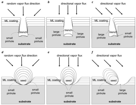
Figure 23.
Schematic illustration of pinhole defect formation in thin films under different vapor flux conditions, depicting how random and directional deposition influence pit evolution, size, and surface morphology (a) random vapor flux over a narrow, deep trench producing small pinholes; (b) directional vapor flux over a shallow trench resulting in larger pinholes due to stronger shadowing; (c) directional vapor flux over a wide trench leading to pronounced pinhole formation; (d) random vapor flux around a surface seed defect generating small pinholes; (e) directional vapor flux on a surface seed causing small pinholes to elongate along the flux direction; (f) directional vapor flux on a seed defect producing a large pinhole due to enhanced shadowing effects [133].
The directionality of vapor flux is a crucial factor influencing pinhole morphology. Under random vapor flux, deposition occurs isotropically, and small pinholes tend to close as the film thickens. Conversely, directional vapor flux—typical in sputtering or evaporation processes with restricted angular distribution—leads to columnar growth and shadowing, resulting in the formation of larger, persistent pinholes. These openings often arise from geometric shadowing at grain boundaries, foreign particle overgrowth, or insufficient ad-atom mobility during low-temperature deposition.
According to Panjan et al., pinholes can also nucleate from pits or inclusions on the substrate or by coalescence of gaps between neighboring columnar grains. Once formed, they significantly degrade the barrier, dielectric, and corrosion-resistance properties of the coating by acting as diffusion channels for oxygen, moisture, or reactive species. Their occurrence is particularly detrimental in protective and electronic films, where high film density and surface integrity are essential. Therefore, optimizing deposition parameters such as substrate temperature, plasma density, and incident flux angle, alongside post-deposition sealing or annealing, is vital for minimizing pinhole density and enhancing film reliability [133].
In reality, these defect categories seldom appear alone; instead, they frequently interact and develop as time passes. For example, vacancies may move and group together to create voids, while dislocations can offer favored diffusion pathways that enhance void expansion. The existence of pinholes can worsen corrosion or oxidation, leading to the formation of additional defects. Consequently, the reliability of thin films is closely linked to managing the initial defect population during manufacturing and the following defect progression during operation.
In terms of stability, thin films with a high defect concentration generally show more rapid deterioration when subjected to thermal, mechanical, and environmental stressors. In organic–inorganic hybrid films, pinholes may facilitate moisture entry, leading to swift chemical breakdown. In semiconductor films, dislocations may serve as starting points for stress-induced fractures during thermal cycles. Consequently, defect characterization—employing methods like AFM [472], scanning electron microscopy (SEM) [473], transmission electron microscopy (TEM) [474], and spectroscopic techniques—is a crucial stage in quality assurance and lifetime forecasting [472].
As depicted in Figure 24, Wu et al. investigated the nanoscale topography and surface potential of Ag–PCPDTBT hybrid films using AFM and Scanning Kelvin Probe Microscopy (SKPM) to elucidate their light-induced charge dynamics. The AFM image (Figure 24a) confirms a uniform distribution of Ag nanoparticles with an average particle size of approximately 120 nm, forming a continuous and well-connected nanostructured layer atop the conductive polymer matrix. The SKPM potential map under dark conditions (Figure 24b) reveals a higher surface potential at the Ag NP sites relative to the polymer regions, indicative of electron-rich zones associated with metallic Ag. Upon illumination with a 488 nm laser (Figure 24c), a significant decrease in potential is observed over the Ag domains—appearing as darker regions—corresponding to photoexcited electron transfer from the PCPDTBT polymer to the Ag nanoparticles. The height profile (Figure 24d) provides quantitative topographic evidence of the nanoparticle distribution, with a measured vertical height of ~120 nm consistent with AFM analysis. Meanwhile, the light-modulated surface potential plot (Figure 24e) captures the reversible changes in potential between the Ag and polymer phases under alternating light on/off cycles, confirming the formation of a transient photoinduced dipole layer at the Ag–PCPDTBT interface [475].
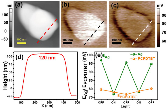
Figure 24.
Atomic force microscopy (AFM) and scanning Kelvin probe microscopy (SKPM) characterization of Ag nanoparticles on PCPDTBT films showing topography, surface potential under light/dark conditions, height profile, and light-modulated potential response (a) AFM topography of Ag nanoparticles on the PCPDTBT film; (b) SKPM surface potential image under dark conditions; (c) SKPM surface potential image under 488 nm light illumination; (d) height profile of the Ag nanoparticle showing ~120 nm height; (e) light-modulated surface potential response of Ag and PCPDTBT under alternating light ON/OFF conditions [475].
This reversible surface potential modulation highlights the plasmon-enhanced charge separation mechanism facilitated by the localized surface plasmon resonance (LSPR) of Ag nanoparticles, enhancing interfacial electron transfer efficiency within the hybrid film system.
In conclusion, vacancies, dislocations, voids, and pinholes are essential defect types that influence the functional reliability and durability of thin films. Successful defect management necessitates a blend of meticulous substrate preparation, refined deposition parameters, post-growth processes, and protective strategies during use. The difficulty is in harmonizing affordable production with strict defect management, making certain that thin films fulfill the high-performance standards of contemporary technologies.
7.2. Mitigation: Passivation, Encapsulation, Multilayer Barriers
The durability and stability of thin films over time are significantly affected by their capacity to withstand environmental and operational deterioration. Films with great initial qualities may still experience moisture intrusion, oxidation, UV degradation, thermal stress, and chemical damage if they are not adequately safeguarded. As a result, mitigation strategies are essential in thin film engineering, focused on reducing or preventing the emergence of defects, deterioration, and mechanical breakdown. Some of the most efficient methods include passivation, encapsulation, and multilayer barrier designs, each aimed at particular failure routes while frequently enhancing each other [476].
Passivation [477] entails using a protective coating or chemical treatment that makes the surface less sensitive to environmental factors like oxygen, moisture, or corrosive substances. In inorganic thin films, passivation layers typically comprise stable, dense oxides, nitrides, or carbides applied through methods like ALD or plasma-enhanced chemical vapor deposition (PECVD) [478]. An ultrathin layer of Al2O3 or Si3N4 can efficiently prevent oxygen diffusion and diminish surface oxidation in metallic or semiconductor films. In organic or hybrid thin films, passivation can include utilizing hydrophobic coatings, self-assembled monolayers, or chemical alterations that render reactive sites inactive. In addition to inhibiting corrosion and oxidation, passivation can also diminish surface recombination in optoelectronic devices, which enhances efficiency and prolongs operational lifespan [477].
Encapsulation [479] enhances protection by completely encasing the thin film or device inside a durable and chemically unreactive layer. This method is prevalent in areas like OLEDs, perovskite solar cells, and flexible electronics, where exposure to the environment may lead to quick deterioration. Encapsulation materials can be either rigid (such as glass or metal foil) or flexible (like polymer laminates and barrier-coated films), based on the device’s form factor. Stiff encapsulation provides outstanding barrier capabilities but restricts flexibility, while pliable encapsulation allows for bendable devices at the cost of marginally diminished protection. Techniques for depositing encapsulation layers consist of lamination, sputtering, evaporation, and roll-to-roll coating. In numerous situations, encapsulation also offers mechanical support, safeguarding against abrasion, impact, and handling harm [479].
Multilayer barriers [480] incorporate various materials in successive layers to improve defense by creating a complex diffusion route. This design significantly increases the difficulty for moisture, oxygen, or other damaging substances to infiltrate the film. Generally, inorganic films like oxides or nitrides are interspersed with organic or polymer films to merge the impermeability of inorganics with the flexibility and defect-repair capability of organics. The organic layers can separate cracks and imperfections in the inorganic layers, stopping them from forming continuous paths for diffusion [481]. This design is especially beneficial in flexible electronics, food packaging, and medical coatings, where mechanical flexibility and excellent barrier performance are needed. Multilayer barriers can be produced by sequential vacuum deposition, layer-by-layer self-assembly, or a combination of solution and vapor processing [480].
In reality, these mitigation strategies are frequently implemented together. A passivation layer can be directly applied to the functional thin film, succeeded by a multilayer barrier stack, and ultimately enclosed in a protective housing. The combination of these techniques relies on the particular performance needs, budget limitations, and device design.
The efficiency of passivation, encapsulation, and multilayer barriers is usually assessed through accelerated aging tests like damp heat exposure, UV–humidity cycling, and salt spray testing. These evaluations replicate actual operating conditions and enable forecasting of service life spans. Sophisticated characterization methods such as ToF-SIMS and cross-sectional electron microscopy are employed to assess barrier integrity and identify early-stage failures.
In general, mitigation strategies are fundamental components of thin film design and production rather than mere afterthoughts. Through the use of strong passivation, long-lasting encapsulation, and meticulously designed multilayer barriers, the reliability and stability of thin films can be significantly improved, allowing them to fulfill the requirements of high-performance applications in electronics, energy, optics, biomedical devices, and protective coatings.
Table 5 summarizes the principal failure mechanisms encountered in thin film systems, linking their physical origins to standardized test protocols and mitigation strategies. These degradation pathways define the long-term reliability and functional stability of coatings used in electronics, optics, and energy devices. The table reveals that failure is rarely caused by a single factor; rather, it emerges from the interaction between mechanical stress, thermal load, environmental exposure, and electrical bias.
Table 5.
Failure modes, testing protocols, and mitigation strategies in thin films.
Adhesion loss and cracking dominate mechanically driven failures, especially where residual stress and coefficient of thermal expansion mismatch lead to delamination during thermal cycling or bending. Electrical breakdown, ion migration, and electromigration illustrate field-driven degradation in dielectrics, perovskites, and metallic interconnects, respectively. Corrosion, oxidation, and moisture ingress remain pervasive in outdoor and flexible devices, particularly when barrier layers are thin or poorly sealed. Thermal and radiation-induced damage highlight the need for compositionally stable, defect-tolerant materials. Collectively, these examples emphasize that microstructural control, stress management, and robust encapsulation are the cornerstones of reliability engineering in thin films.
The mapping in Table 5 integrates laboratory testing with design solutions: American Society for Testing and Materials (ASTM) and Joint Electron Device Engineering Council (JEDEC) standards provide quantifiable reliability metrics, while mitigation approaches—graded interfaces, dopant stabilization, diffusion barriers, and hybrid encapsulation—translate scientific understanding into practical durability. Viewing these relationships together enables predictive reliability modeling and guides the selection of materials and processes for harsh environment applications.
In summary, Table 5 highlights the interconnected nature of thin film degradation, showing that mechanical, thermal, chemical, and electrical stresses often act concurrently. No single mitigation strategy guarantees reliability across all regimes; success depends on tailoring film composition, interface design, and encapsulation to the specific operating environment. As device architectures become thinner and more flexible, integrating reliability testing early in process development—using standardized adhesion, fatigue, and environmental protocols—becomes essential. The table, therefore, serves not only as a catalog of failure modes but also as a framework for designing resilient thin film systems that balance performance, durability, and manufacturability.
8. Computational Modeling and AI in Thin Films
8.1. Traditional: DFT, MD for Band Structure, Defect Energies, Stress Analysis
Computational modeling has historically been essential in grasping the basic properties of thin films, especially prior to extensive experimental synthesis. Conventional simulation methods like density functional theory (DFT) and molecular dynamics (MD) have been extensively utilized to investigate their electronic, structural, and mechanical characteristics. These techniques offer insights at the atomic level, allowing researchers to anticipate material behavior, investigate defect impacts, and refine deposition conditions [495].
DFT has established itself as the conventional quantum mechanical method for forecasting the band structure of thin films. Through the resolution of the electronic structure issue with clear approximations, DFT provides precise calculations of energy band gaps, effective masses, and trends in charge carrier mobility. This is especially crucial for semiconducting and optoelectronic thin films, as band alignment and defect states significantly impact device efficiency [496]. In photovoltaic absorber layers, DFT calculations can determine optimal doping methods, forecast interface states, and recommend compositional adjustments to enhance optical absorption. Additionally, DFT facilitates a thorough assessment of defect formation energies, making it possible to forecast which defects may occur under particular growth conditions and their effects on electrical or optical properties [497].
Molecular dynamics, however, is a classical simulation method that monitors the time progression of atomic systems according to interatomic potentials. MD is particularly useful for investigating dynamic phenomena like film formation, interface development, grain boundary movement, and thermal stability. It can record atomic diffusion during deposition, stress build-up from lattice mismatch, and crack formation under thermal cycling [498]. Using MD simulations, scientists can evaluate how process parameters like substrate temperature, deposition rate, and ambient gas composition influence microstructural evolution. This ability is essential for substances such as metal and ceramic coatings, where mechanical performance relies significantly on the states of residual stress and the distributions of defects [499].
Conventional computational techniques also offer stress analysis at the nanoscale, which is crucial for forecasting the longevity of thin films. DFT can assess intrinsic stress factors due to electronic influences, whereas MD can model the changes in mechanical stress during operational cycles or environmental conditions. Integrating both methods provides a fuller understanding, as DFT delivers high precision for small systems while MD allows for the investigation of larger, more realistic structures over extended timescales.
A key advantage of these conventional techniques is their ability to predict outcomes before manufacturing. By examining the relationship between band structure, defect energetics, and stress development, researchers can choose material compositions and deposition methods that are more likely to produce stable, high-performance films. Nonetheless, these techniques come with inherent compromises: DFT can be resource-heavy for sizable systems, and the accuracy of MD is heavily contingent on the quality of the interatomic potential employed.
In spite of these obstacles, DFT and MD continue to be essential tools in thin film studies. They are frequently utilized alongside experimental studies, where simulation outcomes assist in understanding characterization data from methods such as X-ray diffraction, electron microscopy, or Raman spectroscopy. This collaboration between theory and experimentation allows for a more effective design–build–test process, minimizing expensive trial-and-error in the lab. With the growth of thin film applications in flexible electronics, energy harvesting, and advanced protective coatings, traditional modeling methods will remain essential, while also incorporating newer AI-driven predictive frameworks to enhance discovery.
8.2. Machine Learning: Predicting Bandgaps, Conductivity, Adhesion
The use of machine learning (ML) in thin film research has become a groundbreaking method, allowing quick property forecasting and material discovery that surpasses conventional computational techniques. Although traditional methods such as DFT and MD offer accurate insights, they require significant computational resources, particularly when examining extensive compositional or structural domains [500]. ML models, developed using selected datasets from experiments or simulations, can swiftly and efficiently forecast essential thin film characteristics like bandgap, electrical conductivity, and adhesion strength [501].
Estimating the bandgap of thin films is crucial for uses in photovoltaics, photodetectors, and transparent electronic devices. Machine learning models can utilize datasets with chemical compositions, crystallographic parameters, and structural descriptors to quickly predict bandgap values for new materials. Methods like random forests, gradient boosting, and neural networks have shown capacity to identify intricate, non-linear associations between composition and electronic attributes. This feature enables researchers to effectively evaluate thousands of candidate materials and concentrate solely on the most promising options for experimental synthesis [502].
Likewise, ML is demonstrating great efficiency in predicting electrical conductivity, a characteristic affected by several interconnected factors like carrier concentration, mobility, grain boundary scattering, and defect density. Through the use of high-throughput simulation data or experimental measurements, ML models can identify relationships between processing parameters—such as deposition temperature, doping concentration, and annealing conditions—and the resulting conductivity values [503]. These predictive models not only speed up material optimization, but also assist in discovering unconventional compositions or nanostructures that could demonstrate enhanced performance [504].
Besides electronic properties, ML is being increasingly utilized to assess adhesion strength between thin films and their substrates. Adhesion is essential for establishing the mechanical stability and longevity of coatings, especially in high-stress fields like aerospace, biomedical implants, and MEMS. Integrating descriptors associated with surface energy, lattice mismatch, and interfacial chemistry, machine learning models can swiftly evaluate film–substrate compatibility. This method lessens dependence on extensive experimental adhesion testing, which can be both time-consuming and resource-heavy.
A key benefit of ML in thin film studies is its capability to merge multi-source datasets—integrating experimental data, simulation results, and published values—to create strong predictive models. Data preprocessing, feature engineering, and dimensionality reduction methods enhance input variables, ensuring models identify the most significant physical relationships. Additionally, active learning techniques enable ML algorithms to continuously propose the next most informative experiments or simulations, thus enhancing the data collection process.
Nevertheless, the effectiveness of ML models is highly reliant on the quality, diversity, and representation of data. Inadequately assembled datasets or limited sampling of the compositional space may result in erroneous predictions. To tackle this issue, researchers are progressively integrating ML with physics-based limitations, guaranteeing that predictions stay physically plausible. This physics-informed ML method connects purely data-driven models with established theoretical principles, offering greater confidence in predictions for unexamined materials.
As applications of thin films expand into energy harvesting, flexible electronics, high-barrier coatings, and quantum devices, the capacity to swiftly predict and enhance properties will be crucial. ML provides a route to expedited discovery by facilitating virtual prototyping, uncovering property–structure–process connections, and directing focused experiments. When combined with conventional computational techniques and experimental feedback loops, ML can considerably reduce the development timeline for high-performance thin films and broaden the search range to material systems that were previously out of reach.
8.3. High-Throughput Screening: Databases (Materials Project, AFLOW)
High-throughput screening (HTS) has emerged as a crucial method in thin film research, facilitating swift assessment of material candidates over extensive compositional and structural ranges. HTS utilizes computational tools, automated workflows, and extensive materials databases to predict and filter properties before synthesis, rather than depending only on slow, sequential experimental trials. This approach significantly speeds up the identification of thin films with specific electronic, optical, or mechanical properties, while also lowering the expenses and duration linked to conventional development processes [505].
The basis of HTS in materials science resides in combined computational materials databases like the Materials Project and AFLOW (Automatic Flow for Materials Discovery). These platforms retain pre-calculated material characteristics acquired from DFT and various quantum mechanical simulations. These databases offer essential data for thin films, including crystal structure, bandgap, elastic constants, surface energies, and thermodynamic stability. Researchers can interrogate these datasets to find materials that satisfy certain requirements, like ideal band alignment for solar cells, elevated dielectric constant for capacitors, or minimal lattice mismatch for epitaxial growth [506].
The Materials Project provides a vast database of more than 150,000 inorganic materials, featuring searchable property information and crystal structures that can be accessed through an easy-to-use interface and API. For thin film uses, the platform enables focused searches for appropriate substrates, interlayers, and functional layers by applying filters according to symmetry, bandgap, and stability metrics. The AFLOW database enhances this by offering a highly automated system for creating datasets of material properties, such as electronic band structures, phonon dispersions, and mechanical moduli. By concentrating on automation, it allows for the consistent evaluation of numerous materials, establishing it as an effective resource for selecting candidates for coating, optical, and semiconductor thin films [507].
High-throughput methods also go beyond simple property acquisition. By combining database data with workflow automation tools, researchers can conduct virtual experiments that replicate actual deposition situations. For instance, HTS can recognize materials with suitable surface terminations for heterostructure development, forecast the stability of ultrathin layers when under strain, or assess the influence of doping on conductivity and adhesion. HTS platforms can, when used with machine learning models, not only access existing data but also estimate and forecast properties for unexamined materials, thereby broadening the searchable area without incurring further costly simulations [508].
A significant function of HTS is its involvement in multi-objective optimization. Thin film design frequently requires balancing trade-offs, like enhancing conductivity while ensuring mechanical stability, or attaining a low refractive index without sacrificing thermal resilience. Utilizing database-driven screening, researchers can efficiently prioritize candidate materials according to various performance metrics and choose the optimal compromises for testing.
Even with its benefits, HTS is constrained by the precision of the foundational data and the applicability of the computational models employed. Numerous properties of thin films, including adhesion strength, tolerance to defects, and stability in real-world environments, are difficult to accurately assess at large scales. Consequently, HTS works best when implemented as an initial screening phase, succeeded by focused experimental confirmation. This combined method guarantees that computational forecasts stay rooted in realistic applicability.
8.4. Autonomous Labs: Bayesian Optimization + Robotics for Closed-Loop Synthesis
The idea of autonomous laboratories is revolutionizing thin film research by uniting Artificial Intelligence (AI), sophisticated optimization algorithms, and robotic synthesis systems into a comprehensive, closed-loop discovery system. These systems are capable of designing, conducting, and optimizing experiments with little human involvement, facilitating quick examination of intricate processes–property correlations that would be challenging to explore by hand. In the realm of thin films, self-operating laboratories greatly speed up the fine-tuning of deposition settings, material formulations, and post-treatment conditions.
A key aspect of this method is Bayesian optimization (BO), a statistical technique that effectively explores vast parameter spaces while reducing the number of necessary experiments. In contrast to brute-force screening, Bayesian optimization employs a surrogate model—typically a Gaussian process—to anticipate material performance in untested conditions and to direct the choice of the next most promising experiment [509]. This is especially useful for thin film synthesis, where factors like substrate temperature, deposition rate, gas flow composition, and annealing time interact in complex ways to affect properties such as bandgap, conductivity, and adhesion [509].
Robotics serves as the physical foundation of self-sufficient laboratories. Automated deposition systems—like robotic sputtering machines, inkjet printers, and CVD systems—can perform accurate, consistent synthesis procedures based on directives produced by the optimization algorithm [510]. Integrated in situ and ex situ characterization methods, including spectroscopic ellipsometry, X-ray diffraction, or four-point probe techniques, provide property data for the optimization loop. This establishes a closed-loop system in which synthesis, measurement, and decision-making happen perpetually without human involvement [510].
The strength of these systems is found in their capacity to continuously enhance experiments instantly. An autonomous thin film laboratory could start with diverse deposition conditions, rapidly pinpoint areas of the parameter space that produce high-quality films, and subsequently concentrate on optimizing those conditions. Bayesian optimization guarantees that every new experiment maximizes the information acquired, minimizing the total iterations required to find an optimal solution [511].
This approach is particularly useful for multi-objective optimization, frequently encountered in thin film engineering. Applications like transparent conductors, protective coatings, and photovoltaic absorbers frequently necessitate a delicate equilibrium of conflicting characteristics—high conductivity while maintaining optical clarity, or mechanical strength without significantly increasing thickness. Autonomous systems can handle these trade-offs more effectively than manual testing by evaluating various performance metrics at the same time [512].
Besides speeding up discovery, autonomous labs provide advantages in reproducibility and scalability. Utilizing robotics removes inconsistencies caused by manual handling, guaranteeing that outcomes remain uniform across experiments and labs. After an ideal synthesis procedure is established, it can be directly scaled or adapted for production settings with little alteration. Additionally, the data-rich characteristics of these platforms enable the development of extensive synthesis–property databases that can support future machine learning models, improving predictive abilities for new material systems [513].
Nonetheless, some obstacles need to be tackled. The effectiveness of Bayesian optimization relies on the quality and comprehensiveness of the initial dataset, and robotic systems need to be adequately flexible to accommodate various thin film materials and deposition techniques. Incorporating real-time feedback from sophisticated characterization tools necessitates precise coordination between software and hardware elements. In spite of these challenges, autonomous laboratories signify a major change in self-driving materials discovery, enabling the synergy of AI and robotics to reduce development times from years to months or even weeks.
As the field develops, it is probable that autonomous laboratories for thin films will more often function in distributed networks, exchanging data and synthesis methods worldwide. These systems will enhance the optimization of existing materials and facilitate the swift identification of completely new thin film compositions and structures designed for advanced electronic, optical, and protective applications.
As illustrated in Figure 25, Ma et al. proposed a comprehensive machine learning framework for the inverse design of optical multilayer thin films, integrating multiple encoding strategies to optimize both material selection and layer geometry. The schematic in Figure 25A presents a five-layer thin film stack comprising alternating materials with adjustable layer thicknesses—serving as the design space for optical property optimization. In Figure 25B, the vectorized representation treats layer thicknesses as continuous variables while keeping material types fixed, effectively transforming the thin film design problem into a multidimensional numerical optimization task. This approach is computationally efficient and well-suited for cases where the constituent materials are predetermined but optimal thickness profiles are unknown. In contrast, Figure 25C illustrates the combined representation, where both the material identity and layer thickness are optimized simultaneously. This method allows for the automated discovery of new multilayer architectures that achieve target optical responses—such as reflectance spectra, photonic band gaps, or specific color coordinates—through high-dimensional co-optimization. Finally, Figure 25D depicts the sequential representation, a hierarchical design approach where the machine learning model predicts each layer iteratively, co-optimizing the material and thickness in a stepwise fashion. This sequential encoding closely emulates the physical deposition sequence in practical thin film fabrication and improves generalizability by capturing interlayer dependencies [514].
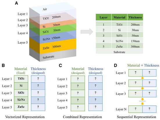
Figure 25.
Machine learning (ML) framework for multilayer thin film optimization. (A) Five-layer structure schematic with layer-specific materials and thicknesses. (B) Vectorized representation—materials are fixed while thicknesses are optimized. (C) Combined representation—both material type and thickness are treated as design variables. (D) Sequential representation—layer material and thickness are co-optimized in a stepwise, layer-by-layer approach [514].
Together, these representations form a robust foundation for AI-driven inverse design and autonomous synthesis, bridging the gap between data-driven prediction and experimental realization. This framework not only accelerates multilayer optical coating development but also serves as a key paradigm for closed-loop, self-optimizing laboratories, where Bayesian optimization and robotics govern thin film synthesis and characterization.
9. Critical Gaps, Challenges, and Future
9.1. Scientific Challenges-Stability, Defect Control, 2D Heterostructures
Stability—fundamental materials and device-level limits: The long-term operational stability of atomically thin sensing films is governed by a combination of intrinsic thermodynamic driving forces and extrinsic environmental stressors, where oxygen, moisture, light, and ion migration produce structural and chemical transformations that alter electronic and ionic transport pathways [515]. The ultra-high surface-to-volume ratio of 2D crystals that gives them excellent sensitivity simultaneously renders them kinetically prone to surface adsorption, oxidation and etching processes that create time-dependent variability in baseline and responsivity for sensing applications [516]. Interfacial instability—arising from weak van der Waals contacts, trapped adsorbates, and poorly matched work functions between films and electrodes—induces contact resistance drift, hysteresis, and bias-stress degradation under electrical operation in real-world environments [517]. Mitigation strategies that have demonstrated partial success combine encapsulation using chemically inert 2D barriers or polymer overlayers, compositional engineering to reduce volatile species and ion migration, and process controls that minimize defect densities; however, these approaches often trade off sensitivity, fabrication complexity, or device scalability and therefore do not yet constitute a general solution for field-deployed sensors [516].
Defect control—opportunities and precision engineering: Native and process-induced point defects, line defects and grain boundaries fundamentally define carrier scattering, trap states, catalytic activity and chemical reactivity in 2D sensing films, and therefore act as both performance levers and reliability hazards [518]. At the atomic scale, chalcogen vacancies in transition-metal dichalcogenides and iodine vacancies in halide perovskites are dominant non-radiative recombination and trap centers that reduce signal-to-noise and accelerate material degradation, while controlled introduction of substitutional dopants or vacancy complexes can be used intentionally to tune carrier density and adsorption energetics for enhanced selectivity [516,518]. Current defect engineering toolsets—ion irradiation, electron beam patterning, plasma functionalization, seeded growth and chemical passivation—offer sub-nm to nm-scale control but suffer from throughput, collateral damage and poor process window definition, so translating lab-scale defect patterning into wafer-scale, reproducible production remains an open engineering challenge [516]. Advanced in situ metrology (operando TEM, synchrotron XPS, and scanning probe spectroscopy) combined with data-driven inverse design is emerging as a promising pathway to correlate atomic defect fingerprints with macroscopic device metrics and thereby shorten the optimization loop for stable, high-yield sensor films.
2D heterostructures—integration, interlayer physics, and scaling: van der Waals heterostructures enable designer band alignments, interlayer charge transfer and engineered excitonic states that can dramatically expand sensing modalities, yet heterointerface cleanliness, twist angle control and strain management are decisive factors that govern interlayer coupling and device reproducibility [517]. Fabrication strategies—mechanical stacking, deterministic transfer, and direct heteroepitaxy—each present different tradeoffs between interface contamination, throughput and lattice matching, and uncontrolled residues or trapped adsorbates at the interface can introduce mid-gap states that dominate low-frequency noise and drift in sensors. From a systems perspective, assembling multifunctional heterostructures into device stacks while maintaining process compatibility with encapsulation, interconnects and readout electronics requires co-optimization of thermal budgets, chemical exposure and mechanical handling to avoid creating new pathways for degradation. Looking forward, deterministic control of interlayer registry and engineered interface chemistries enabled by layer-by-layer automated growth and scalable transfer protocols, paired with machine-assisted metrology to detect subtle interfacial defects, will be central to moving 2D heterostructure sensors from proof-of-concept to robust deployed platforms.
9.2. Technical Gaps
At the process level, scaling two-dimensional (2D) sensing films from demonstrations to wafer-scale manufacturing is fundamentally constrained by stochastic nucleation and lateral coalescence during vapor-phase syntheses, which generate polycrystalline films with grain boundaries and thickness non-uniformities that map directly to device-to-device variability and yield loss [519]. The literature identifies three principal growth strategies to address misorientation and stitching—isolated-domain growth with single nucleation events, unidirectional domain alignment, and conversion of oriented precursors—but implementing any of these approaches uniformly across 150–300 mm wafers used in semiconductor fabs remains challenging because of reactor scale-up, precursor flux control, and substrate conditioning requirements [520]. Even where low-thermal-budget reactors and precursor-separation geometries enable direct monolayer TMD growth on 200 mm BEOL-compatible platforms, the reported electrical uniformity metrics (for example, MoS2 mobilities on the order of 30–40 cm2 V−1 s−1) are highly sensitive to local nucleation density, precursor partial-pressure gradients, and residual particulates, which require closed-loop reactor control and wafer-level process maps to approach fab tolerances [521]. In practice, transfer-based toolchains (wet chemical release, polymer support delamination, or template stripping) that remain common in research settings systematically introduce residues, wrinkles, and mechanical strain that degrade baseline noise, contact resistance, and long-term drift in sensor arrays; therefore creating an unresolved throughput–cleanliness tradeoff for high-volume manufacture [520]. Consequently, unless deterministic nucleation control, in situ stitching methods, or robust transfer-free epitaxy are scaled and validated at wafer-fab dimensions, 2D sensing films will be confined to low-volume or niche sensor nodes rather than embedded CMOS sensor platforms at industrial volumes [519].
Integration with silicon CMOS imposes coupled materials and process constraints that go beyond mere film deposition: first, back-end-of-line (BEOL) thermal budgets (typically <400 °C and often constrained to <300 °C for advanced nodes) preclude many conventional high-temperature CVD recipes and therefore motivate low-temperature syntheses, remote precursor decomposition, and transfer strategies that require the control of contamination and residuals [521]. Second, forming a gate dielectric with an equivalent oxide thickness (EOT) approaching 1 nm while avoiding interface traps is fundamentally difficult because ALD nucleation does not proceed readily on pristine van der Waals surfaces without seeding or controlled functionalization, and every seeding strategy brings trade-offs in fixed charge, trap density and process compatibility with CMOS gate stacks [522]. Third, contact engineering is the single most acute device-level integration challenge: although edge and semi-metal contacts and regrown contact regions have reduced contact resistance in laboratory devices, producing reproducible, low-variability, low-resistivity contacts at the sub-20 nm contact lengths required for scaled nodes has not been demonstrated at wafer scale and is sensitive to thermal processes, metal interdiffusion and process-induced damage; alternative approaches such as transferred prefabricated metal electrodes or quasi-van der Waals epitaxy are promising but need demonstration under fab contamination rules [522]. Finally, successful integration requires not only device-level recipes but full foundry-grade process flows—planarization and via formation compatible with multilayer interconnects, contamination and particle budgets, and standardized reliability test structures—because sensor arrays must meet the same yield, variability and lifetime expectations as other CMOS elements for system-level adoption [516].
Environmental durability presents a multi-physics failure surface that is especially severe for atomically thin sensors: monolayer and few-layer films expose every active atom to ambient moisture, oxygen, and chemically active analytes, enabling chemisorption, oxidative transformation, and intercalation processes that alter baseline carrier density, mobility, and sensor selectivity [523]. Aging studies of CVD TMDs (for example, MoS2) document oxidative conversion and the growth of Mo-oxide species and dendritic nanostructures over months under typical ambient humidity, which manifests as baseline drift, increased noise, and eventual device failure if protective strategies are not implemented [523]. Encapsulation approaches—van der Waals capping with h-BN, conformal ALD oxide overlayers, polymer encapsulants, or hybrid multilayer barriers—can significantly extend operational life, but each approach imposes trade-offs: h-BN provides an atomically clean van der Waals (vdW) interface but can mechanically strain or alter phonon/exciton properties; ALD provides conformal hermeticity but can introduce charge traps and requires nucleation engineering; polymers are scalable but provide inferior gas/water impermeability relative to inorganic barriers [524]. For nanofluidic and nanopore devices, modifying the supporting substrate chemistry and reducing oxidative species in the operating solution have demonstrably improved nanopore lifetime and measurement stability, but these methods must be reconciled with manufacturability and analyte accessibility requirements for deployed chemical sensors in food matrices [525]. Therefore, pragmatic durability engineering for food-quality monitoring will require material selection (favoring less reactive 2D chemistries for the given analyte), multilayer encapsulation stacks with quantified barrier transmission rates, and architectural choices that enable periodic in situ calibration or replaceable sensing elements to meet both sensitivity and longevity targets [526].
Bridging these gaps leads to a concrete, engineering-centered roadmap: (a) process engineering must deliver deterministic nucleation control and wafer-scale single-crystal or unidirectionally stitched films via reactor redesign and precursor engineering, accompanied by wafer-level metrology (automated Raman/PL maps, wafer reflectometry, in situ optical monitoring) to drive closed-loop control [520]. (b) Integration modules must be modularized into foundry-acceptable unit processes—low-temperature direct growth or a validated high-yield transfer protocol for 200–300 mm wafers, encapsulation blocks with ALD/VDW hybrid recipes, and standardized contact modules (transferred metal electrodes or ALD/edge contact hybrids)—each with contamination and particle budgets documented for integration into BEOL flow [521]. (c) Reliability and qualification require adoption of statistical device benchmarking, test structures and accelerated lifetime testing (Highly Accelerated Stress Test (HAST), temperature-humidity cycling, bias-temperature stress) together with published datasets on variability and failure modes so that circuit designers can build calibration and redundancy schemes into readout ASICs [516]. (d) Finally, ecosystem engineering—supply chains for high-purity precursors, patterning and metrology tool development, and open foundry–academic collaborations that provide standardized process recipes and reference wafers—will be as decisive as any single materials breakthrough in enabling CMOS-integrated 2D sensing at scale [519].
9.3. Future Vision: Eco-Friendly, AI-Driven, Reproducible Thin Film Science
The future of thin film science will focus on a solid commitment to environmental sustainability, data-oriented innovation, and reproducible research methods. As thin films increase their significance in energy, electronics, healthcare, and environmental systems, attention is moving from solely performance-based development to strategies that also consider ecological effects, ethical manufacturing, and lasting reliability. This transition is being hastened by worldwide climate objectives, the rising accessibility of sophisticated computational resources, and heightened requests for transparency in scientific processes.
The advancement of eco-friendly thin films is anticipated to be crucial in minimizing the environmental impact of production. This entails embracing green chemistry principles, utilizing non-toxic and plentiful raw materials, and reducing the reliance on hazardous solvents and energy-intensive, high-vacuum processes. Alternative deposition methods like solution processing, low-temperature CVD, and bio-inspired fabrication are becoming popular due to their lower energy needs and compatibility with biodegradable materials [527]. Circular design ideas, featuring thin films engineered for easy disassembly and recycling, will gain prevalence in consumer electronics, solar panels, and intelligent packaging. Lifecycle assessment tools will direct material and process selections, making sure that environmental benefits are measured and maximized throughout the supply chain [527].
Research on thin films powered by AI is becoming a groundbreaking method for speeding up material discovery, enhancing process parameters, and forecasting long-term device efficiency. Machine learning models are capable of examining large datasets derived from experiments and simulations to determine ideal compositions, deposition parameters, and post-processing methods. Autonomous laboratories with closed loops are starting to combine AI and robotics, facilitating ongoing, self-optimizing processes for synthesis and characterization [528]. Digital replicas of deposition systems enable real-time process management and defect forecasting, greatly minimizing trial-and-error cycles. Moreover, AI-based image analysis and sensor integration are enhancing in situ monitoring, guaranteeing uniform quality in extensive manufacturing processes [528].
Reproducibility in thin film science is becoming more important as research complexity rises and materials are utilized in commercial applications. Inconsistent reporting in experiments and variation in measurement methods can obstruct technology transfer and widespread adoption. To tackle this, standardized characterization protocols, open access data archives, and comprehensive metadata regarding experimental conditions are increasingly crucial. Automation and digital documentation minimize human mistakes, whereas consistent computational procedures guarantee that simulations can be verified and contrasted among various research teams. This culture of transparency not only enhances scientific trustworthiness but also accelerates cooperative innovation among academia, industry, and regulatory organizations [529].
The combination of these three elements—environmental sustainability, AI-enhanced optimization, and repeatability—will establish a thin film research and production system that is sustainable, effective, and internationally compatible. Materials will be conceived with environmental and ethical factors in mind from the beginning, enhanced via smart algorithms, and verified through clear, standardized processes [530].
In summary, the future perspective for thin films involves a transition towards smart, sustainable, and reproducible science that aligns performance with environmental stewardship and data reliability. This method will guarantee that thin film technologies stay leading in global innovation, while also aligning with societal and environmental concerns. While these challenges define the research frontier, recent quantitative gains in deposition control and device performance illustrate the tangible progress achieved to date.
10. Summary and Perspectives
The trajectory of thin film research tells a story of scientific curiosity steadily transformed into technological impact. What began with early experimental observations—simple trials to understand how materials behaved when reduced to ultrathin dimensions—evolved into systematic methods of deposition and characterization. Over time, researchers learned to manipulate atomic and molecular interactions, giving rise to controlled growth strategies that brought unprecedented precision in film quality and structural definition. This steady refinement shifted thin films from being valued primarily for their optical reflectivity or protective coatings into versatile building blocks of modern technology, powering innovations in microelectronics, sensors, energy harvesting devices, and biomedical applications.
The evolution of thin film science over the last three decades has transitioned from phenomenological exploration to quantitative, precision-controlled engineering. Deposition uniformity, atomic-level conformality, and defect minimization have become measurable standards rather than aspirational goals. For instance, ALD now achieves film-thickness deviations below ±1% over 300 mm wafers with angstrom-scale precision [172,175] and conformality ratios exceeding 95% for high-aspect-ratio trenches have been reported. Similarly, sputtering processes have achieved uniformity of ±2% on substrates up to 1 m2 in size [128,130]. These metrics signify an unprecedented reproducibility, making thin film fabrication ready for global industrial integration.
Quantitative progress is equally striking in performance metrics. Thin film photovoltaics, notably CdTe and CIGS, have crossed 22% power-conversion efficiency (PCE) [531] while perovskite thin films now report certified efficiencies > 26% [532]. Roll-to-roll printing and slot-die coating of perovskites have demonstrated large-area uniformity with 16–18% PCE on >200 cm2 modules [533]. Thin film transistors (TFTs) using amorphous In-Ga-Zn-O (a-IGZO) exhibit carrier mobilities of 10–20 cm2 V−1 s−1 and operational lifetimes exceeding 106 cycles [459]. These quantitative examples demonstrate the leap from laboratory thin film prototypes to reproducible, high-throughput industrial applications.
From a sustainability standpoint, modern fabrication strategies are rapidly incorporating LCA and green chemistry. Energy-efficient low-temperature ALD processes (<150 °C) reduce energy consumption by ~30% per batch compared to conventional thermal CVD [534]. Bio-inspired deposition and recyclable polymer substrates have been integrated into functional device platforms, decreasing carbon footprints while maintaining functional integrity [527]. Circular design and digital twins—using process data for closed-loop optimization—are emerging as central pillars for next-generation, climate-aligned thin film manufacturing [455].
Artificial intelligence (AI) and machine learning (ML) have transformed how thin film parameters are optimized and predicted. Inverse design frameworks have successfully optimized optical multilayers with >95% target accuracy using neural network-based architectures [514]. These AI-driven digital laboratories can predict growth rate deviations, defect densities, and even refractive index distributions in real time, reducing experimental iterations by nearly 40%. The next phase will involve federated data infrastructures that integrate distributed laboratories and enable meta-learning across materials, substrates, and deposition conditions—building toward an autonomous, globally networked materials discovery ecosystem.
Collectively, these developments affirm that thin film technologies have entered a mature yet continually expanding frontier where materials science, device engineering, and digital optimization converge. The field now stands at a transition point—from descriptive understanding to predictive, data-driven control—supported by quantitative validation and cross-disciplinary integration. As deposition precision, reliability, and sustainability advance in tandem, thin films are set to underpin the next generation of intelligent, energy-efficient, and miniaturized systems that define modern technology. The sustained dialog between experiment, computation, and industry will determine how swiftly these laboratory-level innovations translate into scalable, resilient, and environmentally responsible manufacturing paradigms. In essence, thin film science has evolved from the art of making coatings to the science of building futures.
Today, the field has matured into an interdisciplinary arena where material science, nanotechnology, and engineering converge. Thin films are no longer passive surface modifiers but active, multifunctional elements in next-generation systems. They now underpin flexible displays, wearable healthcare devices, high-efficiency solar cells, quantum computing architectures, and protective coatings designed for extreme environments. This transformation is enabled by a blend of traditional deposition techniques with emerging methods such as atomic layer precision, hybrid organic–inorganic architectures, and low-dimensional material integration. Coupled with in situ diagnostics and computational modeling, researchers can now anticipate film growth dynamics rather than relying solely on trial and error. Equally important is the ongoing shift from laboratory-scale prototypes toward industrial scalability, where reproducibility, uniformity, and reliability determine whether thin films successfully transition from experimental breakthroughs to globally adopted technologies.
Looking forward, three major themes are poised to define the future of thin film science. First is intelligent integration, where artificial intelligence, machine learning, and high-throughput experimentation are harnessed to accelerate material discovery and optimize process conditions in ways human intuition alone cannot achieve. Second is sustainable manufacturing, which will demand greener chemistries, recyclable substrates, low-energy deposition strategies, and closed-loop design principles that minimize waste while ensuring circularity of materials. Third is predictive and adaptive design, where autonomous, self-optimizing deposition platforms could tailor thin films dynamically in response to environmental conditions or application-specific requirements. These directions reflect a clear transition toward a research and manufacturing ecosystem that values not only performance, but also ecological responsibility and global accessibility.
The novelty of this review lies in weaving together this past–present–future narrative into a unified framework. By combining comparative tables, practical checklists, and a forward-looking roadmap, it does more than catalog advances—it creates a structured lens through which researchers and engineers can identify gaps, benchmark progress, and prioritize future directions. In doing so, it highlights the importance of integrating reproducibility, sustainability, and intelligent optimization as guiding principles for the next generation of thin film science. Ultimately, the path forward envisions a field where discovery and application progress hand in hand, ensuring that thin films remain at the forefront of technological revolutions while meeting the pressing societal demand for sustainable and reliable innovation.
Author Contributions
Conceptualization: A.P.A., J.H.P., R.K. and H.L.R.; Writing—original draft preparation: N.S. and A.P.A.; Formal analysis and investigation: N.S., R.K., J.H.P. and M.R.; Investigation and Resources: J.H.P., R.K. and H.L.R.; Conceptualization, Formal Analysis, Writing—review and editing: A.P.A. All authors have read and agreed to the published version of the manuscript.
Funding
This research received no external funding.
Data Availability Statement
No datasets were generated or analyzed during the current study.
Acknowledgments
The authors thank Principal, RV College of Engineering, and Rashtreeya Sikshana Samithi Trust (RSST) for their invaluable support and for providing the necessary facilities and encouragement throughout the course of this work.
Conflicts of Interest
Author Hemanth L. Ramachandraiah was employed by the company Samco Inc. The remaining authors declare that the research was conducted in the absence of any commercial or financial relationships that could be construed as a potential conflict of interest.
References
- Oviroh, P.O.; Akbarzadeh, R.; Pan, D.; Coetzee, R.A.M.; Jen, T.-C. New development of atomic layer deposition: Processes, methods and applications. Sci. Technol. Adv. Mater. 2019, 20, 465–496. [Google Scholar] [CrossRef]
- Barnasas, A.; Garoufalis, C.S.; Anyfantis, D.I.; Poulopoulos, P.; Baskoutas, S. On the Quantum Confinement Effects in Ultrathin PdO Films by Experiment and Theory. Materials 2022, 15, 8700. [Google Scholar] [CrossRef] [PubMed]
- Venables, J.A.; Spiller, G.D.T.; Hanbucken, M. Nucleation and growth of thin films. Rep. Prog. Phys. 1984, 47, 399. [Google Scholar] [CrossRef]
- Abadias, G.; Chason, E.; Keckes, J.; Sebastiani, M.; Thompson, G.B.; Barthel, E.; Doll, G.L.; Murray, C.E.; Stoessel, C.H.; Martinu, L. Review Article: Stress in thin films and coatings: Current status, challenges, and prospects. J. Vac. Sci. Technol. A 2018, 36, 020801. [Google Scholar] [CrossRef]
- El Messaoudi, N.; Franco, D.S.P.; Gubernat, S.; Georgin, J.; Şenol, Z.M.; Ciğeroğlu, Z.; Allouss, D.; El Hajam, M. Advances and future perspectives of water defluoridation by adsorption technology: A review. Environ. Res. 2024, 252, 118857. [Google Scholar] [CrossRef] [PubMed]
- Alessio, P.; da Silva, M.K.C.; Barossi, V.; Miyazaki, C.M. Nanostructured Thin Films Enhancing the Performance of New Organic Electronic Devices: Does It Make Sense? ACS Mater. Au 2024, 4, 574–581. [Google Scholar] [CrossRef]
- Aich, P.; Meneghini, C.; Tortora, L. Advances in Structural and Morphological Characterization of Thin Magnetic Films: A Review. Materials 2023, 16, 7331. [Google Scholar] [CrossRef]
- Văduva, M.; Baibarac, M.; Cramariuc, O. Functionalization of Graphene Derivatives with Conducting Polymers and Their Applications in Uric Acid Detection. Molecules 2022, 28, 135. [Google Scholar] [CrossRef] [PubMed]
- Shepelin, N.A.; Tehrani, Z.P.; Ohannessian, N.; Schneider, C.W.; Pergolesi, D.; Lippert, T. A practical guide to pulsed laser deposition. Chem. Soc. Rev. 2023, 52, 2294–2321. [Google Scholar] [CrossRef]
- Roeder, G.; Liu, S.; Aygun, G.; Evanschitzky, P.; Erdmann, A.; Schellenberger, M.; Pfitzner, L. Determination of the Dill parameters of thick positive resist for use in modeling applications. Thin Solid Film. 2011, 519, 2978–2984. [Google Scholar] [CrossRef][Green Version]
- Ukoba, K.; Jen, T.-C. Thin Films in Flexible Electronics. In Shaping Tomorrow: Thin Films and 3D Printing in the Fourth Industrial Revolution–Volume 2: Applications; Springer: Cham, Switzerland, 2025; pp. 1–75. [Google Scholar] [CrossRef]
- Ratsch, C.; Venables, J.A. Nucleation theory and the early stages of thin film growth. J. Vac. Sci. Technol. A 2003, 21, S96–S109. [Google Scholar] [CrossRef]
- Evans, J.W.; Thiel, P.A.; Bartelt, M.C. Morphological evolution during epitaxial thin film growth: Formation of 2D islands and 3D mounds. Surf. Sci. Rep. 2006, 61, 1–128. [Google Scholar] [CrossRef]
- Thanh, N.T.K.; Maclean, N.; Mahiddine, S. Mechanisms of Nucleation and Growth of Nanoparticles in Solution. Chem. Rev. 2014, 114, 7610–7630. [Google Scholar] [CrossRef]
- Nandy, A.; Duan, C.; Taylor, M.G.; Liu, F.; Steeves, A.H.; Kulik, H.J. Computational Discovery of Transition-metal Complexes: From High-throughput Screening to Machine Learning. Chem. Rev. 2021, 121, 9927–10000. [Google Scholar] [CrossRef]
- Ohring, M. Substrate Surfaces and Thin-Film Nucleation. In Materials Science of Thin Films, 2nd ed.; Academic Press: Cambridge, MA, USA, 2002; pp. 357–415. [Google Scholar] [CrossRef]
- Ruiz-Gómez, S.; Fernández-González, C.; Perez, L. Electrodeposition as a Tool for Nanostructuring Magnetic Materials. Micromachines 2022, 13, 1223. [Google Scholar] [CrossRef]
- Wang, T.; Li, Q.; Liu, X.; Bilal, M.; Dong, D.; Wang, H. Nanofabrication technologies for low-temperature solid oxide cells: A comprehensive review of techniques, challenges, and future perspectives. Energy Rev. 2025, 4, 100163. [Google Scholar] [CrossRef]
- Fornari, C.I.; Fornari, G.; Rappl, P.H.; Abramof, E.; Travelho, J.D.S. Monte Carlo Simulation of Epitaxial Growth. In Epitaxy; InTech: London, UK, 2018. [Google Scholar]
- Cranston, R.R.; Lessard, B.H. Metal phthalocyanines: Thin-film formation, microstructure, and physical properties. RSC Adv. 2021, 11, 21716–21737. [Google Scholar] [CrossRef] [PubMed]
- Abbas, M.; Zeng, L.; Guo, F.; Rauf, M.; Yuan, X.C.; Cai, B. A Critical Review on Crystal Growth Techniques for Scalable Deposition of Photovoltaic Perovskite Thin Films. Materials 2020, 13, 4851. [Google Scholar] [CrossRef]
- Kaiser, N. Review of the fundamentals of thin-film growth. Appl. Opt. 2002, 41, 3053–3060. [Google Scholar] [CrossRef]
- Prieto, J.E.; Markov, I. Stranski–Krastanov mechanism of growth and the effect of misfit sign on quantum dots nucleation. Surf. Sci. 2017, 664, 172–184. [Google Scholar] [CrossRef]
- Eisenberg, H.R.; Kandel, D. Origin and properties of the wetting layer and early evolution of epitaxially strained thin films. Phys. Rev. B 2002, 66, 155429. [Google Scholar] [CrossRef]
- Vasilakos, K.; Thomas, N.; Hermassi, M.; Campo, P.; McAdam, E. On the role of crystal-liquid interfacial energy in determining scaling, nucleation and crystal growth in membrane distillation crystallisation. J. Memb. Sci. 2025, 725, 123978. [Google Scholar] [CrossRef]
- Bera, S.; Das, S. Nucleation and particle growth in solution-processed thin films. In Chemical Solution Synthesis for Materials Design and Thin Film Device Applications; Elsevier: Amsterdam, The Netherlands, 2021; pp. 1–27. [Google Scholar] [CrossRef]
- Kalin, M.; Polajnar, M. The correlation between the surface energy, the contact angle and the spreading parameter, and their relevance for the wetting behaviour of DLC with lubricating oils. Tribol. Int. 2013, 66, 225–233. [Google Scholar] [CrossRef]
- Li, X.; Ren, L.; Zheng, X.; Poudel, B.; Wang, K.; Qian, J. Multiscale Coupling Between Macroscopic Mechanics and Atomic Assembly (MM–AA) of Soft-Lattice Halide Perovskites. Aggregate 2025, e70170. [Google Scholar] [CrossRef]
- Perez, M. Gibbs–Thomson effects in phase transformations. Scr. Mater. 2005, 52, 709–712. [Google Scholar] [CrossRef]
- McLean, J.G.; Krishnamachari, B.; Peale, D.R.; Chason, E.; Sethna, J.P.; Cooper, B.H. Decay of isolated surface features driven by the Gibbs-Thomson effect in an analytic model and a simulation. Phys. Rev. B 1997, 55, 1811–1823. [Google Scholar] [CrossRef]
- Krishnamachari, B.; McLean, J.; Cooper, B.; Sethna, J. Gibbs-Thomson formula for small island sizes: Corrections for high vapor densities. Phys. Rev. B 1996, 54, 8899–8907. [Google Scholar] [CrossRef] [PubMed]
- Bergwerff, L.; van Paassen, L.A. Review and Recalculation of Growth and Nucleation Kinetics for Calcite, Vaterite and Amorphous Calcium Carbonate. Crystals 2021, 11, 1318. [Google Scholar] [CrossRef]
- Harsdorff, M. Heterogeneous nucleation and growth of thin films. Thin Solid Film. 1982, 90, 1–14. [Google Scholar] [CrossRef]
- Podkaminer, J.P.; Patzner, J.J.; Davidson, B.A.; Eom, C.B. Real-time and in situ monitoring of sputter deposition with RHEED for atomic layer controlled growth. APL Mater. 2016, 4, 086111. [Google Scholar] [CrossRef]
- Bauer, E.; van der Merwe, J.H. Structure and growth of crystalline superlattices: From monolayer to superlattice. Phys. Rev. B 1986, 33, 3657–3671. [Google Scholar] [CrossRef] [PubMed]
- Das, A.; Apu, M.M.H.; Akter, A.; Al Reza, M.M.; Mia, R. An overview of phase change materials, their production, and applications in textiles. Results Eng. 2025, 25, 103603. [Google Scholar] [CrossRef]
- Marshall, M.S.J.; Castell, M.R. Scanning tunnelling microscopy of epitaxial nanostructures. Chem. Soc. Rev. 2014, 43, 2226. [Google Scholar] [CrossRef]
- Jensen, P. Growth of nanostructures by cluster deposition: Experiments and simple models. Rev. Mod. Phys. 1999, 71, 1695–1735. [Google Scholar] [CrossRef]
- Kaganer, V.M.; Jenichen, B.; Shayduk, R.; Braun, W.; Riechert, H. Kinetic Optimum of Volmer-Weber Growth. Phys. Rev. Lett. 2009, 102, 016103. [Google Scholar] [CrossRef]
- Lorenz, M.; Wei, H.; Jung, F.; Hohenberger, S.; Hochmuth, H.; Grundmann, M.; Patzig, C.; Selle, S.; Höche, T. Two-dimensional Frank–van-der-Merwe growth of functional oxide and nitride thin film superlattices by pulsed laser deposition. J. Mater. Res. 2017, 32, 3936–3946. [Google Scholar] [CrossRef]
- Chen, H.; Wang, X.; Zhang, R. Application and Development Progress of Cr-Based Surface Coating in Nuclear Fuel Elements: II. Current Status and Shortcomings of Performance Studies. Coatings 2020, 10, 835. [Google Scholar] [CrossRef]
- Zhou, K.; Zhou, Y.; Jia, Z.; Ding, G.; Ma, X.-Q.; Niu, W.; Yang, S.; Han, S.-T.; Zhao, J.; Zhou, Y. Single-crystal metal-organic frameworks for electronic and opto-electronic devices. Cell Rep. Phys. Sci. 2023, 4, 101656. [Google Scholar] [CrossRef]
- Baskaran, A.; Smereka, P. Mechanisms of Stranski-Krastanov growth. J. Appl. Phys. 2012, 111, 044321. [Google Scholar] [CrossRef]
- Yu, Y.-M.; Voigt, A.; Guo, X.; Liu, Y. Simultaneous step meandering and bunching instabilities controlled by Ehrlich-Schwoebel barrier and elastic interaction. Appl. Phys. Lett. 2011, 99, 263106. [Google Scholar] [CrossRef]
- Hong, W.; Lee, H.N.; Yoon, M.; Christen, H.M.; Lowndes, D.H.; Suo, Z.; Zhang, Z. Persistent Step-Flow Growth of Strained Films on Vicinal Substrates. Phys. Rev. Lett. 2005, 95, 095501. [Google Scholar] [CrossRef]
- Manser, J.S.; Christians, J.A.; Kamat, P.V. Intriguing Optoelectronic Properties of Metal Halide Perovskites. Chem. Rev. 2016, 116, 12956–13008. [Google Scholar] [CrossRef]
- Itagaki, N.; Nakamura, Y.; Narishige, R.; Takeda, K.; Kamataki, K.; Koga, K.; Hori, M.; Shiratani, M. Growth of single crystalline films on lattice-mismatched substrates through 3D to 2D mode transition. Sci. Rep. 2020, 10, 4669. [Google Scholar] [CrossRef]
- Zhang, Z.; Lagally, M.G. Atomistic Processes in the Early Stages of Thin-Film Growth. Science 1997, 276, 377–383. [Google Scholar] [CrossRef]
- Wrigley, J.D.; Ehrlich, G. Surface Diffusion by an Atomic Exchange Mechanism. Phys. Rev. Lett. 1980, 44, 661–663. [Google Scholar] [CrossRef]
- Dang, Z.; Chang, Y.; Wu, J.; Zhang, Z.; Tang, Z.; Wang, Y. Decoding complexity in chemical vapor deposition processes of two-dimensional materials via atomistic modeling. Phys. Chem. Chem. Phys. 2025, 27, 18821–18854. [Google Scholar] [CrossRef] [PubMed]
- Einax, M.; Dieterich, W.; Maass, P. Colloquium: Cluster growth on surfaces: Densities, size distributions, and morphologies. Rev. Mod. Phys. 2013, 85, 921–939. [Google Scholar] [CrossRef]
- Jeong, S.; Jeong, H. Adatom-dependent diffusion mechanisms on a Ag/Si (111) √3x√3 surface. Phys. Rev. B 2010, 81, 195429. [Google Scholar] [CrossRef]
- Ferrón, J.; Miranda, R.; de Miguel, J.J. Atomic jumps during surface diffusion. Phys. Rev. B 2009, 79, 245407. [Google Scholar] [CrossRef]
- Galdikas, A. Non-monotonous dependence of surface roughness on factors influencing energy of adatoms during thin island film growth. Surf. Sci. 2006, 600, 2705–2710. [Google Scholar] [CrossRef]
- MubarakAli, D.; Kim, S.-M.; Ko, Y.-B.; Kim, J.-W.; Jang, Y.-J.; Lee, S.-Y. Synthesis of Ag-Doped Tetrahedral Amorphous Carbon Coatings and Their Antibiofilm Efficacy for Medical Implant Application. Nanomaterials 2024, 14, 1017. [Google Scholar] [CrossRef]
- Liu, Z.-J.; Shen, Y.G. Temperature effect on surface roughening of thin films. Surf. Sci. 2005, 595, 20–29. [Google Scholar] [CrossRef]
- Ehrlich, G.; Hudda, F.G. Atomic View of Surface Self-Diffusion: Tungsten on Tungsten. J. Chem. Phys. 1966, 44, 1039–1049. [Google Scholar] [CrossRef]
- Politi, P.; Villain, J. Ehrlich-Schwoebel instability in molecular-beam epitaxy: A minimal model. Phys. Rev. B 1996, 54, 5114–5129. [Google Scholar] [CrossRef] [PubMed]
- Liu, S.J.; Huang, H.; Woo, C.H. Schwoebel-Ehrlich barrier: From two to three dimensions. Appl. Phys. Lett. 2002, 80, 3295–3297. [Google Scholar] [CrossRef]
- Li, S.-C.; Han, Y.; Jia, J.-F.; Xue, Q.-K.; Liu, F. Determination of the Ehrlich-Schwoebel barrier in epitaxial growth of thin films. Phys. Rev. B 2006, 74, 195428. [Google Scholar] [CrossRef]
- Gianfrancesco, A.G.; Tselev, A.; Baddorf, A.P.; Kalinin, S.V.; Vasudevan, R.K. The Ehrlich–Schwoebel barrier on an oxide surface: A combined Monte-Carlo and in situ scanning tunneling microscopy approach. Nanotechnology 2015, 26, 455705. [Google Scholar] [CrossRef]
- Myint, P.; Erb, D.; Zhang, X.; Wiegart, L.; Zhang, Y.; Fluerasu, A.; Headrick, R.L.; Facsko, S.; Ludwig, K.F. Measurement of Ehrlich-Schwoebel barrier contribution to the self-organized formation of ordered surface patterns on Ge(001). Phys. Rev. B 2020, 102, 201404. [Google Scholar] [CrossRef]
- Martynec, T.; Karapanagiotis, C.; Klapp, S.H.L.; Kowarik, S. Machine learning predictions of surface migration barriers in nucleation and non-equilibrium growth. Commun. Mater. 2021, 2, 90. [Google Scholar] [CrossRef]
- People, R.; Bean, J.C. Calculation of critical layer thickness versus lattice mismatch for GexSi1−x/Si strained-layer heterostructures. Appl. Phys. Lett. 1985, 47, 322–324. [Google Scholar] [CrossRef]
- Hu, S.M. Misfit dislocations and critical thickness of heteroepitaxy. J. Appl. Phys. 1991, 69, 7901–7903. [Google Scholar] [CrossRef]
- Subramaniam, A. Critical thickness of equilibrium epitaxial thin films using finite element method. J. Appl. Phys. 2004, 95, 8472–8474. [Google Scholar] [CrossRef]
- Wang, T.; Ganguly, K.; Marshall, P.; Xu, P.; Jalan, B. Critical thickness and strain relaxation in molecular beam epitaxy-grown SrTiO3 films. Appl. Phys. Lett. 2013, 103, 212904. [Google Scholar] [CrossRef]
- Lee, S.; Wang, S.D.; Hsueh, C.H. Critical epitaxial film thickness for forming interface dislocations. Mater. Sci. Eng. A 2001, 309–310, 473–477. [Google Scholar] [CrossRef]
- Forrest, S.R. Ultrathin Organic Films Grown by Organic Molecular Beam Deposition and Related Techniques. Chem. Rev. 1997, 97, 1793–1896. [Google Scholar] [CrossRef]
- Trushin, O.; Jalkanen, J.; Granato, E.; Ying, S.C.; Ala-Nissila, T. Atomistic studies of strain relaxation in heteroepitaxial systems. J. Phys. Condens. Matter 2009, 21, 084211. [Google Scholar] [CrossRef]
- Huff, M. Review Paper: Residual Stresses in Deposited Thin-Film Material Layers for Micro- and Nano-Systems Manufacturing. Micromachines 2022, 13, 2084. [Google Scholar] [CrossRef] [PubMed]
- Huang, F.Y. Theory of Strain Relaxation for Epitaxial Layers Grown on Substrate of a Finite Dimension. Phys. Rev. Lett. 2000, 85, 784–787. [Google Scholar] [CrossRef] [PubMed]
- Narayan, J.; Oktyabrsky, S. Formation of misfit dislocations in thin film heterostructures. J. Appl. Phys. 2002, 92, 7122–7127. [Google Scholar] [CrossRef]
- Lin, J.; Kilani, M.; Baharfar, M.; Wang, R.; Mao, G. Understanding the nanoscale phenomena of nucleation and crystal growth in electrodeposition. Nanoscale 2024, 16, 19564–19588. [Google Scholar] [CrossRef]
- Marshall, A.F.; Aubertine, D.B.; Nix, W.D.; McIntyre, P.C. Misfit dislocation dissociation and Lomer formation in low mismatch SiGe/Si heterostructures. J. Mater. Res. 2005, 20, 447–455. [Google Scholar] [CrossRef]
- Izyumskaya, N.F.; Avrutin, V.S.; Vyatkin, A.F. Control over strain relaxation in Si-based heterostructures. Solid-State Electron. 2004, 48, 1265–1278. [Google Scholar] [CrossRef]
- Mano, T.; Ohtake, A.; Kuroda, T. Lattice-Mismatched Epitaxy of InAs on (111)A-Oriented Substrate: Metamorphic Layer Growth and Self-Assembly of Quantum Dots. Phys. Status Solidi 2024, 221, 2300767. [Google Scholar] [CrossRef]
- Nix, W.D.; Clemens, B.M. Crystallite coalescence: A mechanism for intrinsic tensile stresses in thin films. J. Mater. Res. 1999, 14, 3467–3473. [Google Scholar] [CrossRef]
- Windischmann, H. Intrinsic stress in sputter-deposited thin films. Crit. Rev. Solid State Mater. Sci. 1992, 17, 547–596. [Google Scholar] [CrossRef]
- Johlin, E.; Tabet, N.; Castro-Galnares, S.; Abdallah, A.; Bertoni, M.I.; Asafa, T.; Grossman, J.C.; Said, S.; Buonassisi, T. Structural origins of intrinsic stress in amorphous silicon thin films. Phys. Rev. B 2012, 85, 075202. [Google Scholar] [CrossRef]
- Chen, K.-S.; Zhang, X.; Lin, S.-Y. Intrinsic stress generation and relaxation of plasma-enhanced chemical vapor deposited oxide during deposition and subsequent thermal cycling. Thin Solid Film. 2003, 434, 190–202. [Google Scholar] [CrossRef]
- Yang, Y.; Winkler, A.; Karimzadeh, A. A Practical Approach for Determination of Thermal Stress and Temperature-Dependent Material Properties in Multilayered Thin Films. ACS Appl. Mater. Interfaces 2024, 16, 31729–31737. [Google Scholar] [CrossRef] [PubMed]
- Chai, H.; Fox, J. On delamination growth from channel cracks in thin-film coatings. Int. J. Solids Struct. 2012, 49, 3142–3147. [Google Scholar] [CrossRef]
- Toth, F.; Rammerstorfer, F.G.; Cordill, M.J.; Fischer, F.D. Detailed modelling of delamination buckling of thin films under global tension. Acta Mater. 2013, 61, 2425–2433. [Google Scholar] [CrossRef] [PubMed]
- Javeria, U.; Kim, S.J. Investigation of hydrogen embrittlement in steel alloys: Mechanism, factors, advanced methods and materials, applications, challenges, and future directions: A review. J. Mater. Res. Technol. 2025, 38, 1276–1301. [Google Scholar] [CrossRef]
- Liu, S.; Nambu, S. Effect of plastic deformability and fracture behaviour on interfacial toughening mechanism at Fe/Ni interfaces. Int. J. Plast. 2024, 181, 104107. [Google Scholar] [CrossRef]
- Grachev, S.; Hérault, Q.; Wang, J.; Balestrieri, M.; Montigaud, H.; Lazzari, R.; Gozhyk, I. A new method for high resolution curvature measurement applied to stress monitoring in thin films. Nanotechnology 2022, 33, 185701. [Google Scholar] [CrossRef]
- Zhu, C.; Bamidele, E.A.; Shen, X.; Zhu, G.; Li, B. Machine Learning Aided Design and Optimization of Thermal Metamaterials. Chem. Rev. 2024, 124, 4258–4331. [Google Scholar] [CrossRef] [PubMed]
- Marthelot, J.; Roman, B.; Bico, J.; Teisseire, J.; Dalmas, D.; Melo, F. Self-Replicating Cracks: A Collaborative Fracture Mode in Thin Films. Phys. Rev. Lett. 2014, 113, 085502. [Google Scholar] [CrossRef]
- Khachatryan, H.; Lee, S.N.; Kim, K.B.; Kim, M. Deposition of Al Thin Film on Steel Substrate: The Role of Thickness on Crystallization and Grain Growth. Metals 2018, 9, 12. [Google Scholar] [CrossRef]
- González-Solórzano, M.G.; Morales, R.; Ávila, J.R.; Muñiz-Valdés, C.R.; Bastida, A.N. Alumina Nucleation, Growth Kinetics, and Morphology: A Review. Steel Res. Int. 2023, 94, 2200678. [Google Scholar] [CrossRef]
- Ali, H.; Ali, S.; Ali, K.; Ullah, S.; Ismail, P.M.; Humayun, M.; Zeng, C. Impact of the nanoparticle incorporation in enhancing mechanical properties of polymers. Results Eng. 2025, 27, 106151. [Google Scholar] [CrossRef]
- Hong, T.; Guo, C.; Zhang, Y.; Zhan, R.; Zhao, P.; Li, B.; Deng, S. Effects of Substrates on Nucleation, Growth and Electrical Property of Vertical Few-Layer Graphene. Nanomaterials 2022, 12, 971. [Google Scholar] [CrossRef]
- Steward, P.A.; Hearn, J.; Wilkinson, M.C. An overview of polymer latex film formation and properties. Adv. Colloid Interface Sci. 2000, 86, 195–267. [Google Scholar] [CrossRef]
- Bhushan, B.; Jung, Y.C. Wetting, adhesion and friction of superhydrophobic and hydrophilic leaves and fabricatedmicro/nanopatterned surfaces. J. Phys. Condens. Matter 2008, 20, 225010. [Google Scholar] [CrossRef]
- Schmitt, P.; Beladiya, V.; Felde, N.; Paul, P.; Otto, F.; Fritz, T.; Tünnermann, A.; Szeghalmi, A.V. Influence of Substrate Materials on Nucleation and Properties of Iridium Thin Films Grown by ALD. Coatings 2021, 11, 173. [Google Scholar] [CrossRef]
- Fan, Z.; Men, H. An Overview on Atomistic Mechanisms of Heterogeneous Nucleation. Metals 2022, 12, 1547. [Google Scholar] [CrossRef]
- Chowdhury, I.; Ali, M.Y.; Howlader, M.M.R. Advances in etching of 2D nanomaterials: Research challenges and advanced devices. Prog. Eng. Sci. 2025, 2, 100154. [Google Scholar] [CrossRef]
- Colin, J.; Jamnig, A.; Furgeaud, C.; Michel, A.; Pliatsikas, N.; Sarakinos, K.; Abadias, G. In Situ and Real-Time Nanoscale Monitoring of Ultra-Thin Metal Film Growth Using Optical and Electrical Diagnostic Tools. Nanomaterials 2020, 10, 2225. [Google Scholar] [CrossRef]
- Ranguelov, B.S.; Markov, I.V. Adatom diffusion on vicinal surfaces with permeable steps. Cent. Eur. J. Phys. 2009, 7, 350–355. [Google Scholar] [CrossRef]
- Rahaman, I.; Ellis, H.D.; Chang, C.; Mudiyanselage, D.H.; Xu, M.; Da, B.; Fu, H.; Zhao, Y.; Fu, K. Epitaxial Growth of Ga2O3: A Review. Materials 2024, 17, 4261. [Google Scholar] [CrossRef]
- Andrei, F.; Dinescu, M.; Ion, V.; Craciun, F.; Birjega, R.; Scarisoreanu, N.D. Impact of Structural Strain in Perovskite Epitaxial Thin Films on Their Functional Properties. Crystals 2023, 13, 1686. [Google Scholar] [CrossRef]
- Wen, H.; Zhang, H.; Liu, Z.; Liu, C.; Liu, S.; Yang, X.; Liu, F.; Xie, H. Quantitative evaluation of the interface lattice quality of a strain superlattice by strain analysis. Nanoscale 2018, 10, 17567–17575. [Google Scholar] [CrossRef] [PubMed]
- Yang, Y.; Xiang, P.; Liu, M.; Chen, W.; He, Z.; Han, X.; Ni, Y.; Yang, F.; Yao, Y.; Wu, Z.; et al. Effect of compositionally graded AlGaN buffer layer grown by different functions of trimethylaluminum flow rates on the properties of GaN on Si (111) substrates. J. Cryst. Growth 2013, 376, 23–27. [Google Scholar] [CrossRef]
- Yi, B.; Xu, Q.; Liu, W. An overview of substrate stiffness guided cellular response and its applications in tissue regeneration. Bioact. Mater. 2022, 15, 82–102. [Google Scholar] [CrossRef]
- Rahman, M.M.; Khatun, F.; Jahan, I.; Devnath, R.; Bhuiyan, M.A.-A. Cobotics: The Evolving Roles and Prospects of Next-Generation Collaborative Robots in Industry 5.0. J. Robot. 2024, 2024, 2918089. [Google Scholar] [CrossRef]
- Suryani, S.; Chaniago, H. Digital Literacy and Its Impact on Entrepreneurial Intentions: Studies on Vocational Students. Int. J. Adm. Bus. Organ. 2023, 4, 16–22. [Google Scholar] [CrossRef]
- Wang, J.J.; Chang, S.Y.; Ouyang, F.Y. Effect of substrate bias on the microstructure and properties of (AlCrSiNbZr)Nx high entropy nitride thin film. Surf. Coat. Technol. 2020, 393, 125796. [Google Scholar] [CrossRef]
- Qian, W.; Zhao, W.; Qian, T.; Xu, Q. Emergence and growth dynamics of wetting-induced phase separation on soft solids. Phys. Rev. Res. 2024, 6, 033210. [Google Scholar] [CrossRef]
- Vishnoi, M.; Kumar, P.; Murtaza, Q. Surface texturing techniques to enhance tribological performance: A review. Surf. Interfaces 2021, 27, 101463. [Google Scholar] [CrossRef]
- Kuzmik, J.; Pozzovivo, G.; Ostermaier, C.; Strasser, G.; Pogany, D.; Gornik, E.; Carlin, J.F.; Gonschorek, M.; Feltin, E.; Grandjean, N. Analysis of degradation mechanisms in lattice-matched InAlN/GaN high-electron-mobility transistors. J. Appl. Phys. 2009, 106, 124503. [Google Scholar] [CrossRef]
- Chen, X.; Lin, J.; Zhu, J.; Tao, Z.; Qiu, L. Evaluation of film adhesion strength on textured surface: Experiments and mechanisms. Surf. Coat. Technol. 2025, 513, 132452. [Google Scholar] [CrossRef]
- Meza-Arroyo, J.; Ramírez-Bon, R. Organic–Inorganic Hybrid Dielectric Layers for Low-Temperature Thin-Film Transistors Applications: Recent Developments and Perspectives. Technologies 2025, 13, 20. [Google Scholar] [CrossRef]
- Rivera Reséndiz, L.P.; Quiñones Galván, J.G. Thin-Film Deposition: From Fundamental Research to Applications. Micromachines 2024, 15, 1503. [Google Scholar] [CrossRef]
- Plociennik, P.; Zawadzka, A.; Frankowski, R.; Korcala, A. Selected methods of thin films deposition and their applications. In Proceedings of the 18th International Conference on Transparent Optical Networks (ICTON), Trento, Italy, 10–14 July 2016; pp. 1–4. [Google Scholar] [CrossRef]
- Baptista, A.; Silva, F.J.G.; Porteiro, J.; Míguez, J.L.; Pinto, G.; Fernandes, L. On the Physical Vapour Deposition (PVD): Evolution of Magnetron Sputtering Processes for Industrial Applications. Procedia Manuf. 2018, 17, 746–757. [Google Scholar] [CrossRef]
- Martín-Palma, R.J.; Lakhtakia, A. Vapor-Deposition Techniques. In Engineered Biomimicry; Elsevier: Amsterdam, The Netherlands, 2013; pp. 383–398. [Google Scholar]
- Baptista, A.; Silva, F.; Porteiro, J.; Míguez, J.; Pinto, G. Sputtering Physical Vapour Deposition (PVD) Coatings: A Critical Review on Process Improvement and Market Trend Demands. Coatings 2018, 8, 402. [Google Scholar] [CrossRef]
- Saikia, R.; Kakati, B.; Hazarika, T.; Sharma, S.; Rajbongshi, T.; Das, M.; Biswas, S.; Kundu, S.; Mahanta, M.K. Fabrication of Microcrystalline Silicon Thin Film by Ionized Physical Vapor Deposition Process. Crystals 2025, 15, 106. [Google Scholar] [CrossRef]
- Paul, R.; Hossain, M.F.; Muktadir, M.S.; Faisal, K.N. Fabrication of a cost effective thermal evaporation system for thin film deposition. In Proceedings of the 4th International Conference on Advances in Electrical Engineering (ICAEE), Dhaka, Bangladesh, 28–30 September 2017; pp. 703–706. [Google Scholar] [CrossRef]
- Hamid, N.; Suhaimi, S.; Othman, M.Z.; Ismail, W.Z.W. A Review on Thermal Evaporation Method to Synthesis Zinc Oxide as Photocatalytic Material. Nano Hybrids Compos. 2021, 31, 55–63. [Google Scholar] [CrossRef]
- Qaid, S.M.H.; Ghaithan, H.M.; Al-Asbahi, B.A.; Aldwayyan, A.S. Single-Source Thermal Evaporation Growth and the Tuning Surface Passivation Layer Thickness Effect in Enhanced Amplified Spontaneous Emission Properties of CsPb(Br0.5Cl0.5)3 Perovskite Films. Polymers 2020, 12, 2953. [Google Scholar] [CrossRef]
- Wang, B.; Fu, X.; Song, S.; Chu, H.O.; Gibson, D.; Li, C.; Shi, Y.; Wu, Z. Simulation and Optimization of Film Thickness Uniformity in Physical Vapor Deposition. Coatings 2018, 8, 325. [Google Scholar] [CrossRef]
- Butt, M.A. Thin-Film Coating Methods: A Successful Marriage of High-Quality and Cost-Effectiveness—A Brief Exploration. Coatings 2022, 12, 1115. [Google Scholar] [CrossRef]
- Afshari, M. Molecular Beam Epitaxy: Principals, Advantages and Challenges. In Nanofabrication—The Art of Manipulating Matter at the Nanoscale; IntechOpen: London, UK, 2025. [Google Scholar]
- Yushkov, Y.G.; Oks, E.M.; Tyunkov, A.V.; Yushenko, A.Y.; Zolotukhin, D.B. Electron-Beam Deposition of Aluminum Nitride and Oxide Ceramic Coatings for Microelectronic Devices. Coatings 2021, 11, 645. [Google Scholar] [CrossRef]
- Wang, D.; Liu, Z.; Liu, W. Experimental study of the electron beam application for evaporation of cobalt, tin and copper. Vacuum 2023, 209, 111757. [Google Scholar] [CrossRef]
- Depla, D.; Mahieu, S.; Greene, J.E. Sputter Deposition Processes. In Handbook of Deposition Technologies for Films and Coatings; Elsevier: Amsterdam, The Netherlands, 2010; pp. 253–296. [Google Scholar] [CrossRef]
- Zhang, Y.; Wang, Q.; Ramachandran, C.S.; Guo, P.; Wang, A. Microstructure and Performance of High-Velocity Oxygen-Fuel Coupled Physical Vapor Deposition (HVOF-PVD) Duplex Protective Coatings: A Review. Coatings 2022, 12, 1395. [Google Scholar] [CrossRef]
- Garg, R.; Gonuguntla, S.; Sk, S.; Iqbal, M.S.; Dada, A.O.; Pal, U.; Ahmadipour, M. Sputtering thin films: Materials, applications, challenges and future directions. Adv. Colloid Interface Sci. 2024, 330, 103203. [Google Scholar] [CrossRef] [PubMed]
- Sabnis, A.G. D.C. Sputtering Process: Its Characterization and its Problems When Applied to Tin-Dioxide Thin-Films. Act. Passiv. Electron. Compon. 1980, 7, 19–22. [Google Scholar] [CrossRef]
- Gulkowski, S.; Krawczak, E. RF/DC Magnetron Sputtering Deposition of Thin Layers for Solar Cell Fabrication. Coatings 2020, 10, 791. [Google Scholar] [CrossRef]
- Panjan, P.; Drnovšek, A.; Gselman, P.; Čekada, M.; Panjan, M. Review of Growth Defects in Thin Films Prepared by PVD Techniques. Coatings 2020, 10, 447. [Google Scholar] [CrossRef]
- Keller, J.H.; Pennebaker, W.B. Electrical Properties of RF Sputtering Systems. IBM J. Res. Dev. 1979, 23, 3–15. [Google Scholar] [CrossRef]
- Thao, C.P.; Kuo, D.-H.; Tuan, T.T.A.; Tuan, K.A.; Vu, N.H.; Via Sa Na, T.T.; Van Nhut, K.; Sau, N. Van The Effect of RF Sputtering Conditions on the Physical Characteristics of Deposited GeGaN Thin Film. Coatings 2019, 9, 645. [Google Scholar] [CrossRef]
- Kang, G.H.; Jung, K.C.; Kim, J.; Kang, J.H.; Kim, I.S.; Kim, Y.H. Growth of High-Quality Perovskite KTa1−xNbxO3 Thin Films by RF Magnetron Co-Sputtering. Coatings 2022, 12, 1787. [Google Scholar] [CrossRef]
- Tchenka, A.; Agdad, A.; Samba Vall, M.C.; Hnawi, S.K.; Narjis, A.; Nkhaili, L.; Ibnouelghazi, E.; Ech-Chamikh, E. Effect of RF Sputtering Power and Deposition Time on Optical and Electrical Properties of Indium Tin Oxide Thin Film. Adv. Mater. Sci. Eng. 2021, 2021, 5556305. [Google Scholar] [CrossRef]
- Hegedüs, N.; Balázsi, C.; Kolonits, T.; Olasz, D.; Sáfrán, G.; Serényi, M.; Balázsi, K. Investigation of the RF Sputtering Process and the Properties of Deposited Silicon Oxynitride Layers under Varying Reactive Gas Conditions. Materials 2022, 15, 6313. [Google Scholar] [CrossRef]
- Kelly, P.; Arnell, R. Magnetron sputtering: A review of recent developments and applications. Vacuum 2000, 56, 159–172. [Google Scholar] [CrossRef]
- Fu, Y.; Peng, J.; He, M.; Shuai, W. DC Magnetron Sputtering Particle Distribution and Energy Simulation Study. In Proceedings of the IEEE 4th International Conference on Electrical Materials and Power Equipment (ICEMPE), Shanghai, China, 7–10 May 2023; pp. 1–4. [Google Scholar]
- Maurya, D.; Sardarinejad, A.; Alameh, K. Recent Developments in R.F. Magnetron Sputtered Thin Films for pH Sensing Applications—An Overview. Coatings 2014, 4, 756–771. [Google Scholar] [CrossRef]
- Padamata, S.K.; Yasinskiy, A.; Yanov, V.; Saevarsdottir, G. Magnetron Sputtering High-Entropy Alloy Coatings: A Mini-Review. Metals 2022, 12, 319. [Google Scholar] [CrossRef]
- Lowkis, B.; Ziaja, J.; Klaus, P.; Krawczyk, D. Effect of magnetron sputtering parameters on dielectric properties of PTFE foil. IEEE Trans. Dielectr. Electr. Insul. 2020, 27, 837–841. [Google Scholar] [CrossRef]
- Sun, L.; Yuan, G.; Gao, L.; Yang, J.; Chhowalla, M.; Gharahcheshmeh, M.H.; Gleason, K.K.; Choi, Y.S.; Hong, B.H.; Liu, Z. Chemical vapour deposition. Nat. Rev. Methods Prim. 2021, 1, 5. [Google Scholar] [CrossRef]
- Ghadai, R.K.; Logesh, K.; Čep, R.; Chohan, J.S.; Kalita, K. Influence of Deposition Time on Titanium Nitride (TiN) Thin Film Coating Synthesis Using Chemical Vapour Deposition. Materials 2023, 16, 4611. [Google Scholar] [CrossRef]
- Choy, K. Chemical vapour deposition of coatings. Prog. Mater. Sci. 2003, 48, 57–170. [Google Scholar] [CrossRef]
- Sabzi, M.; Mousavi Anijdan, S.; Shamsodin, M.; Farzam, M.; Hojjati-Najafabadi, A.; Feng, P.; Park, N.; Lee, U. A Review on Sustainable Manufacturing of Ceramic-Based Thin Films by Chemical Vapor Deposition (CVD): Reactions Kinetics and the Deposition Mechanisms. Coatings 2023, 13, 188. [Google Scholar] [CrossRef]
- Zhao, X.; Wei, C.; Gai, Z.; Yu, S.; Ren, X. Chemical vapor deposition and its application in surface modification of nanoparticles. Chem. Pap. 2020, 74, 767–778. [Google Scholar] [CrossRef]
- Seravalli, L.; Bosi, M. A Review on Chemical Vapour Deposition of Two-Dimensional MoS2 Flakes. Materials 2021, 14, 7590. [Google Scholar] [CrossRef]
- Feng, Z.; Karim, M.R.; Zhao, H. Low pressure chemical vapor deposition of β-Ga2O3 thin films: Dependence on growth parameters. APL Mater. 2019, 7, 022514. [Google Scholar] [CrossRef]
- Chiu, H.; Wu, P. Low-Pressure Chemical Vapor Deposition of Silicon Carbide Thin Films from Organopolysilanes. J. Chin. Chem. Soc. 1991, 38, 231–234. [Google Scholar] [CrossRef]
- Razeghi, M.; Poisson, M.A.; Larivain, J.P.; Duchemin, J.P. Low pressure metalorganic chemical vapor deposition of InP and related compounds. J. Electron. Mater. 1983, 12, 371–395. [Google Scholar] [CrossRef]
- Arif, M.; Ali, H.H.; Khurshid, A.; Sagir, M.; Azhar, U.; Habiba, U.; Tahir, M.B.; Mushtaq, M.A.; Yasin, G. Plasma-assisted advanced nanomaterials for hydrogen production. In Plasma at the Nanoscale; Elsevier: Amsterdam, The Netherlands, 2022; pp. 291–312. [Google Scholar] [CrossRef]
- Sugiura, H.; Kondo, H.; Tsutsumi, T.; Ishikawa, K.; Hori, M. Effects of Ion Bombardment Energy Flux on Chemical Compositions and Structures of Hydrogenated Amorphous Carbon Films Grown by a Radical-Injection Plasma-Enhanced Chemical Vapor Deposition. C 2019, 5, 8. [Google Scholar] [CrossRef]
- Lavagna, L.; Nisticò, R.; Musso, S.; Pavese, M. Functionalization as a way to enhance dispersion of carbon nanotubes in matrices: A review. Mater. Today Chem. 2021, 20, 100477. [Google Scholar] [CrossRef]
- Haldar, N.; Mondal, T.; Ghosh, C.K. Carbon-based coatings: Synthesis and applications. In Comprehensive Materials Processing; Elsevier: Amsterdam, The Netherlands, 2024; pp. 439–455. [Google Scholar] [CrossRef]
- Yang, F.H. Modern metal-organic chemical vapor deposition (MOCVD) reactors and growing nitride-based materials. In Nitride Semiconductor Light-Emitting Diodes (LEDs); Elsevier: Amsterdam, The Netherlands, 2014; pp. 27–65. [Google Scholar] [CrossRef]
- Donkor, E. Chapter 2 Gallium arsenide heterostructures. In Handbook of Advanced Electronic and Photonic Materials and Devices; Acaddemic Press: Cambridge, MA, USA, 2001; pp. 15–62. [Google Scholar] [CrossRef]
- Gan, Y.; Yu, Z.; Gan, J.; Cheng, W.; Li, M. Gold Catalyst-Assisted Metal Organic Chemical Vapor Deposition of Bi-Te-Ni-Cu-Au Complex Thermoelectric Materials on Anodic Aluminum Oxide Nanoporous Template. Coatings 2018, 8, 166. [Google Scholar] [CrossRef]
- Sarangan, A. Nanofabrication. In Fundamentals and Applications of Nanophotonics; Elsevier: Amsterdam, The Netherlands, 2016; pp. 149–184. [Google Scholar] [CrossRef]
- Bhardwaj, R.; Mukherjee, S. Nanoscale UV photodetectors based on ZnO and alloyed ZnO. In Reference Module in Materials Science and Materials Engineering; Elsevier: Amsterdam, The Netherlands, 2018. [Google Scholar] [CrossRef]
- Zhang, K.; Lin, Y.-C.; Robinson, J.A. Synthesis, Properties, and Stacking of Two-Dimensional Transition Metal Dichalcogenides. In Semiconductors and Semimetals; Academic Press: Cambridge, MA, USA, 2016; pp. 189–219. [Google Scholar] [CrossRef]
- Liu, J.; Zheng, S.; Sunden, B.; Shen, H.; Liu, L.; Łach, Ł.; Svyetlichnyy, D. Recent Progress in Heat and Mass Transfer Modeling for Chemical Vapor Deposition Processes. Energies 2024, 17, 3267. [Google Scholar] [CrossRef]
- Fatigati, F.; Di Bartolomeo, M.; Stamatelos, A.M.; Ferrari, A.; Vassallo, A. The Impact of the Common Rail Fuel Injection System on Performance and Emissions of Modern and Future Compression Ignition Engines. Energies 2025, 18, 5259. [Google Scholar] [CrossRef]
- Xu, H.; Li, K.; Tan, Z.; Jia, J.; Wang, L.; Chen, S. Recent Advances in Chemical Vapor Deposition of Hexagonal Boron Nitride on Insulating Substrates. Nanomaterials 2025, 15, 1059. [Google Scholar] [CrossRef]
- Johnson, R.W.; Hultqvist, A.; Bent, S.F. A brief review of atomic layer deposition: From fundamentals to applications. Mater. Today 2014, 17, 236–246. [Google Scholar] [CrossRef]
- Justin Kunene, T.; Kwanda Tartibu, L.; Ukoba, K.; Jen, T.C. Review of atomic layer deposition process, application and modeling tools. Mater. Today Proc. 2022, 62, S95–S109. [Google Scholar] [CrossRef]
- Sharme, R.K.; Quijada, M.; Terrones, M.; Rana, M.M. Thin Conducting Films: Preparation Methods, Optical and Electrical Properties, and Emerging Trends, Challenges, and Opportunities. Materials 2024, 17, 4559. [Google Scholar] [CrossRef]
- Becker, M.; Sierka, M. Atomistic Simulations of Plasma-Enhanced Atomic Layer Deposition. Materials 2019, 12, 2605. [Google Scholar] [CrossRef]
- Zhang, J.; Li, Y.; Cao, K.; Chen, R. Advances in Atomic Layer Deposition. Nanomanufacturing Metrol. 2022, 5, 191–208. [Google Scholar] [CrossRef]
- Woo, H.J.; Lee, W.J.; Koh, E.K.; Il Jang, S.; Kim, S.; Moon, H.; Kwon, S.H. Plasma-Enhanced Atomic Layer Deposition of TiN Thin Films as an Effective Se Diffusion Barrier for CIGS Solar Cells. Nanomaterials 2021, 11, 370. [Google Scholar] [CrossRef]
- Leskelä, M.; Ritala, M. Atomic Layer Deposition Chemistry: Recent Developments and Future Challenges. Angew. Chem. Int. Ed. 2003, 42, 5548–5554. [Google Scholar] [CrossRef] [PubMed]
- Yan, Z.; Liu, S.; Sun, Y.; Wu, R.; Lin, Y.; Kuo, H.C.; Chen, Z.; Wu, T. Atomic layer deposition technology for the development of high-quality, full-colour micro-LED displays. Next Nanotechnol. 2024, 5, 100051. [Google Scholar] [CrossRef]
- Sibanda, D.; Oyinbo, S.T.; Jen, T.-C.; Ibitoye, A.I. A Mini Review on Thin Film Superconductors. Processes 2022, 10, 1184. [Google Scholar] [CrossRef]
- Oke, J.A.; Jen, T.-C. Atomic layer deposition thin film techniques and its bibliometric perspective. Int. J. Adv. Manuf. Technol. 2023, 126, 4811–4825. [Google Scholar] [CrossRef]
- Arthur, J.R. Molecular beam epitaxy. Surf. Sci. 2002, 500, 189–217. [Google Scholar] [CrossRef]
- Vijaya, G.K.; Freundlich, A.; Tang, D.; Smith, D.J. MBE growth of sharp interfaces in dilute-nitride quantum wells with improved nitrogen-plasma design. J. Vac. Sci. Technol. B 2015, 33, 031209. [Google Scholar] [CrossRef]
- Singh, M.; Sun, Y.; Wang, J. Superconductivity in Nanoscale Systems. In Superconductors-Properties, Technology, and Applications; InTech: London, UK, 2012. [Google Scholar]
- Hayakawa, T.; Suyama, T.; Takahashi, K.; Kondo, M.; Yamamoto, S.; Yano, S.; Hijikata, T. Interface disorder in GaAs/AlGaAs quantum wells grown by MBE. Surf. Sci. 1986, 174, 76–81. [Google Scholar] [CrossRef]
- Vogt, P.; Hensling, F.V.E.; Azizie, K.; McCandless, J.P.; Park, J.; DeLello, K.; Muller, D.A.; Xing, H.G.; Jena, D.; Schlom, D.G. Extending the Kinetic and Thermodynamic Limits of Molecular-Beam Epitaxy Utilizing Suboxide Sources or Metal-Oxide-Catalyzed Epitaxy. Phys. Rev. Appl. 2022, 17, 034021. [Google Scholar] [CrossRef]
- Kim, Y.S.; Bansal, N.; Chaparro, C.; Gross, H.; Oh, S. Sr flux stability against oxidation in oxide-molecular-beam-epitaxy environment: Flux, geometry, and pressure dependence. J. Vac. Sci. Technol. A 2010, 28, 271–276. [Google Scholar] [CrossRef]
- Hensling, F.V.E.; Braun, W.; Kim, D.Y.; Majer, L.N.; Smink, S.; Faeth, B.D.; Mannhart, J. State of the art, trends, and opportunities for oxide epitaxy. APL Mater. 2024, 12, 040902. [Google Scholar] [CrossRef]
- Gard, F.; Riley, J.; Leckey, R.; Usher, B. Reflection high-energy electron diffraction (RHEED) study of MBE growth of ZnSe on GaAs (1 1 1)B surfaces. Appl. Surf. Sci. 2001, 181, 94–102. [Google Scholar] [CrossRef]
- Bandopadhyay, K.; Buza, M.; Chen, C.; Materna, A.; Szlachetko, K.; Piotrowski, P.; Surma, H.B.; Borysiuk, J.; Diduszko, R.; Barinov, A.; et al. Self-organized topological insulator heterostructures via eutectic solidification of Bi2Te3-Te. Next Mater. 2024, 5, 100252. [Google Scholar] [CrossRef]
- Aghaei, M.; Fairbrother, A.; Gok, A.; Ahmad, S.; Kazim, S.; Lobato, K.; Oreski, G.; Reinders, A.; Schmitz, J.; Theelen, M.; et al. Review of degradation and failure phenomena in photovoltaic modules. Renew. Sustain. Energy Rev. 2022, 159, 112160. [Google Scholar] [CrossRef]
- Willmott, P.R.; Huber, J.R. Pulsed laser vaporization and deposition. Rev. Mod. Phys. 2000, 72, 315–328. [Google Scholar] [CrossRef]
- Cai, J.; Li, F.; Zhang, X.; Wang, J.; Yu, Z.; Feng, B.; Li, Y. Application of Pulsed Laser Deposition (PLD) Technology in the Preparation of Two-Dimensional (2D) Film Materials. Materials 2025, 18, 2999. [Google Scholar] [CrossRef]
- Schou, J. Physical aspects of the pulsed laser deposition technique: The stoichiometric transfer of material from target to film. Appl. Surf. Sci. 2009, 255, 5191–5198. [Google Scholar] [CrossRef]
- Yu, J.; Han, W.; Suleiman, A.A.; Han, S.; Miao, N.; Ling, F.C. Recent Advances on Pulsed Laser Deposition of Large-Scale Thin Films. Small Methods 2024, 8, 2301282. [Google Scholar] [CrossRef] [PubMed]
- Christen, H.M.; Eres, G. Recent advances in pulsed-laser deposition of complex oxides. J. Phys. Condens. Matter 2008, 20, 264005. [Google Scholar] [CrossRef]
- De Bonis, A.; Teghil, R. Ultra-Short Pulsed Laser Deposition of Oxides, Borides and Carbides of Transition Elements. Coatings 2020, 10, 501. [Google Scholar] [CrossRef]
- Sakai, S.; Takahashi, M.; Motohashi, K.; Yamaguchi, Y.; Yui, N.; Kobayashi, T. Large-area pulsed-laser deposition of dielectric and ferroelectric thin films. J. Vac. Sci. Technol. A 2007, 25, 903–907. [Google Scholar] [CrossRef]
- Vakulov, Z.; Khakhulin, D.; Zamburg, E.; Mikhaylichenko, A.; Smirnov, V.A.; Tominov, R.; Klimin, V.S.; Ageev, O.A. Towards Scalable Large-Area Pulsed Laser Deposition. Materials 2021, 14, 4854. [Google Scholar] [CrossRef]
- Merlo, A.; Léonard, G. Magnetron Sputtering vs. Electrodeposition for Hard Chrome Coatings: A Comparison of Environmental and Economic Performances. Materials 2021, 14, 3823. [Google Scholar] [CrossRef] [PubMed]
- Dijkkamp, D.; Venkatesan, T.; Wu, X.D.; Shaheen, S.A.; Jisrawi, N.; Min-Lee, Y.H.; McLean, W.L.; Croft, M. Preparation of Y-Ba-Cu oxide superconductor thin films using pulsed laser evaporation from high T c bulk material. Appl. Phys. Lett. 1987, 51, 619–621. [Google Scholar] [CrossRef]
- Fernandez, A.; Acharya, M.; Lee, H.; Schimpf, J.; Jiang, Y.; Lou, D.; Tian, Z.; Martin, L.W. Thin-Film Ferroelectrics. Adv. Mater. 2022, 34, 2108841. [Google Scholar] [CrossRef]
- Cesaria, M.; Mazzeo, M.; Quarta, G.; Aziz, M.R.; Nobile, C.; Carallo, S.; Martino, M.; Calcagnile, L.; Caricato, A.P. Pulsed Laser Deposition of CsPbBr3 Films: Impact of the Composition of the Target and Mass Distribution in the Plasma Plume. Nanomaterials 2021, 11, 3210. [Google Scholar] [CrossRef]
- Bäuerle, D.; Dinescu, M.; Dinu, R.; Pedarnig, J.; Heitz, J.; Schwödiauer, R.; Bauer, S.; Bauer-Gogonea, S. Pulsed-Laser Deposition and Characterization of Thin Films. In Piezoelectric Materials: Advances in Science, Technology and Applications; Springer: Berlin/Heidelberg, Germany, 2000; pp. 261–271. [Google Scholar] [CrossRef]
- Ashfold, M.N.R.; Claeyssens, F.; Fuge, G.M.; Henley, S.J. Pulsed laser ablation and deposition of thin films. Chem. Soc. Rev. 2004, 33, 23. [Google Scholar] [CrossRef]
- Chandrasekaran, S.; Jayakumar, A.; Velu, R. A Comprehensive Review on Printed Electronics: A Technology Drift towards a Sustainable Future. Nanomaterials 2022, 12, 4251. [Google Scholar] [CrossRef]
- Mouhamad, Y.; Mokarian-Tabari, P.; Clarke, N.; Jones, R.A.L.; Geoghegan, M. Dynamics of polymer film formation during spin coating. J. Appl. Phys. 2014, 116, 123513. [Google Scholar] [CrossRef]
- Elias, M.; Uddin, M.N.; Saha, J.K.; Hossain, M.A.; Sarker, D.R.; Akter, S.; Siddiquey, I.A.; Uddin, J. A Highly Efficient and Stable Photocatalyst; N-Doped ZnO/CNT Composite Thin Film Synthesized via Simple Sol-Gel Drop Coating Method. Molecules 2021, 26, 1470. [Google Scholar] [CrossRef]
- Zhang, Z.; Peng, F.; Kornev, K. The Thickness and Structure of Dip-Coated Polymer Films in the Liquid and Solid States. Micromachines 2022, 13, 982. [Google Scholar] [CrossRef]
- Bishop, J.E.; Read, C.D.; Smith, J.A.; Routledge, T.J.; Lidzey, D.G. Fully Spray-Coated Triple-Cation Perovskite Solar Cells. Sci. Rep. 2020, 10, 6610. [Google Scholar] [CrossRef]
- Hench, L.L.; West, J.K. The sol-gel process. Chem. Rev. 1990, 90, 33–72. [Google Scholar] [CrossRef]
- Chang, X.; Fan, Y.; Zhao, K.; Fang, J.; Liu, D.; Tang, M.-C.; Barrit, D.; Smilgies, D.-M.; Li, R.; Lu, J.; et al. Perovskite Solar Cells toward Eco-Friendly Printing. Research 2021, 2021, 9671892. [Google Scholar] [CrossRef]
- Ma, Y.; Liu, C.; Zhang, M.; Mai, Y. Review on the effects of solvent physical properties on the performance of slot-die coated perovskite solar cells. Surf. Sci. Technol. 2024, 2, 25. [Google Scholar] [CrossRef]
- Afre, R.A.; Pugliese, D. Perovskite Solar Cells: A Review of the Latest Advances in Materials, Fabrication Techniques, and Stability Enhancement Strategies. Micromachines 2024, 15, 192. [Google Scholar] [CrossRef]
- Jaafar, A.; Hecker, C.; Árki, P.; Joseph, Y. Sol-Gel Derived Hydroxyapatite Coatings for Titanium Implants: A Review. Bioengineering 2020, 7, 127. [Google Scholar] [CrossRef]
- Shin Thant, K.K.; Seriwattanachai, C.; Jittham, T.; Thamangraksat, N.; Sakata, P.; Kanjanaboos, P. Comprehensive Review on Slot-Die-Based Perovskite Photovoltaics: Mechanisms, Materials, Methods, and Marketability. Adv. Energy Mater. 2025, 15, 2403088. [Google Scholar] [CrossRef]
- Kim, J.; Kim, H.; Han, G.H.; Hong, S.; Park, J.; Bang, J.; Kim, S.Y.; Ahn, S.H. Electrodeposition: An efficient method to fabricate self-supported electrodes for electrochemical energy conversion systems. Exploration 2022, 2, 20210077. [Google Scholar] [CrossRef]
- Lee, S.A.; Yang, J.W.; Choi, S.; Jang, H.W. Nanoscale electrodeposition: Dimension control and 3D conformality. Exploration 2021, 1, 20210012. [Google Scholar] [CrossRef]
- Miao, M.; Duan, H.; Luo, J.; Wang, X. Recent progress and prospect of electrodeposition-type catalysts in carbon dioxide reduction utilizations. Mater. Adv. 2022, 3, 6968–6987. [Google Scholar] [CrossRef]
- Shaikh, A.V.; Mane, R.S.; Joo, O.S.; Han, S.H.; Pathan, H.M. Electrochemical deposition of cadmium selenide films and their properties: A review. J. Solid State Electrochem. 2017, 21, 2517–2530. [Google Scholar] [CrossRef]
- Saha, S.; Johnson, M.; Altayaran, F.; Wang, Y.; Wang, D.; Zhang, Q. Electrodeposition Fabrication of Chalcogenide Thin Films for Photovoltaic Applications. Electrochem 2020, 1, 286–321. [Google Scholar] [CrossRef]
- Kim, H.; Kim, J.; Guo, W.; Han, G.H.; Hong, S.; Kim, S.Y.; Ahn, S.H. Performance Correlation of Self-Supported Electrodes in Half-Cell and Single-Cell Tests for Water Electrolysis. ACS Sustain. Chem. Eng. 2020, 8, 15815–15821. [Google Scholar] [CrossRef]
- Kim, Y.; Jun, S.E.; Lee, G.; Nam, S.; Jang, H.W.; Park, S.H.; Kwon, K.C. Recent Advances in Water-Splitting Electrocatalysts Based on Electrodeposition. Materials 2023, 16, 3044. [Google Scholar] [CrossRef]
- Singh, V.; Kuthe, S.; Skorodumova, N.V. Electrode Fabrication Techniques for Li Ion Based Energy Storage System: A Review. Batteries 2023, 9, 184. [Google Scholar] [CrossRef]
- Pérez Mendoza, A.E.; Schmidt, A.; Zarbin, A.J.G.; Winnischofer, H. Review of Nanoscale Approaches for Tailoring Electrode Materials for Advanced Energy Storage Systems. ACS Appl. Nano Mater. 2024, 7, 23295–23320. [Google Scholar] [CrossRef]
- Profijt, H.B.; Potts, S.E.; van de Sanden, M.C.M.; Kessels, W.M.M. Plasma-Assisted Atomic Layer Deposition: Basics, Opportunities, and Challenges. J. Vac. Sci. Technol. A 2011, 29, 050801. [Google Scholar] [CrossRef]
- Knoops, H.C.M.; Faraz, T.; Arts, K.; Kessels, W.M.M. (Erwin) Status and prospects of plasma-assisted atomic layer deposition. J. Vac. Sci. Technol. A 2019, 37, 030902. [Google Scholar] [CrossRef]
- Cu, D.T.; Ko, K.-Y.; Cho, W.-H.; Lee, C.-T.; Li, M.-C.; Kuo, C.-C. Development of an innovative low-temperature PEALD process for stress-compensated TiO2 and SiO2 multilayer anti-reflective coatings. Discov. Nano 2025, 20, 53. [Google Scholar] [CrossRef]
- Knoops, H.C.M.; Langereis, E.; van de Sanden, M.C.M.; Kessels, W.M.M. Conformality of Plasma-Assisted ALD: Physical Processes and Modeling. J. Electrochem. Soc. 2010, 157, G241. [Google Scholar] [CrossRef]
- George, S.M. Atomic Layer Deposition: An Overview. Chem. Rev. 2010, 110, 111–131. [Google Scholar] [CrossRef]
- Sengupta, S.; Aggarwal, R.; Raula, M. A review on chemical bath deposition of metal chalcogenide thin films for heterojunction solar cells. J. Mater. Res. 2023, 38, 142–153. [Google Scholar] [CrossRef]
- Boyle, D.S.; Bayer, A.; Heinrich, M.R.; Robbe, O.; O’Brien, P. Novel approach to the chemical bath deposition of chalcogenide semiconductors. Thin Solid Film. 2000, 361–362, 150–154. [Google Scholar] [CrossRef]
- Piqué, A. The Matrix-Assisted Pulsed Laser Evaporation (MAPLE) process: Origins and future directions. Appl. Phys. A 2011, 105, 517–528. [Google Scholar] [CrossRef]
- Patz, T.M.; Doraiswamy, A.; Narayan, R.J.; Menegazzo, N.; Kranz, C.; Mizaikoff, B.; Zhong, Y.; Bellamkonda, R.; Bumgardner, J.D.; Elder, S.H.; et al. Matrix assisted pulsed laser evaporation of biomaterial thin films. Mater. Sci. Eng. C 2007, 27, 514–522. [Google Scholar] [CrossRef]
- Caricato, A.P.; Luches, A. Applications of the matrix-assisted pulsed laser evaporation method for the deposition of organic, biological and nanoparticle thin films: A review. Appl. Phys. A 2011, 105, 565–582. [Google Scholar] [CrossRef]
- Califano, V.; Bloisi, F.; Vicari, L.R.M.; Bretcanu, O.; Boccaccini, A.R. Matrix-assisted pulsed laser evaporation of poly(D,L-lactide) for biomedical applications: Effect of near infrared radiation. J. Biomed. Opt. 2008, 13, 014028. [Google Scholar] [CrossRef]
- Wells, R.A.; Johnson, H.; Lhermitte, C.R.; Kinge, S.; Sivula, K. Roll-to-Roll Deposition of Semiconducting 2D Nanoflake Films of Transition Metal Dichalcogenides for Optoelectronic Applications. ACS Appl. Nano Mater. 2019, 2, 7705–7712. [Google Scholar] [CrossRef]
- Hiltunen, J.; Liedert, C.; Hiltunen, M.; Huttunen, O.-H.; Hiitola-Keinänen, J.; Aikio, S.; Harjanne, M.; Kurkinen, M.; Hakalahti, L.; Lee, L.P. Roll-to-roll fabrication of integrated PDMS–paper microfluidics for nucleic acid amplification. Lab Chip 2018, 18, 1552–1559. [Google Scholar] [CrossRef]
- Liedert, C.; Rannaste, L.; Kokkonen, A.; Huttunen, O.-H.; Liedert, R.; Hiltunen, J.; Hakalahti, L. Roll-to-Roll Manufacturing of Integrated Immunodetection Sensors. ACS Sens. 2020, 5, 2010–2017. [Google Scholar] [CrossRef] [PubMed]
- Maize, K.; Mi, Y.; Cakmak, M.; Shakouri, A. Real-Time Metrology for Roll-To-Roll and Advanced Inline Manufacturing: A Review. Adv. Mater. Technol. 2023, 8, 2200173. [Google Scholar] [CrossRef]
- Passmore, C.; Wu, K.E.; Howse, J.R.; Panoutsos, G.; Ebbens, S.J. Surrogate-assisted optimization of roll-to-roll slot die coating. Sci. Rep. 2025, 15, 29185. [Google Scholar] [CrossRef]
- Txintxurreta, J.; G-Berasategui, E.; Ortiz, R.; Hernández, O.; Mendizábal, L.; Barriga, J. Indium Tin Oxide Thin Film Deposition by Magnetron Sputtering at Room Temperature for the Manufacturing of Efficient Transparent Heaters. Coatings 2021, 11, 92. [Google Scholar] [CrossRef]
- Devanarayanan, V.K.; Deepa, S.; Jassi, J.; Salim, A. Spray-pyrolysed tin doped zinc oxide thin films-analysis based on microstructural, optical and morphological characterizations. Results Surf. Interfaces 2025, 20, 100624. [Google Scholar] [CrossRef]
- Taylor, A.D.; Sun, Q.; Goetz, K.P.; An, Q.; Schramm, T.; Hofstetter, Y.; Litterst, M.; Paulus, F.; Vaynzof, Y. A general approach to high-efficiency perovskite solar cells by any antisolvent. Nat. Commun. 2021, 12, 1878. [Google Scholar] [CrossRef]
- Barnes, M.C.; Kim, D.-Y.; Ahn, H.S.; Lee, C.O.; Hwang, N.M. Deposition mechanism of gold by thermal evaporation: Approach by charged cluster model. J. Cryst. Growth 2000, 213, 83–92. [Google Scholar] [CrossRef]
- Min, D.; Shen, J.; Lai, S.; Chen, J. Effect of heat input on the microstructure and mechanical properties of tungsten inert gas arc butt-welded AZ61 magnesium alloy plates. Mater. Charact. 2009, 60, 1583–1590. [Google Scholar] [CrossRef]
- Li, X.; Cai, W.; An, J.; Kim, S.; Nah, J.; Yang, D.; Piner, R.; Velamakanni, A.; Jung, I.; Tutuc, E.; et al. Large-Area Synthesis of High-Quality and Uniform Graphene Films on Copper Foils. Science 2009, 324, 1312–1314. [Google Scholar] [CrossRef]
- Hashimoto, Y.; Kohara, N.; Negami, T.; Nishitani, N.; Wada, T. Chemical bath deposition of Cds buffer layer for GIGS solar cells. Sol. Energy Mater. Sol. Cells 1998, 50, 71–77. [Google Scholar] [CrossRef]
- Guo, R.; Dahal, B.; Thapa, A.; Poudel, Y.R.; Liu, Y.; Li, W. Ambient processed (110) preferred MAPbI 3 thin films for highly efficient perovskite solar cells. Nanoscale Adv. 2021, 3, 2056–2064. [Google Scholar] [CrossRef]
- Głowacki, M.; Solarz, P.; Ryba-Romanowski, W.; Martín, I.R.; Diduszko, R.; Berkowski, M. Europium and potassium co-doped strontium metaborate single crystals grown by the Czochralski method. J. Cryst. Growth 2017, 457, 107–111. [Google Scholar] [CrossRef]
- Besra, L.; Liu, M. A review on fundamentals and applications of electrophoretic deposition (EPD). Prog. Mater. Sci. 2007, 52, 1–61. [Google Scholar] [CrossRef]
- Kurniawan, J.; Ventrici de Souza, J.F.; Dang, A.T.; Liu, G.; Kuhl, T.L. Preparation and Characterization of Solid-Supported Lipid Bilayers Formed by Langmuir–Blodgett Deposition: A Tutorial. Langmuir 2018, 34, 15622–15639. [Google Scholar] [CrossRef] [PubMed]
- Saha, J.K.; Bukke, R.N.; Mude, N.N.; Jang, J. Significant improvement of spray pyrolyzed ZnO thin film by precursor optimization for high mobility thin film transistors. Sci. Rep. 2020, 10, 8999. [Google Scholar] [CrossRef] [PubMed]
- Hou, X.; Choy, K.-L. Processing and Applications of Aerosol-Assisted Chemical Vapor Deposition. Chem. Vap. Depos. 2006, 12, 583–596. [Google Scholar] [CrossRef]
- Shi, Y. Hot Wire Chemical Vapor Deposition Chemistry in the Gas Phase and on the Catalyst Surface with Organosilicon Compounds. Acc. Chem. Res. 2015, 48, 163–173. [Google Scholar] [CrossRef]
- Oliveira, O.N.; Caseli, L.; Ariga, K. The Past and the Future of Langmuir and Langmuir–Blodgett Films. Chem. Rev. 2022, 122, 6459–6513. [Google Scholar] [CrossRef]
- Marinov, G.; Alexieva, G.; Lazarova, K.; Gergova, R.; Ivanov, P.; Babeva, T. Optimization of Electrospray Deposition Conditions of ZnO Thin Films for Ammonia Sensing. Nanomaterials 2024, 14, 1008. [Google Scholar] [CrossRef]
- Sowade, E.; Ramon, E.; Mitra, K.Y.; Martínez-Domingo, C.; Pedró, M.; Pallarès, J.; Loffredo, F.; Villani, F.; Gomes, H.L.; Terés, L.; et al. All-inkjet-printed thin-film transistors: Manufacturing process reliability by root cause analysis. Sci. Rep. 2016, 6, 33490. [Google Scholar] [CrossRef]
- Christiansen, T.L.; Hansen, O.; Jensen, J.A.; Thomsen, E.V. Thermal Oxidation of Structured Silicon Dioxide. ECS J. Solid State Sci. Technol. 2014, 3, N63–N68. [Google Scholar] [CrossRef]
- Groner, M.D.; Fabreguette, F.H.; Elam, J.W.; George, S.M. Low-Temperature Al2O3 Atomic Layer Deposition. Chem. Mater. 2004, 16, 639–645. [Google Scholar] [CrossRef]
- Castillo-Saenz, J.; Nedev, N.; Valdez-Salas, B.; Curiel-Alvarez, M.; Mendivil-Palma, M.I.; Hernandez-Como, N.; Martinez-Puente, M.; Mateos, D.; Perez-Landeros, O.; Martinez-Guerra, E. Properties of Al2O3 Thin Films Grown by PE-ALD at Low Temperature Using H2O and O2 Plasma Oxidants. Coatings 2021, 11, 1266. [Google Scholar] [CrossRef]
- Zhu, Z.; Merdes, S.; Ylivaara, O.M.E.; Mizohata, K.; Heikkilä, M.J.; Savin, H. Al2O3 Thin Films Prepared by a Combined Thermal-Plasma Atomic Layer Deposition Process at Low Temperature for Encapsulation Applications. Phys. Status Solidi 2020, 217, 1900237. [Google Scholar] [CrossRef]
- Sun, C.Q.; Huang, Y.; Zhang, X. Hydration of Hofmeister ions. Adv. Colloid Interface Sci. 2019, 268, 1–24. [Google Scholar] [CrossRef]
- Carvalho, I.; Curado, M.; Palacio, C.; Carvalho, S.; Cavaleiro, A. Ag release from sputtered Ag/a:C nanocomposite films after immersion in pure water and NaCl solution. Thin Solid Film. 2019, 671, 85–94. [Google Scholar] [CrossRef]
- Fabbri, E.; Nachtegaal, M.; Binninger, T.; Cheng, X.; Kim, B.-J.; Durst, J.; Bozza, F.; Graule, T.; Schäublin, R.; Wiles, L.; et al. Dynamic surface self-reconstruction is the key of highly active perovskite nano-electrocatalysts for water splitting. Nat. Mater. 2017, 16, 925–931. [Google Scholar] [CrossRef] [PubMed]
- Li, J.; Li, M.; Chen, Z.; Shao, S.; Gu, W.; Gu, Y.; Fang, Y.; Zhao, J. Large area roll-to-roll printed semiconducting carbon nanotube thin films for flexible carbon-based electronics. Nanoscale 2023, 15, 5317–5326. [Google Scholar] [CrossRef]
- Park, S.H.; Lei, L.; D’Souza, D.; Zipkin, R.; DiMartini, E.T.; Atzampou, M.; Lallow, E.O.; Shan, J.W.; Zahn, J.D.; Shreiber, D.I.; et al. Efficient electrospray deposition of surfaces smaller than the spray plume. Nat. Commun. 2023, 14, 4896. [Google Scholar] [CrossRef]
- Chakrabarti, B.K.; Gençten, M.; Bree, G.; Dao, A.H.; Mandler, D.; Low, C.T.J. Modern practices in electrophoretic deposition to manufacture energy storage electrodes. Int. J. Energy Res. 2022, 46, 13205–13250. [Google Scholar] [CrossRef]
- Babu, R.V.; Fernandes, J.M.; Kovendhan, M.; Purushothamreddy, N.; Muniramaiah, R.; Arockiakumar, R.; Karthiselva, N.S.; Joseph, D.P. Investigation of structural, optical, electrical and mechanical properties of transparent conducting ‘Ag’ electrodes. Phys. B Condens. Matter 2021, 607, 412690. [Google Scholar] [CrossRef]
- Whiteside, P.; Chininis, J.; Hunt, H. Techniques and Challenges for Characterizing Metal Thin Films with Applications in Photonics. Coatings 2016, 6, 35. [Google Scholar] [CrossRef]
- Zhang, K.; Robinson, J. Doping of Two-Dimensional Semiconductors: A Rapid Review and Outlook. MRS Adv. 2019, 4, 2743–2757. [Google Scholar] [CrossRef]
- Moumen, A.; Kumarage, G.C.W.; Comini, E. P-Type Metal Oxide Semiconductor Thin Films: Synthesis and Chemical Sensor Applications. Sensors 2022, 22, 1359. [Google Scholar] [CrossRef]
- Tumarkin, A.; Sapego, E.; Gagarin, A.; Bogdan, A.; Karamov, A.; Serenkov, I.; Sakharov, V. SrTiO3 Thin Films on Dielectric Substrates for Microwave Applications. Coatings 2023, 14, 3. [Google Scholar] [CrossRef]
- Yan, J.; Sun, C.; Tan, F.; Hu, X.; Chen, P.; Qu, S.; Zhou, S.; Xu, J. Electropolymerized poly(3,4-ethylenedioxythiophene):poly(styrene sulfonate) (PEDOT:PSS) film on ITO glass and its application in photovoltaic device. Sol. Energy Mater. Sol. Cells 2010, 94, 390–394. [Google Scholar] [CrossRef]
- Swalen, J.D.; Santo, R.; Tacke, M.; Fischer, J. Properties of Polymeric Thin Films by Integrated Optical Techniques. IBM J. Res. Dev. 1977, 21, 168–175. [Google Scholar] [CrossRef]
- Aldhaher, A.; Rabiee, N.; Iravani, S. Exploring the synergistic potential of MXene-MOF hybrid composites: A perspective on synthesis, properties, and applications. Hybrid Adv. 2024, 5, 100131. [Google Scholar] [CrossRef]
- Socol, M.; Preda, N. Hybrid Nanocomposite Thin Films for Photovoltaic Applications: A Review. Nanomaterials 2021, 11, 1117. [Google Scholar] [CrossRef] [PubMed]
- Yao, B.; Wei, X.; Zhang, Y.; Correia, P.; Wu, R.; Song, S.; Trintis, I.; Wang, H.; Wang, H. Accelerated Degradation Testing and Failure Mechanism Analysis of Metallized Film Capacitors for AC Filtering. IEEE Trans. Power Electron. 2024, 39, 6256–6270. [Google Scholar] [CrossRef]
- Yetik, G.; Troglia, A.; Farokhipoor, S.; van Vliet, S.; Momand, J.; Kooi, B.J.; Bliem, R.; Frenken, J.W.M. Ultrathin, sputter-deposited, amorphous alloy films of ruthenium and molybdenum. Surf. Coat. Technol. 2022, 445, 128729. [Google Scholar] [CrossRef]
- Roshen, W.A. Thin Amorphous Films for Power Magnetic Components. In Proceedings of the APEC 07-Twenty-Second Annual IEEE Applied Power Electronics Conference and Exposition, Anaheim, CA, USA, 25 February–1 March 2007; pp. 63–70. [Google Scholar] [CrossRef]
- Shervin, K.; Kharel, K.; Freundlich, A. Crystalline Ge thin films on glass by Al-induced crystallization. In Proceedings of the 2016 IEEE 43rd Photovoltaic Specialists Conference (PVSC), Portland, OR, USA, 5–10 June 2016; pp. 1091–1094. [Google Scholar] [CrossRef]
- Phiri, R.; Mavinkere Rangappa, S.; Siengchin, S.; Oladijo, O.P.; Ozbakkaloglu, T. Advances in lightweight composite structures and manufacturing technologies: A comprehensive review. Heliyon 2024, 10, e39661. [Google Scholar] [CrossRef]
- Vannozzi, L.; Mariotti, G.; Ricotti, L. Nanocomposite thin films based on polyethylene vinyl acetate and piezoelectric nanomaterials. In Proceedings of the 41st Annual International Conference of the IEEE Engineering in Medicine and Biology Society (EMBC), Berlin, Germany, 23–27 July 2019; pp. 1050–1053. [Google Scholar] [CrossRef]
- Chen, Q.; Yang, K.; Feng, Y.; Liang, L.; Chi, M.; Zhang, Z.; Chen, X. Recent advances in thermal-conductive insulating polymer composites with various fillers. Compos. Part A Appl. Sci. Manuf. 2024, 178, 107998. [Google Scholar] [CrossRef]
- Kim, D.-Y.; Lee, D.-H.; Namkoong, U. Conductive Thin-Film Structure for EMP Protection of Operational Infrastructure Facilities: Measurement and Verification up to 18 GHz. IEEE Trans. Electromagn. Compat. 2024, 66, 869–878. [Google Scholar] [CrossRef]
- Butt, M.; Fomchenkov, S.; Ullah, A.; Habib, M.; Ali, R. Modelling of multilayer dielectric filters based on TiO2/SiO2 and TiO2/MgF2 for flourescence microscopy imaging. Comput. Opt. 2016, 40, 674–678. [Google Scholar] [CrossRef]
- Li, D.G.; Watson, A.C. Optical thin film optimization design using genetic algorithms. In Proceedings of the IEEE International Conference on Intelligent Processing Systems (Cat. No.97TH8335), Beijing, China, 28–31 October 1997; Volume 1, pp. 132–136. [Google Scholar] [CrossRef]
- Martin, L.W.; Rappe, A.M. Thin-film ferroelectric materials and their applications. Nat. Rev. Mater. 2016, 2, 16087. [Google Scholar] [CrossRef]
- qin Gao, R.; Zhu, L. feng Preparation and Photo-Catalytic Activity of Supported TiO2 Composites. In Proceedings of the 4th International Conference on Bioinformatics and Biomedical Engineering, Chengdu, China, 18–20 June 2010; pp. 1–4. [Google Scholar] [CrossRef]
- Rychły-Gruszecka, J.; Marciniak, J.; Snarski-Adamski, J.; Meixner, J.; Marciniak, W.; Rusz, J.; Werwiński, M. Structural and Magnetic Properties of Ultrathin Films Calculated from First-Principles. In Proceedings of the IEEE International Magnetic Conference-Short Papers (INTERMAG Short Papers), Rio de Janeiro, Brazil, 5–10 May 2024; pp. 1–2. [Google Scholar] [CrossRef]
- Zaidi, S.J.A.; Park, J.C.; Han, J.W.; Choi, J.H.; Ali, M.A.; Basit, M.A.; Park, T.J. Interfaces in Atomic Layer Deposited Films: Opportunities and Challenges. Small Sci. 2023, 3, 2300060. [Google Scholar] [CrossRef]
- Rubin, S.; Mizrachi, D.; Friedman, N.; Edri, H.; Golan, T. The World of Advanced Thin Films: Design Fabrication Applications. Fusion Multidiscip. Res. Int. J. 2023, 4, 393–406. [Google Scholar] [CrossRef]
- Zhu, Z.; Liu, Y.; Sawada, Y.; Saito, N. Two-Dimensional Crystal Growth of MoS2 Thin Films from Sodium Dodecyl Sulfate Micellar Solutions and Wettability Between Solution and Substrate. Coatings 2024, 15, 4. [Google Scholar] [CrossRef]
- Melendez-Rodriguez, B.; Torres-Giner, S.; Angulo, I.; Pardo-Figuerez, M.; Hilliou, L.; Escuin, J.M.; Cabedo, L.; Nevo, Y.; Prieto, C.; Lagaron, J.M. High-Oxygen-Barrier Multilayer Films Based on Polyhydroxyalkanoates and Cellulose Nanocrystals. Nanomaterials 2021, 11, 1443. [Google Scholar] [CrossRef]
- Salomäki, M.; Kauppila, J.; Kankare, J.; Lukkari, J. Oxidative Layer-By-Layer Multilayers Based on Metal Coordination: Influence of Intervening Graphene Oxide Layers. Langmuir 2018, 34, 13171–13182. [Google Scholar] [CrossRef]
- Noguchi, Y.; Matsuo, H. Polarization and Dielectric Properties of BiFeO3-BaTiO3 Superlattice-Structured Ferroelectric Films. Nanomaterials 2021, 11, 1857. [Google Scholar] [CrossRef]
- Sizov, F.F.; Rogalski, A. Semiconductor superlattices and quantum wells for infrared optoelectronics. Prog. Quantum Electron. 1993, 17, 93–164. [Google Scholar] [CrossRef]
- Wang, Y.; Chen, W.; Wang, B.; Zheng, Y. Ultrathin Ferroelectric Films: Growth, Characterization, Physics and Applications. Materials 2014, 7, 6377–6485. [Google Scholar] [CrossRef]
- McPeak, K.M.; Jayanti, S.V.; Kress, S.J.P.; Meyer, S.; Iotti, S.; Rossinelli, A.; Norris, D.J. Plasmonic Films Can Easily Be Better: Rules and Recipes. ACS Photonics 2015, 2, 326–333. [Google Scholar] [CrossRef] [PubMed]
- Wilk, G.D.; Wallace, R.M.; Anthony, J.M. High-κ gate dielectrics: Current status and materials properties considerations. J. Appl. Phys. 2001, 89, 5243–5275. [Google Scholar] [CrossRef]
- Li, Z.; Klein, T.R.; Kim, D.H.; Yang, M.; Berry, J.J.; van Hest, M.F.A.M.; Zhu, K. Scalable fabrication of perovskite solar cells. Nat. Rev. Mater. 2018, 3, 18017. [Google Scholar] [CrossRef]
- Kamiya, T.; Nomura, K.; Hosono, H. Present status of amorphous In–Ga–Zn–O thin-film transistors. Sci. Technol. Adv. Mater. 2010, 11, 044305. [Google Scholar] [CrossRef]
- Sawatzki-Park, M.; Wang, S.-J.; Kleemann, H.; Leo, K. Highly Ordered Small Molecule Organic Semiconductor Thin-Films Enabling Complex, High-Performance Multi-Junction Devices. Chem. Rev. 2023, 123, 8232–8250. [Google Scholar] [CrossRef]
- Egger, D.A.; Rappe, A.M.; Kronik, L. Hybrid Organic–Inorganic Perovskites on the Move. Acc. Chem. Res. 2016, 49, 573–581. [Google Scholar] [CrossRef]
- Novoselov, K.S.; Geim, A.K.; Morozov, S.V.; Jiang, D.; Zhang, Y.; Dubonos, S.V.; Grigorieva, I.V.; Firsov, A.A. Electric Field Effect in Atomically Thin Carbon Films. Science 2004, 306, 666–669. [Google Scholar] [CrossRef]
- Žutić, I.; Fabian, J.; Sarma, S.D. Spintronics: Fundamentals and applications. Rev. Mod. Phys. 2004, 76, 323–410. [Google Scholar] [CrossRef]
- Chavan, G.T.; Kim, Y.; Khokhar, M.Q.; Hussain, S.Q.; Cho, E.-C.; Yi, J.; Ahmad, Z.; Rosaiah, P.; Jeon, C.-W. A Brief Review of Transparent Conducting Oxides (TCO): The Influence of Different Deposition Techniques on the Efficiency of Solar Cells. Nanomaterials 2023, 13, 1226. [Google Scholar] [CrossRef]
- Park, M.H.; Lee, Y.H.; Mikolajick, T.; Schroeder, U.; Hwang, C.S. Review and perspective on ferroelectric HfO2-based thin films for memory applications. MRS Commun. 2018, 8, 795–808. [Google Scholar] [CrossRef]
- Ding, R.; Li, W.; Wang, X.; Gui, T.; Li, B.; Han, P.; Tian, H.; Liu, A.; Wang, X.; Liu, X.; et al. A brief review of corrosion protective films and coatings based on graphene and graphene oxide. J. Alloys Compd. 2018, 764, 1039–1055. [Google Scholar] [CrossRef]
- Snyder, G.J.; Toberer, E.S. Complex thermoelectric materials. Nat. Mater. 2008, 7, 105–114. [Google Scholar] [CrossRef] [PubMed]
- Wuttig, M.; Yamada, N. Phase-change materials for rewriteable data storage. Nat. Mater. 2007, 6, 824–832. [Google Scholar] [CrossRef] [PubMed]
- Wuttig, M.; Bhaskaran, H.; Taubner, T. Phase-change materials for non-volatile photonic applications. Nat. Photonics 2017, 11, 465–476. [Google Scholar] [CrossRef]
- Bose, S.; Robertson, S.F.; Bandyopadhyay, A. Surface modification of biomaterials and biomedical devices using additive manufacturing. Acta Biomater. 2018, 66, 6–22. [Google Scholar] [CrossRef]
- Lee, M. Millimetre-scale thin-film batteries on a charge. Nat. Electron. 2019, 2, 550. [Google Scholar] [CrossRef]
- Bates, C.M.; Maher, M.J.; Janes, D.W.; Ellison, C.J.; Willson, C.G. Block Copolymer Lithography. Macromolecules 2014, 47, 2–12. [Google Scholar] [CrossRef]
- Balaish, M.; Gonzalez-Rosillo, J.C.; Kim, K.J.; Zhu, Y.; Hood, Z.D.; Rupp, J.L.M. Processing thin but robust electrolytes for solid-state batteries. Nat. Energy 2021, 6, 227–239. [Google Scholar] [CrossRef]
- Dalavi, D.S.; Devan, R.S.; Patil, R.A.; Patil, R.S.; Ma, Y.-R.; Sadale, S.B.; Kim, I.; Kim, J.-H.; Patil, P.S. Efficient electrochromic performance of nanoparticulate WO3 thin films. J. Mater. Chem. C 2013, 1, 3722. [Google Scholar] [CrossRef]
- Li, X.-M.; Reinhoudt, D.; Crego-Calama, M. What do we need for a superhydrophobic surface? A review on the recent progress in the preparation of superhydrophobic surfaces. Chem. Soc. Rev. 2007, 36, 1350. [Google Scholar] [CrossRef] [PubMed]
- Miyamoto, Y.; Kaysser, W.A.; Rabin, B.H.; Kawasaki, A.; Ford, R.G. (Eds.) Functionally Graded Materials; Materials Technology Series; Springer: Boston, MA, USA, 1999; Volume 5, ISBN 978-0-412-60760-8. [Google Scholar]
- Ohtomo, A.; Hwang, H.Y. A high-mobility electron gas at the LaAlO3/SrTiO3 heterointerface. Nature 2004, 427, 423–426. [Google Scholar] [CrossRef] [PubMed]
- Hasan, M.Z.; Kane, C.L. Colloquium: Topological insulators. Rev. Mod. Phys. 2010, 82, 3045–3067. [Google Scholar] [CrossRef]
- García de Arquer, F.P.; Talapin, D.V.; Klimov, V.I.; Arakawa, Y.; Bayer, M.; Sargent, E.H. Semiconductor quantum dots: Technological progress and future challenges. Science 2021, 373, eaaz8541. [Google Scholar] [CrossRef]
- Oke, J.A.; Jen, T.-C. Atomic layer deposition and other thin film deposition techniques: From principles to film properties. J. Mater. Res. Technol. 2022, 21, 2481–2514. [Google Scholar] [CrossRef]
- Sharma, A.; Madhu, C.; Singh, J. Performance Evaluation of Thin Film Transistors: History, Technology Development and Comparison: A Review. Int. J. Comput. Appl. 2014, 89, 36–40. [Google Scholar] [CrossRef]
- Mirshojaeian Hosseini, M.; Nawrocki, R. A Review of the Progress of Thin-Film Transistors and Their Technologies for Flexible Electronics. Micromachines 2021, 12, 655. [Google Scholar] [CrossRef]
- Kwon, H.; Yoo, H.; Nakano, M.; Takimiya, K.; Kim, J.-J.; Kim, J.K. Gate-tunable gas sensing behaviors in air-stable ambipolar organic thin-film transistors. RSC Adv. 2020, 10, 1910–1916. [Google Scholar] [CrossRef]
- Shaikh, M.T.A.S.; Prasad, C.V.; Kim, K.J.; Rim, Y.S. The critical role of materials and device geometry on performance of RRAM and memristor: Review. Mater. Today Phys. 2025, 56, 101715. [Google Scholar] [CrossRef]
- Cui, J.; Liu, H.; Cao, Q. Prospects and challenges of electrochemical random-access memory for deep-learning accelerators. Curr. Opin. Solid State Mater. Sci. 2024, 32, 101187. [Google Scholar] [CrossRef]
- Raut, H.K.; Ganesh, V.A.; Nair, A.S.; Ramakrishna, S. Anti-reflective coatings: A critical, in-depth review. Energy Environ. Sci. 2011, 4, 3779. [Google Scholar] [CrossRef]
- Loi, M.; Villani, A.; Paciolla, F.; Mulè, G.; Paciolla, C. Challenges and Opportunities of Light-Emitting Diode (LED) as Key to Modulate Antioxidant Compounds in Plants. A Review. Antioxidants 2020, 10, 42. [Google Scholar] [CrossRef] [PubMed]
- Zhou, Y.; Gao, H.; Wang, J.; Yeung, F.S.Y.; Lin, S.; Li, X.; Liao, S.; Luo, D.; Kwok, H.S.; Liu, B. Organic Light-Emitting Diodes with Ultrathin Emitting Nanolayers. Electronics 2023, 12, 3164. [Google Scholar] [CrossRef]
- Lee, S.-C.; Kim, T.; Park, W.-S. Liquid Crystal Displays with Variable Viewing Angles Using Electric-Field-Driven Liquid Crystal Lenses as Diffusers. Appl. Sci. 2020, 10, 667. [Google Scholar] [CrossRef]
- Wu, Y.-E.; Tsai, C.-H.; Chen, L.-Y.; Chen, F.-C.; Kuo, H.-C. Current Landscape of Micro-LED Display Industrialization. Nanomaterials 2025, 15, 693. [Google Scholar] [CrossRef] [PubMed]
- Ravikumar, K.; Dangate, M.S. Advancements in stretchable organic optoelectronic devices and flexible transparent conducting electrodes: Current progress and future prospects. Heliyon 2024, 10, e33002. [Google Scholar] [CrossRef] [PubMed]
- Babu Krishna Moorthy, S. (Ed.) Thin Film Structures in Energy Applications; Springer International Publishing: Cham, Switzerland, 2015; ISBN 978-3-319-14773-4. [Google Scholar]
- Kim, S.; Hoang, V.Q.; Bark, C.W. Silicon-Based Technologies for Flexible Photovoltaic (PV) Devices: From Basic Mechanism to Manufacturing Technologies. Nanomaterials 2021, 11, 2944. [Google Scholar] [CrossRef] [PubMed]
- Zhou, J.; Li, C. Research on Copper Indium Gallium Selenide (CIGS) Thin-Film Solar Cells. In Proceedings of the 2nd International Conference on Energy, Environment and Resources (ICEER 2021), Ningbo, China, 26–28 March 2021. [Google Scholar] [CrossRef]
- Ye, M.; Hong, X.; Zhang, F.; Liu, X. Recent advancements in perovskite solar cells: Flexibility, stability and large scale. J. Mater. Chem. A 2016, 4, 6755–6771. [Google Scholar] [CrossRef]
- El-Amin, A.A.; Ibrahim, A. Dependence of electrical and structural properties on the thickness of n-type μc-Si thin-film silicon solar cells grown by linear facing target sputtering. Int. J. Ambient Energy 2014, 35, 211–218. [Google Scholar] [CrossRef]
- Behera, S.; Panda, C.K.; Lee, S.; Kim, I.; Lee, H.-J.; Hwang, J.; Yoon, S.-G.; Kim, D.W.; Jang, S.C.; Hong, W.; et al. Pioneering energy storage using facing-target sputtered Al2O3 protection layer on Ni-rich NCM622 cathode for high-efficiency all-solid-state thin-film batteries. Chem. Eng. J. 2025, 522, 167123. [Google Scholar] [CrossRef]
- Liu, X.; Jiang, Y.; Wang, Y.; Pan, L. Design Principles and Development Status of Flexible Integrated Thin and Lightweight Zinc-Ion Batteries. Batteries 2024, 10, 200. [Google Scholar] [CrossRef]
- Tanhaei, M.; Mozammel, M. Yttria-stabilized zirconia thin film electrolyte deposited by EB-PVD on porous anode support for SOFC applications. Ceram. Int. 2017, 43, 3035–3042. [Google Scholar] [CrossRef]
- Park, C.; Kim, Y.H.; Jeong, H.; Won, B.-R.; Jeon, H.; Myung, J. Development of robust YSZ thin-film electrolyte by RF sputtering and anode support design for stable IT-SOFC. Ceram. Int. 2023, 49, 32953–32961. [Google Scholar] [CrossRef]
- Li, X.; Li, P.; Wu, Z.; Luo, D.; Yu, H.-Y.; Lu, Z.-H. Review and perspective of materials for flexible solar cells. Mater. Rep. Energy 2021, 1, 100001. [Google Scholar] [CrossRef]
- Alberi, K.; Berry, J.J.; Cordell, J.J.; Friedman, D.J.; Geisz, J.F.; Kirmani, A.R.; Larson, B.W.; McMahon, W.E.; Mansfield, L.M.; Ndione, P.F.; et al. A roadmap for tandem photovoltaics. Joule 2024, 8, 658–692. [Google Scholar] [CrossRef]
- Li, Z.; Mi, B.; Ma, X.; Liu, P.; Ma, F.; Zhang, K.; Chen, X.; Li, W. Review of thin-film resistor sensors: Exploring materials, classification, and preparation techniques. Chem. Eng. J. 2023, 477, 147029. [Google Scholar] [CrossRef]
- Ajith, V.C.; Swarna, P.A.; Vinutha, M.P.; Prashantha, M.; Sudeep, K. Promising nanomaterials for biosensing applications: A review of nanomaterials, sensor design strategies, and sensing mechanisms. Ionics 2025, 31, 7647–7691. [Google Scholar]
- Sureshkumar, N.; Dutta, A. Environmental Gas Sensors Based on Nanostructured Thin Films. In Multilayer Thin Films-Versatile Applications for Materials Engineering; IntechOpen: London, UK, 2020. [Google Scholar]
- Wang, J.; Wang, R. Development of Gas Sensors and Their Applications in Health Safety, Medical Detection, and Diagnosis. Chemosensors 2025, 13, 190. [Google Scholar] [CrossRef]
- Chesler, P.; Hornoiu, C. MOX-Based Resistive Gas Sensors with Different Types of Sensitive Materials (Powders, Pellets, Films), Used in Environmental Chemistry. Chemosensors 2023, 11, 95. [Google Scholar] [CrossRef]
- Niranjana, S.; Kriti, P.; Sumathra, M.; Reddy, A.M. Fluorescent Nucleic Acid Biosensors: A Comparative Study of DNA and RNA-Based Sensing Platforms. In Proceedings of the 8th International Conference on Computational System and Information Technology for Sustainable Solutions (CSITSS), Bengaluru, India, 7–9 November 2024; pp. 1–7. [Google Scholar] [CrossRef]
- Naresh, V.; Lee, N. A Review on Biosensors and Recent Development of Nanostructured Materials-Enabled Biosensors. Sensors 2021, 21, 1109. [Google Scholar] [CrossRef] [PubMed]
- Topor, C.-V.; Puiu, M.; Bala, C. Strategies for Surface Design in Surface Plasmon Resonance (SPR) Sensing. Biosensors 2023, 13, 465. [Google Scholar] [CrossRef]
- Santo, D.; Castro, J.D.; Cruz, S.; Carvalho, I.; Cavaleiro, A.; Carvalho, S. Customisation of PVD coatings for biomedical devices. Surf. Coat. Technol. 2025, 512, 132277. [Google Scholar] [CrossRef]
- Amirtharaj Mosas, K.K.; Chandrasekar, A.R.; Dasan, A.; Pakseresht, A.; Galusek, D. Recent Advancements in Materials and Coatings for Biomedical Implants. Gels 2022, 8, 323. [Google Scholar] [CrossRef]
- Borandeh, S.; van Bochove, B.; Teotia, A.; Seppälä, J. Polymeric drug delivery systems by additive manufacturing. Adv. Drug Deliv. Rev. 2021, 173, 349–373. [Google Scholar] [CrossRef]
- Ali, S.M.; Noghanian, S.; Khan, Z.U.; Alzahrani, S.; Alharbi, S.; Alhartomi, M.; Alsulami, R. Wearable and Flexible Sensor Devices: Recent Advances in Designs, Fabrication Methods, and Applications. Sensors 2025, 25, 1377. [Google Scholar] [CrossRef]
- Abdullah, M.; Hosain, M.M.; Hassan Parvez, M.M.; Haque Motayed, M.S. Prospects and challenges of thin film coating materials and their applications. Inorg. Chem. Commun. 2025, 175, 114117. [Google Scholar] [CrossRef]
- Chung, K.H.; Liu, G.T.; Duh, J.G.; Wang, J.H. Biocompatibility of a titanium–aluminum nitride film coating on a dental alloy. Surf. Coat. Technol. 2004, 188–189, 745–749. [Google Scholar] [CrossRef][Green Version]
- Roy, A.; Bennett, A.; Pruitt, L. Feasibility of using diamond-like carbon films in total joint replacements: A review. J. Mater. Sci. Mater. Med. 2024, 35, 47. [Google Scholar] [CrossRef]
- Rajak, D.K.; Kumar, A.; Behera, A.; Menezes, P.L. Diamond-Like Carbon (DLC) Coatings: Classification, Properties, and Applications. Appl. Sci. 2021, 11, 4445. [Google Scholar] [CrossRef]
- Wei, Y.; Wu, Q.; Meng, H.; Zhang, Y.; Cao, C. Recent advances in photocatalytic self-cleaning performances of TiO2-based building materials. RSC Adv. 2023, 13, 20584–20597. [Google Scholar] [CrossRef]
- Li, F.; Liu, G.; Liu, F.; Yang, S. A review of self-cleaning photocatalytic surface: Effect of surface characteristics on photocatalytic activity for NO. Environ. Pollut. 2023, 327, 121580. [Google Scholar] [CrossRef] [PubMed]
- Li, W.-L.; Fu, P.; Lin, W.-T.; Zhang, Z.-L.; Luo, X.-W.; Yu, Y.-H.; Xu, Z.-K.; Wan, L.-S. High-performance thin-film composite (TFC) membranes with 2D nanomaterial interlayers: An overview. Results Eng. 2024, 21, 101932. [Google Scholar] [CrossRef]
- Nataraj, S.K.; Roy, S.; Patil, M.B.; Nadagouda, M.N.; Rudzinski, W.E.; Aminabhavi, T.M. Cellulose acetate-coated α-alumina ceramic composite tubular membranes for wastewater treatment. Desalination 2011, 281, 348–353. [Google Scholar] [CrossRef]
- Law, A.M.; Jones, L.O.; Walls, J.M. The performance and durability of Anti-reflection coatings for solar module cover glass—A review. Sol. Energy 2023, 261, 85–95. [Google Scholar] [CrossRef]
- Reid, O.G.; Yang, M.; Kopidakis, N.; Zhu, K.; Rumbles, G. Grain-Size-Limited Mobility in Methylammonium Lead Iodide Perovskite Thin Films. ACS Energy Lett. 2016, 1, 561–565. [Google Scholar] [CrossRef]
- Machkih, K.; Oubaki, R.; Makha, M. A Review of CIGS Thin Film Semiconductor Deposition via Sputtering and Thermal Evaporation for Solar Cell Applications. Coatings 2024, 14, 1088. [Google Scholar] [CrossRef]
- Scarpulla, M.A.; McCandless, B.; Phillips, A.B.; Yan, Y.; Heben, M.J.; Wolden, C.; Xiong, G.; Metzger, W.K.; Mao, D.; Krasikov, D.; et al. CdTe-based thin film photovoltaics: Recent advances, current challenges and future prospects. Sol. Energy Mater. Sol. Cells 2023, 255, 112289. [Google Scholar] [CrossRef]
- Chen, Z.; Li, W.; Li, R.; Zhang, Y.; Xu, G.; Cheng, H. Fabrication of Highly Transparent and Conductive Indium–Tin Oxide Thin Films with a High Figure of Merit via Solution Processing. Langmuir 2013, 29, 13836–13842. [Google Scholar] [CrossRef] [PubMed]
- Chen, J.J. Realizing Thin-Film Encapsulation’s Benefits for Large-Scale OLED Panels. Inf. Disp. 2021, 37, 6–9. [Google Scholar] [CrossRef]
- Dutta, T.; Noushin, T.; Tabassum, S.; Mishra, S.K. Road Map of Semiconductor Metal-Oxide-Based Sensors: A Review. Sensors 2023, 23, 6849. [Google Scholar] [CrossRef]
- Yang, S.; Lei, G.; Xu, H.; Lan, Z.; Wang, Z.; Gu, H. Metal Oxide Based Heterojunctions for Gas Sensors: A Review. Nanomaterials 2021, 11, 1026. [Google Scholar] [CrossRef]
- Chakravorty, A.; Roy, S. A review of photocatalysis, basic principles, processes, and materials. Sustain. Chem. Environ. 2024, 8, 100155. [Google Scholar] [CrossRef]
- Ghamarpoor, R.; Fallah, A.; Jamshidi, M. A Review of Synthesis Methods, Modifications, and Mechanisms of ZnO/TiO2 -Based Photocatalysts for Photodegradation of Contaminants. ACS Omega 2024, 9, 25457–25492. [Google Scholar] [CrossRef]
- Wu, T.; Dai, W.; Ke, M.; Huang, Q.; Lu, L. All-Solid-State Thin Film μ-Batteries for Microelectronics. Adv. Sci. 2021, 8, 2100774. [Google Scholar] [CrossRef]
- Xiao, Y.; Jiang, B.; Zhang, Z.; Ke, S.; Jin, Y.; Wen, X.; Ye, C. A review of memristor: Material and structure design, device performance, applications and prospects. Sci. Technol. Adv. Mater. 2023, 24, 2162323. [Google Scholar] [CrossRef]
- Buffolo, M.; Caria, A.; Piva, F.; Roccato, N.; Casu, C.; De Santi, C.; Trivellin, N.; Meneghesso, G.; Zanoni, E.; Meneghini, M. Defects and Reliability of GaN-Based LEDs: Review and Perspectives. Phys. Status Solidi 2022, 219, 2100727. [Google Scholar] [CrossRef]
- Wu, H.; Lin, X.; Shuai, Q.; Zhu, Y.; Fu, Y.; Liao, X.; Wang, Y.; Wang, Y.; Cheng, C.; Liu, Y.; et al. Ultra-high brightness Micro-LEDs with wafer-scale uniform GaN-on-silicon epilayers. Light Sci. Appl. 2024, 13, 284. [Google Scholar] [CrossRef]
- Cao, Z.; Li, S.; Pan, Y.; Zhao, J.; Ye, S.; Zhang, X.; Zhao, W. Characterization of Magnetic Thin Films and Spintronic Devices Using Magneto-optic Kerr Microscopy. Adv. Devices Instrum. 2024, 5, 0060. [Google Scholar] [CrossRef]
- Ai, Q.; Fang, Q.; Liang, J.; Xu, X.; Zhai, T.; Gao, G.; Guo, H.; Han, G.; Ci, L.; Lou, J. Lithium-conducting covalent-organic-frameworks as artificial solid-electrolyte-interphase on silicon anode for high performance lithium ion batteries. Nano Energy 2020, 72, 104657. [Google Scholar] [CrossRef]
- Tang, Z.; Liu, S.; Chen, N.; Luo, M.; Wu, J.; Zheng, Y. Gold nanoclusters treat intracellular bacterial infections: Eliminating phagocytic pathogens and regulating cellular immune response. Colloids Surf. B Biointerfaces 2021, 205, 111899. [Google Scholar] [CrossRef] [PubMed]
- Lindner, T.; Löbel, M.; Hunger, R.; Berger, R.; Lampke, T. Boriding of HVOF-sprayed Inconel 625 coatings. Surf. Coat. Technol. 2020, 404, 126456. [Google Scholar] [CrossRef]
- Cui, Y.; Ke, Y.; Liu, C.; Chen, Z.; Wang, N.; Zhang, L.; Zhou, Y.; Wang, S.; Gao, Y.; Long, Y. Thermochromic VO2 for Energy-Efficient Smart Windows. Joule 2018, 2, 1707–1746. [Google Scholar] [CrossRef]
- Campuzano, S.; Pedrero, M.; Nikoleli, G.; Pingarrón, J.M.; Nikolelis, D.P.; Tzamtzis, N.; Psychoyios, V.N. ZnO and Graphene Microelectrode Applications in Biosensing. In Biosensors Nanotechnology; Wiley: Hoboken, NJ, USA, 2014; pp. 1–35. [Google Scholar] [CrossRef]
- An, X.; Zhang, L.; Wen, B.; Gu, Z.; Liu, L.-M.; Qu, J.; Liu, H. Boosting photoelectrochemical activities of heterostructured photoanodes through interfacial modulation of oxygen vacancies. Nano Energy 2017, 35, 290–298. [Google Scholar] [CrossRef]
- Tong, H.; Jiang, Y.; Xia, L. Enhancing photoelectrochemical water oxidation activity of BiVO4 photoanode through the Co-catalytic effect of Ni(OH)2 and carbon quantum dots. Int. J. Hydrogen Energy 2023, 48, 36694–36706. [Google Scholar] [CrossRef]
- Ling, H.; Liu, S.; Zheng, Z.; Yan, F. Organic Flexible Electronics. Small Methods 2018, 2, 1800070. [Google Scholar] [CrossRef]
- Sandeep, S.; Pinto, R.M.R.; Rudresh, J.; Gund, V.; Nagaraja, K.K.; Vinayakumar, K.B. Piezoelectric aluminum nitride thin films for CMOS compatible MEMS: Sputter deposition and doping. Crit. Rev. Solid State Mater. Sci. 2025, 50, 161–188. [Google Scholar] [CrossRef]
- Sun, S.; Tang, C.; Jiang, Y.; Wang, D.; Chang, X.; Lei, Y.; Wang, N.; Zhu, Y. Flexible and rechargeable electrochromic aluminium-ion battery based on tungsten oxide film electrode. Sol. Energy Mater. Sol. Cells 2020, 207, 110332. [Google Scholar] [CrossRef]
- Wang, C.; Liu, Z.; Wang, L.; Dong, X.; Zhang, J.; Wang, G.; Han, S.; Meng, X.; Zheng, A.; Xiao, F.-S. Importance of Zeolite Wettability for Selective Hydrogenation of Furfural over Pd@Zeolite Catalysts. ACS Catal. 2018, 8, 474–481. [Google Scholar] [CrossRef]
- Tiwari, B.; Babu, T.; Choudhary, R.N.P. Piezoelectric lead zirconate titanate as an energy material: A review study. Mater. Today Proc. 2021, 43, 407–412. [Google Scholar] [CrossRef]
- Usha, K.S.; Lee, S.Y. Fast-switching electrochromic smart windows based on WO3 doped NiO thin films. J. Alloys Compd. 2024, 1009, 176774. [Google Scholar] [CrossRef]
- Fan, Z.; Chen, J.; Wang, J. Ferroelectric HfO2-based materials for next-generation ferroelectric memories. J. Adv. Dielectr. 2016, 6, 1630003. [Google Scholar] [CrossRef]
- Taha, M.; Agha, A.; Anwer, S.; Saleh, H.; Pappa, A.; Abu-Nada, E.; Alazzam, A. Fabrication and Optimization of Ti3C2Tx MXene Thin Films for Next-Generation Lab-on-Chip Devices. Adv. Mater. Interfaces 2025, 12, 2500205. [Google Scholar] [CrossRef]
- Chang, Y.-H.; Zhang, W.; Zhu, Y.; Han, Y.; Pu, J.; Chang, J.-K.; Hsu, W.-T.; Huang, J.-K.; Hsu, C.-L.; Chiu, M.-H.; et al. Monolayer MoSe 2 Grown by Chemical Vapor Deposition for Fast Photodetection. ACS Nano 2014, 8, 8582–8590. [Google Scholar] [CrossRef]
- Nayana, K.; Sunitha, A.P. MoS2−x/GCD-MoS2−x nanostructures for tuning the overpotential of Volmer-Heyrovsky reaction of electrocatalytic hydrogen evolution. Int. J. Hydrogen Energy 2024, 55, 422–431. [Google Scholar] [CrossRef]
- Liang, Y.; Wang, X.; An, W.; Li, Y.; Hu, J.; Cui, W. A g-C3N4@ppy-rGO 3D structure hydrogel for efficient photocatalysis. Appl. Surf. Sci. 2019, 466, 666–672. [Google Scholar] [CrossRef]
- Thoen, D.J.; Bos, B.G.C.; Haalebos, E.A.F.; Klapwijk, T.M.; Baselmans, J.J.A.; Endo, A. Superconducting NbTiN Thin Films with Highly Uniform Properties over a 100 mm diameter Wafer. IEEE Trans. Appl. Supercond. 2016, 27, 1500505. [Google Scholar] [CrossRef]
- Moradi, S.; Kundu, S.; Saidaminov, M.I. High-Throughput Synthesis of Thin Films for the Discovery of Energy Materials: A Perspective. ACS Mater. Au 2022, 2, 516–524. [Google Scholar] [CrossRef] [PubMed]
- Li, H.; Zuo, C.; Angmo, D.; Weerasinghe, H.; Gao, M.; Yang, J. Fully Roll-to-Roll Processed Efficient Perovskite Solar Cells via Precise Control on the Morphology of PbI2:CsI Layer. Nano-Micro Lett. 2022, 14, 79. [Google Scholar] [CrossRef]
- Poodt, P.; Cameron, D.C.; Dickey, E.; George, S.M.; Kuznetsov, V.; Parsons, G.N.; Roozeboom, F.; Sundaram, G.; Vermeer, A. Spatial atomic layer deposition: A route towards further industrialization of atomic layer deposition. J. Vac. Sci. Technol. A 2012, 30, 010802. [Google Scholar] [CrossRef]
- Kuo, C.H.; Mcleod, A.J.; Lee, P.C.; Huang, J.; Kashyap, H.; Wang, V.; Yun, S.U.; Zhang, Z.; Spiegelman, J.; Kanjolia, R.; et al. Low-Resistivity Titanium Nitride Thin Films Fabricated by Atomic Layer Deposition with TiCl4 and Metal–Organic Precursors in Horizontal Vias. ACS Appl. Electron. Mater. 2023, 5, 4094–4102. [Google Scholar] [CrossRef]
- Yamaguchi, H.; Eda, G.; Mattevi, C.; Kim, H.K.; Chhowalla, M. Highly Uniform 300 mm Wafer-Scale Deposition of Single and Multilayered Chemically Derived Graphene Thin Films. ACS Nano 2009, 4, 524–528. [Google Scholar] [CrossRef]
- Chirilǎ, A.; Buecheler, S.; Pianezzi, F.; Bloesch, P.; Gretener, C.; Uhl, A.R.; Fella, C.; Kranz, L.; Perrenoud, J.; Seyrling, S.; et al. Highly efficient Cu(In,Ga)Se2 solar cells grown on flexible polymer films. Nat. Mater. 2011, 10, 857–861. [Google Scholar] [CrossRef]
- Nomura, K.; Ohta, H.; Takagi, A.; Kamiya, T.; Hirano, M.; Hosono, H. Room-temperature fabrication of transparent flexible thin-film transistors using amorphous oxide semiconductors. Nature 2004, 432, 488–492. [Google Scholar] [CrossRef]
- Vale, J.P.; Sekkat, A.; Gheorghin, T.; Sevim, S.; Mavromanolaki, E.; Flouris, A.D.; Pané, S.; Muñoz-Rojas, D.; Puigmartí-Luis, J.; Sotto Mayor, T. Can We Rationally Design and Operate Spatial Atomic Layer Deposition Systems for Steering the Growth Regime of Thin Films? J. Phys. Chem. C 2023, 127, 9425–9436. [Google Scholar] [CrossRef] [PubMed]
- Cremers, V.; Puurunen, R.L.; Dendooven, J. Conformality in atomic layer deposition: Current status overview of analysis and modelling. Appl. Phys. Rev. 2019, 6, 021302. [Google Scholar] [CrossRef]
- Muñoz-Rojas, D.; Nguyen, V.H.; Masse de la Huerta, C.; Aghazadehchors, S.; Jiménez, C.; Bellet, D. Spatial Atomic Layer Deposition (SALD), an emerging tool for energy materials. Application to new-generation photovoltaic devices and transparent conductive materials. Comptes Rendus Phys. 2017, 18, 391–400. [Google Scholar] [CrossRef]
- Dong, L.; Qiu, S.; García Cerrillo, J.; Wagner, M.; Kasian, O.; Feroze, S.; Jang, D.; Li, C.; M Le Corre, V.; Zhang, K.; et al. Fully printed flexible perovskite solar modules with improved energy alignment by tin oxide surface modification. Energy Environ. Sci. 2024, 17, 7097–7106. [Google Scholar] [CrossRef]
- He, W.; Zhao, Y.; Xiong, Y. Bilayer Polyaniline–WO3 Thin-Film Sensors Sensitive to NO2. ACS Omega 2020, 5, 9744–9751. [Google Scholar] [CrossRef]
- Oliver, J.B. Impact of deposition-rate fluctuations on thin-film thickness and uniformity. Opt. Lett. 2016, 41, 5182–5185. [Google Scholar] [CrossRef] [PubMed]
- Li, C.; Li, M.; Shi, J.; Huang, H.; Li, Z. Evaluation and Characterization of High-Uniformity SiNx Thin Film with Controllable Refractive Index by Home-Made Cat-CVD Based on Orthogonal Experiments. Molecules 2025, 30, 1091. [Google Scholar] [CrossRef]
- Hong, W.; Park, C.; Shim, G.W.; Yang, S.Y.; Choi, S.Y. Wafer-Scale Uniform Growth of an Atomically Thin MoS2 Film with Controlled Layer Numbers by Metal–Organic Chemical Vapor Deposition. ACS Appl. Mater. Interfaces 2021, 13, 50497–50504. [Google Scholar] [CrossRef] [PubMed]
- Lin, T.-C.; Wu, J.-Y.; Mendez, A.J.J.; Salazar, N.; Hsu, H.-L.; Huang, W.-C.; Lin, T.-C.; Wu, J.-Y.; Joseph, A.; Mendez, J.; et al. A Study of MgZnO Thin Film for Hydrogen Sensing Application. Materials 2024, 17, 3677. [Google Scholar] [CrossRef]
- Yoon, S.; Ko, S.H. Advances in nanomaterial thin-film temperature sensors: Materials and applications. Nanoscale 2025, 17, 15592–15604. [Google Scholar] [CrossRef] [PubMed]
- Bolli, E.; Fornari, A.; Bellucci, A.; Mastellone, M.; Valentini, V.; Mezzi, A.; Polini, R.; Santagata, A.; Trucchi, D.M. Room-Temperature O3 Detection: Zero-Bias Sensors Based on ZnO Thin Films. Crystals 2024, 14, 90. [Google Scholar] [CrossRef]
- Liu, J.; Xu, L.; Zhou, X.; Zhao, F.; Wang, Y.; Wang, S.; Lv, W.; Sun, D.; Chen, Q. 3D-Printed Conformal Thin Film Thermocouple Arrays for Distributed High-Temperature Measurements. Coatings 2024, 14, 967. [Google Scholar] [CrossRef]
- Pang, X.; Zhang, Q.; Shao, Y.; Liu, M.; Zhang, D.; Zhao, Y. A Flexible Pressure Sensor Based on Magnetron Sputtered MoS2. Sensors 2021, 21, 1130. [Google Scholar] [CrossRef]
- Zhu, C.; Zhou, T.; Xia, H.; Zhang, T. Flexible Room-Temperature Ammonia Gas Sensors Based on PANI-MWCNTs/PDMS Film for Breathing Analysis and Food Safety. Nanomaterials 2023, 13, 1158. [Google Scholar] [CrossRef]
- Petrushenko, S.I.; Fijalkowski, M.; Adach, K.; Fedonenko, D.; Shepotko, Y.M.; Dukarov, S.V.; Sukhov, V.M.; Khrypunova, A.L.; Klochko, N.P. Low-Temperature, Highly Sensitive Ammonia Sensors Based on Nanostructured Copper Iodide Layers. Chemosensors 2025, 13, 29. [Google Scholar] [CrossRef]
- Wilson, R.L.; Simion, C.E.; Blackman, C.S.; Carmalt, C.J.; Stanoiu, A.; Di Maggio, F.; Covington, J.A. The Effect of Film Thickness on the Gas Sensing Properties of Ultra-Thin TiO2 Films Deposited by Atomic Layer Deposition. Sensors 2018, 18, 735. [Google Scholar] [CrossRef]
- Di Zazzo, L.; Ganesh Moorthy, S.; Meunier-Prest, R.; Lesniewska, E.; Di Natale, C.; Paolesse, R.; Bouvet, M. Ammonia and Humidity Sensing by Phthalocyanine–Corrole Complex Heterostructure Devices. Sensors 2023, 23, 6773. [Google Scholar] [CrossRef]
- Yang, H.; Shen, B.; Liu, X.; Jin, C.; Zhou, T. A Study on the Gas/Humidity Sensitivity of the High-Frequency SAW CO Gas Sensor Based on Noble-Metal-Modified Metal Oxide Film. Sensors 2023, 23, 2487. [Google Scholar] [CrossRef] [PubMed]
- Nasriddinov, A.; Shatalova, T.; Maksimov, S.; Li, X.; Rumyantseva, M. Humidity Effect on Low-Temperature NH3 Sensing Behavior of In2O3/rGO Composites under UV Activation. Sensors 2023, 23, 1517. [Google Scholar] [CrossRef] [PubMed]
- Ahmed, S.; Park, Y.; Okuda, H.; Ono, S.; Korposh, S.; Lee, S.W. Fabrication of humidity-resistant optical fiber sensor for ammonia sensing using diazo resin-photocrosslinked films with a porphyrin-polystyrene binary mixture. Sensors 2021, 21, 6176. [Google Scholar] [CrossRef]
- Du, B.; Mu, X.; Liu, S.; Guo, L.; Liu, Z.; Feng, S.; Xu, J.; Tong, Z.; Qi, Z. A New Strategy for Real-Time Humidity Detection: Polymer-Coated Optical Waveguide Sensor. Chemosensors 2022, 10, 63. [Google Scholar] [CrossRef]
- Ivanishcheva, A.P.; Sysoev, V.V.; Abdullin, K.A.; Nesterenko, A.V.; Khubezhov, S.A.; Petrov, V.V. The Application of Combined Visible and Ultraviolet Irradiation to Improve the Functional Characteristics of Gas Sensors Based on ZnO/SnO2 and ZnO/Au Nanorods. Chemosensors 2023, 11, 200. [Google Scholar] [CrossRef]
- Lee, A.; Shekhirev, M.; Anayee, M.; Gogotsi, Y. Multi-year study of environmental stability of Ti3C2Tx MXene films. Graphene 2D Mater. 2024, 9, 77–85. [Google Scholar] [CrossRef]
- Xu, Y.; Wu, B.; Hou, C.; Li, Y.; Wang, H.; Zhang, Q. High Thermoelectric Performance in Ti3C2Tx MXene/Sb2Te3 Composite Film for Highly Flexible Thermoelectric Devices. Glob. Chall. 2024, 8, 2300032. [Google Scholar] [CrossRef] [PubMed]
- Hu, B.; Shi, X.L.; Cao, T.; Liu, S.; Zhang, M.; Lyu, W.; Yin, L.; Tesfamichael, T.; Liu, Q.; Chen, Z.G. High-Performing Flexible Mg3Bi2 Thin-Film Thermoelectrics. Adv. Sci. 2024, 11, 2409788. [Google Scholar] [CrossRef]
- Abdelkarem, K.; Saad, R.; El Sayed, A.M.; Fathy, M.I.; Shaban, M.; Hamdy, H. Design of high-sensitivity La-doped ZnO sensors for CO2 gas detection at room temperature. Sci. Rep. 2023, 13, 18398. [Google Scholar] [CrossRef]
- Zhou, Z.; Zheng, Y.; Yang, Y.; Zhang, W.; Zou, M.; Nan, C.W.; Lin, Y.H. Enhanced Thermoelectric Performance of ZnO-Based Thin Films via Interface Engineering. Crystals 2022, 12, 1351. [Google Scholar] [CrossRef]
- Lennon, C.T.; Shu, Y.; Brennan, J.C.; Namburi, D.K.; Varghese, V.; Hemakumara, D.T.; Longchar, L.A.; Srinath, S.; Hadfield, R.H. High-uniformity atomic layer deposition of superconducting niobium nitride thin films for quantum photonic integration. Mater. Quantum Technol. 2023, 3, 045401. [Google Scholar] [CrossRef]
- Park, S.Y.; Ha, M.T.; Kim, K.H.; Van Lich, L.; Shin, Y.J.; Jeong, S.M.; Kwon, S.H.; Bae, S.Y. Enhanced thickness uniformity of large-scale α-Ga2O3 epilayers grown by vertical hot-wall mist chemical vapor deposition. Ceram. Int. 2022, 48, 5075–5082. [Google Scholar] [CrossRef]
- Tien, C.L.; Cheng, K.S. Improving Thickness Uniformity of Amorphous Oxide Films Deposited on Large Substrates by Optical Flux Mapping. Appl. Sci. 2022, 12, 11878. [Google Scholar] [CrossRef]
- Gudmundsson, J.T.; Brenning, N.; Lundin, D.; Helmersson, U. High power impulse magnetron sputtering discharge. J. Vac. Sci. Technol. A 2012, 30, 030801. [Google Scholar] [CrossRef]
- Lee, T.Y.; Chen, P.T.; Huang, C.C.; Chen, H.C.; Chen, L.Y.; Lee, P.T.; Chen, F.C.; Horng, R.H.; Kuo, H.C. Advances in core technologies for semiconductor manufacturing: Applications and challenges of atomic layer etching, neutral beam etching and atomic layer deposition. Nanoscale Adv. 2025, 7, 2796–2817. [Google Scholar] [CrossRef]
- Schweizer, P.; Vogl, L.M.; Maeder, X.; Utke, I.; Michler, J. Optimizing Atomic Layer Deposition Processes with Nanowire-Assisted TEM Analysis. Adv. Mater. Interfaces 2024, 11, 2301064. [Google Scholar] [CrossRef]
- Nguyen, V.H.; Sekkat, A.; Jiménez, C.; Muñoz, D.; Bellet, D.; Muñoz-Rojas, D. Impact of precursor exposure on process efficiency and film properties in spatial atomic layer deposition. Chem. Eng. J. 2021, 403, 126234. [Google Scholar] [CrossRef]
- Hoye, R.L.Z.; Muñoz-Rojas, D.; Sun, Z.; Okcu, H.; Asgarimoghaddam, H.; Macmanus-Driscoll, J.L.; Musselman, K.P. Spatial Atomic Layer Deposition for Energy and Electronic Devices. PRX Energy 2025, 4, 017002. [Google Scholar] [CrossRef]
- Illiberi, A.; Cobb, B.; Sharma, A.; Grehl, T.; Brongersma, H.; Roozeboom, F.; Gelinck, G.; Poodt, P. Spatial Atmospheric Atomic Layer Deposition of InxGayZnzO for Thin Film Transistors. ACS Appl. Mater. Interfaces 2015, 7, 3671–3675. [Google Scholar] [CrossRef]
- Kipkirui, N.G.; Lin, T.T.; Kiplangat, R.S.; Lee, J.W.; Chen, S.H. HiPIMS and RF magnetron sputtered Al0.5CoCrFeNi2Ti0.5 HEA thin-film coatings: Synthesis and characterization. Surf. Coat. Technol. 2022, 449, 128988. [Google Scholar] [CrossRef]
- Suliali, N.J.; Goosen, W.E.; Janse van Vuuren, A.; Olivier, E.J.; Bakhit, B.; Högberg, H.; Darakchieva, V.; Botha, J.R. Ti thin films deposited by high-power impulse magnetron sputtering in an industrial system: Process parameters for a low surface roughness. Vacuum 2022, 195, 110698. [Google Scholar] [CrossRef]
- Rong, Y.; Hu, Y.; Mei, A.; Tan, H.; Saidaminov, M.I.; Il Seok, S.; McGehee, M.D.; Sargent, E.H.; Han, H. Challenges for commercializing perovskite solar cells. Science 2018, 361, eaat8235. [Google Scholar] [CrossRef]
- Weber, M.; Boysen, N.; Graniel, O.; Sekkat, A.; Dussarrat, C.; Wiff, P.; Devi, A.; Muñoz-Rojas, D. Assessing the Environmental Impact of Atomic Layer Deposition (ALD) Processes and Pathways to Lower It. ACS Mater. Au 2023, 3, 274–298. [Google Scholar] [CrossRef]
- Maalouf, A.; Okoroafor, T.; Jehl, Z.; Babu, V.; Resalati, S. A comprehensive review on life cycle assessment of commercial and emerging thin-film solar cell systems. Renew. Sustain. Energy Rev. 2023, 186, 113652. [Google Scholar] [CrossRef]
- Frenzel, M.; Mikolajczak, C.; Reuter, M.A.; Gutzmer, J. Quantifying the relative availability of high-tech by-product metals–The cases of gallium, germanium and indium. Resour. Policy 2017, 52, 327–335. [Google Scholar] [CrossRef]
- Choi, C.H.; Eun, J.; Cao, J.; Lee, S.; Zhao, F. Global strategic level supply planning of materials critical to clean energy technologies—A case study on indium. Energy 2018, 147, 950–964. [Google Scholar] [CrossRef]
- Bretos, I.; Jiménez, R.; Ricote, J.; Calzada, M.L. Low-temperature crystallization of solution-derived metal oxide thin films assisted by chemical processes. Chem. Soc. Rev. 2018, 47, 291–308. [Google Scholar] [CrossRef] [PubMed]
- Kim, J.H.; Kil, H.J.; Lee, S.; Park, J.; Park, J.W. Interfacial Delamination at Multilayer Thin Films in Semiconductor Devices. ACS Omega 2022, 7, 25219–25228. [Google Scholar] [CrossRef] [PubMed]
- Sebastiani, M.; Rossi, E.; Mughal, M.Z.; Benedetto, A.; Jacquet, P.; Salvati, E.; Korsunsky, A.M. Nano-Scale Residual Stress Profiling in Thin Multilayer Films with Non-Equibiaxial Stress State. Nanomaterials 2020, 10, 853. [Google Scholar] [CrossRef]
- Liang, L.; Hu, R.; Wang, J.; Huang, A.; Pang, S. A thermal fluid mechanical model of stress evolution for wire feeding-based laser additive manufacturing. J. Manuf. Process. 2021, 69, 602–612. [Google Scholar] [CrossRef]
- Jiang, B.; Chen, Y.; Fang, A.; Liu, B.; Liu, Y.; Liang, H.; Lu, X. Surface stress evolution in through silicon via wafer during a backside thinning process. IEEE Trans. Semicond. Manuf. 2019, 32, 589–595. [Google Scholar] [CrossRef]
- Burtman, V.; Ofir, Y.; Yitzchaik, S. In Situ Spectroscopic Ellipsometry Monitoring of Multilayer Growth Dynamics via Molecular Layer Epitaxy. Langmuir 2001, 17, 2137–2142. [Google Scholar] [CrossRef]
- Colosimo, B.M.; Cavalli, S.; Grasso, M. A cost model for the economic evaluation of in-situ monitoring tools in metal additive manufacturing. Int. J. Prod. Econ. 2020, 223, 107532. [Google Scholar] [CrossRef]
- Jula, P.; Spanos, C.J.; Leachman, R.C. Comparing the economic impact of alternative metrology methods in semiconductor manufacturing. IEEE Trans. Semicond. Manuf. 2002, 15, 454–463. [Google Scholar] [CrossRef]
- Plikusiene, I.; Maciulis, V.; Ramanavicius, A.; Ramanaviciene, A. Spectroscopic Ellipsometry and Quartz Crystal Microbalance with Dissipation for the Assessment of Polymer Layers and for the Application in Biosensing. Polymers 2022, 14, 1056. [Google Scholar] [CrossRef]
- Kim, D.; Hwang, G.; Hwang, G.; Choi, S.; Dembele, V.; Kheiryzadehkhanghah, S.; Choi, I.; Kim, C.S.; Kim, D. Large scale thin film thickness uniformity extraction based on dynamic spectroscopic ellipsometry. In Proceedings of the Optical Technology and Measurement for Industrial Applications Conference, Yokohama, Japan, 19–22 April 2021; Volume 11927, pp. 70–71. [Google Scholar] [CrossRef]
- Wen, S.; Xue, X.; Wang, S.; Ni, Y.; Sun, L.; Yang, Y. Metasurface array for single-shot spectroscopic ellipsometry. Light Sci. Appl. 2024, 13, 88. [Google Scholar] [CrossRef]
- Nele, L.; Mattera, G.; Yap, E.W.; Vozza, M.; Vespoli, S. Towards the application of machine learning in digital twin technology: A multi-scale review. Discov. Appl. Sci. 2024, 6, 502. [Google Scholar] [CrossRef]
- Thopil, G.A.; Sachse, C.E.; Lalk, J.; Thopil, M.S. Techno-economic performance comparison of crystalline and thin film PV panels under varying meteorological conditions: A high solar resource southern hemisphere case. Appl. Energy 2020, 275, 115041. [Google Scholar] [CrossRef]
- Heikkinen, I.T.S.; Repo, P.; Vähänissi, V.; Pasanen, T.; Malinen, V.; Savin, H. Efficient surface passivation of black silicon using spatial atomic layer deposition. Energy Procedia 2017, 124, 282–287. [Google Scholar] [CrossRef]
- Wu, Q.; Yu, Q.; He, G.; Wang, W.; Lu, J.; Yao, B.; Liu, S.; Fang, Z. Interface Optimization and Performance Enhancement of Er2O3-Based MOS Devices by ALD-Derived Al2O3 Passivation Layers and Annealing Treatment. Nanomaterials 2023, 13, 1740. [Google Scholar] [CrossRef] [PubMed]
- Kim, H.M.; Kim, D.G.; Kim, Y.S.; Kim, M.; Park, J.S. Atomic layer deposition for nanoscale oxide semiconductor thin film transistors: Review and outlook. Int. J. Extrem. Manuf. 2023, 5, 012006. [Google Scholar] [CrossRef]
- Heydari Gharahcheshmeh, M. Fabrication of Conjugated Conducting Polymers by Chemical Vapor Deposition (CVD) Method. Nanomaterials 2025, 15, 452. [Google Scholar] [CrossRef]
- Rönn, J.-O.; Virtanen, S.; Maydannik, P.; Niiranen, K.; Sneck, S. Spatial atomic layer deposition: A new revolution in ultra-fast production of conformal oxide-based optical coatings. In Advances in Optical Thin Films VIII; SPIE: Bellingham, WA, USA, 2024; PC1302005. [Google Scholar] [CrossRef]
- Parvazian, E.; Watson, T. The roll-to-roll revolution to tackle the industrial leap for perovskite solar cells. Nat. Commun. 2024, 15, 3983. [Google Scholar] [CrossRef]
- PPiedade, A.; Romeu, F.; Branco, R.; V Morais, P. Thin Films for Medical and Environmental Applications. In Methods for Film Synthesis and Coating Procedures; IntechOpen: London, UK, 2020. [Google Scholar] [CrossRef][Green Version]
- Philip, A.; Mai, L.; Ghiyasi, R.; Devi, A.; Karppinen, M. Low-temperature ALD/MLD growth of alucone and zincone thin films from non-pyrophoric precursors. Dalt. Trans. 2022, 51, 14508–14516. [Google Scholar] [CrossRef]
- Kim, S.; Choi, H.; Choi, S. A study on the crystallographic orientation with residual stress and electrical property of Al films deposited by sputtering. Thin Solid Film. 1998, 322, 298–302. [Google Scholar] [CrossRef]
- Sun, Y.; Li, G.; Sun, W.; Zhou, X. Research progress on the formation, detection methods and application in photocatalytic reduction of CO2 of oxygen vacancy. J. CO2 Util. 2023, 67, 102344. [Google Scholar] [CrossRef]
- Raizada, P.; Soni, V.; Kumar, A.; Singh, P.; Parwaz Khan, A.A.; Asiri, A.M.; Thakur, V.K.; Nguyen, V.-H. Surface defect engineering of metal oxides photocatalyst for energy application and water treatment. J. Mater. 2021, 7, 388–418. [Google Scholar] [CrossRef]
- Clay, P.L.; Baxter, E.F.; Cherniak, D.J.; Kelley, S.P.; Thomas, J.B.; Watson, E.B. Two diffusion pathways in quartz: A combined UV-laser and RBS study. Geochim. Cosmochim. Acta 2010, 74, 5906–5925. [Google Scholar] [CrossRef]
- Smith, R.W.; Srolovitz, D.J. Void formation during film growth: A molecular dynamics simulation study. J. Appl. Phys. 1996, 79, 1448–1457. [Google Scholar] [CrossRef]
- Zarin, I.; Arissi, G.; Barias, E.; Hoque, M.J.; Ma, J.; Rabbi, K.F.; Miljkovic, N. Characterization of nanoscale pinhole defects in hydrophobic coatings using copper electrodeposition. Appl. Phys. Lett. 2023, 123, 231602. [Google Scholar] [CrossRef]
- Gao, Z.; Jiang, Y.; Meng, Y.; Du, M.; Liu, F. A Review of the Fabrication of Pinhole-Free Thin Films Based on Electrodeposition Technology: Theory, Methods and Progress. Molecules 2024, 29, 5615. [Google Scholar] [CrossRef] [PubMed]
- Gulati, K.; Adachi, T. Profiling to Probing: Atomic force microscopy to characterize nano-engineered implants. Acta Biomater. 2023, 170, 15–38. [Google Scholar] [CrossRef]
- Asano, N.; Lu, J.; Asahina, S.; Takami, S. Direct Observation Techniques Using Scanning Electron Microscope for Hydrothermally Synthesized Nanocrystals and Nanoclusters. Nanomaterials 2021, 11, 908. [Google Scholar] [CrossRef]
- Malatesta, M. Transmission Electron Microscopy as a Powerful Tool to Investigate the Interaction of Nanoparticles with Subcellular Structures. Int. J. Mol. Sci. 2021, 22, 12789. [Google Scholar] [CrossRef]
- Wu, Y.; Wang, D.; Liu, J.; Cai, H.; Zhang, Y. Atomic Force Microscope Study of Ag-Conduct Polymer Hybrid Films: Evidence for Light-Induced Charge Separation. Nanomaterials 2020, 10, 1819. [Google Scholar] [CrossRef] [PubMed]
- Znaidi, L.; Diyagh, H.; Benaicha, I.; Bouri, N.; El Gana, L.; El Farri, H.; Oukacha, K.; Fahoume, M.; Nouneh, K. Effect of bath temperature on physical properties of thin films CuO using the SILAR method: Photocatalytic properties and numerical investigation. Chem. Phys. Impact 2025, 11, 100901. [Google Scholar] [CrossRef]
- Suo, J.; Yang, B.; Hagfeldt, A. Passivation Strategies through Surface Reconstruction toward Highly Efficient and Stable Perovskite Solar Cells on n-i-p Architecture. Energies 2021, 14, 4836. [Google Scholar] [CrossRef]
- Ghaderi, M.; Bi, H.; Dam-Johansen, K. Advanced materials for smart protective coatings: Unleashing the potential of metal/covalent organic frameworks, 2D nanomaterials and carbonaceous structures. Adv. Colloid Interface Sci. 2024, 323, 103055. [Google Scholar] [CrossRef]
- Fuenmayor, C.A.; Baron-Cangrejo, O.G.; Salgado-Rivera, P.A. Encapsulation of Carotenoids as Food Colorants via Formation of Cyclodextrin Inclusion Complexes: A Review. Polysaccharides 2021, 2, 454–476. [Google Scholar] [CrossRef]
- Nissinen, E.; Anghelescu-Hakala, A.; Hämäläinen, R.; Kivinen, P.; Somorowsky, F.; Avellan, J.; Koppolu, R. Upscaled Multilayer Dispersion Coating Application for Barrier Packaging: PLAX and bioORMOCER®. Coatings 2025, 15, 214. [Google Scholar] [CrossRef]
- Hanika, M.; Langowski, H.-C.; Moosheimer, U.; Peukert, W. Inorganic Layers on Polymeric Films–Influence of Defects and Morphology on Barrier Properties. Chem. Eng. Technol. 2003, 26, 605–614. [Google Scholar] [CrossRef]
- Yang, G.; Hirsch, D.; Li, J.; Liu, Y.; Frost, F.; Hong, Y. Energy dependence of morphologies on photoresist surfaces under Ar+ ion bombardment with normal incidence. Appl. Surf. Sci. 2020, 523, 146510. [Google Scholar] [CrossRef]
- Al Nasim, M.N.E.A.; Chun, D.-M. Formation of few-layer graphene flake structures from graphite particles during thin film coating using dry spray deposition method. Thin Solid Film. 2017, 622, 34–40. [Google Scholar] [CrossRef]
- Venkatraman, M.S.; Bosco, I.G.; Cole, I.S.; Emmanuel, B. Models for Corrosion of Metals under Thin Electrolyte Layers. ECS Trans. 2011, 35, 1. [Google Scholar] [CrossRef]
- Terry, P.W.; Baver, D.A.; Gupta, S. Role of stable eigenmodes in saturated local plasma turbulence. Phys. Plasmas 2006, 13, 022307. [Google Scholar] [CrossRef]
- Zhao, E.; Sutton, A.K.; Haugerud, B.M.; Cressler, J.D.; Marshall, P.W.; Reed, R.A.; El-Kareh, B.; Balster, S.; Yasuda, H. The effects of radiation on 1/f noise in complementary (npn+pnp) SiGe HBTs. IEEE Trans. Nucl. Sci. 2004, 51, 3243–3249. [Google Scholar] [CrossRef][Green Version]
- Witt, C.; Volkert, C.A.; Arzt, E. Electromigration-induced Cu motion and precipitation in bamboo Al–Cu interconnects. Acta Mater. 2003, 51, 49–60. [Google Scholar] [CrossRef]
- Price, J.J.; Xu, T.; Zhang, B.; Lin, L.; Koch, K.W.; Null, E.L.; Reiman, K.B.; Paulson, C.A.; Kim, C.-G.; Oh, S.-Y.; et al. Nanoindentation Hardness and Practical Scratch Resistance in Mechanically Tunable Anti-Reflection Coatings. Coatings 2021, 11, 213. [Google Scholar] [CrossRef]
- Kim, H. Recent Advances in Halide Perovskite Material Classes for Field-Effect Transistors. J. Sci. Adv. Mater. Devices 2025, 10, 101000. [Google Scholar] [CrossRef]
- Vakili, M.; Koutník, P.; Kohout, J.; Gholami, Z. Analysis, Assessment, and Mitigation of Stress Corrosion Cracking in Austenitic Stainless Steels in the Oil and Gas Sector: A Review. Surfaces 2024, 7, 589–642. [Google Scholar] [CrossRef]
- Aspnes, D.E. Spectroscopic ellipsometry—Past, present, and future. Thin Solid Film. 2014, 571, 334–344. [Google Scholar] [CrossRef]
- Cao, G.H.; Oertel, C.-G.; Schaarschuch, R.; Skrotzki, W.; Russell, A.M. TEM study of the martensitic phases in the ductile DyCu and YCu intermetallic compounds. Acta Mater. 2017, 132, 345–353. [Google Scholar] [CrossRef]
- Klenam, D.E.P.; Oghenevweta, J.; Soboyejo, W.O. Fatigue of Micro-Electro-Mechanical Systems (Mems) Thin Films. In Comprehensive Structural Integrity; Elsevier: Amsterdam, The Netherlands, 2023; pp. 286–310. [Google Scholar] [CrossRef]
- Hlushko, K.; Ziegelwanger, T.; Reisinger, M.; Todt, J.; Meindlhumer, M.; Beuer, S.; Rommel, M.; Greving, I.; Flenner, S.; Kopeček, J.; et al. Intragranular thermal fatigue of Cu thin films: Near-grain boundary hardening, strain localization and voiding. Acta Mater. 2023, 253, 118961. [Google Scholar] [CrossRef]
- Misiurev, D.; Holcman, V. Modeling of Magnetic Films: A Scientific Perspective. Materials 2024, 17, 1436. [Google Scholar] [CrossRef]
- Doust Mohammadi, M.; Abbas, F.; Louis, H.; Ikenyirimba, O.J.; Mathias, G.E.; Shafiq, F. Advancing optoelectronic performance of organic solar cells: Computational modeling of non-fullerene donor based on end-capped triphenyldiamine (TPDA) molecules. Comput. Theor. Chem. 2023, 1226, 114201. [Google Scholar] [CrossRef]
- van Mourik, T.; Bühl, M.; Gaigeot, M.-P. Density functional theory across chemistry, physics and biology. Philos. Trans. R. Soc. A Math. Phys. Eng. Sci. 2014, 372, 20120488. [Google Scholar] [CrossRef]
- Islam, M.A.; Rahman, S.M.M.; Mim, J.J.; Khan, S.; Khan, F.; Patwary, M.A.I.; Hossain, N. Applications of molecular dynamics in nanomaterial design and characterization—A review. Chem. Eng. J. Adv. 2025, 22, 100731. [Google Scholar] [CrossRef]
- Patil, S.P.; Heider, Y.; Hernandez Padilla, C.A.; Cruz-Chú, E.R.; Markert, B. A comparative molecular dynamics-phase-field modeling approach to brittle fracture. Comput. Methods Appl. Mech. Eng. 2016, 312, 117–129. [Google Scholar] [CrossRef]
- Mobarak, M.H.; Mimona, M.A.; Islam, M.A.; Hossain, N.; Zohura, F.T.; Imtiaz, I.; Rimon, M.I.H. Scope of machine learning in materials research—A review. Appl. Surf. Sci. Adv. 2023, 18, 100523. [Google Scholar] [CrossRef]
- Tran, V.T.; Mai, H.V.; Nguyen, H.M.; Duong, D.C.; Vu, V.H.; Hoang, N.N.; Van Nguyen, M.; Mai, T.A.; Tong, H.D.; Nguyen, H.Q.; et al. Machine-learning reinforcement for optimizing multilayered thin films: Applications in designing broadband antireflection coatings. Appl. Opt. 2022, 61, 3328. [Google Scholar] [CrossRef] [PubMed]
- Alhashmi, A.; Kanoun, M.B.; Goumri-Said, S. Machine Learning for Halide Perovskite Materials ABX3 (B = Pb, X = I, Br, Cl) Assessment of Structural Properties and Band Gap Engineering for Solar Energy. Materials 2023, 16, 2657. [Google Scholar] [CrossRef] [PubMed]
- Ahsan, M.M.; Raman, S.; Liu, Y.; Siddique, Z. Defect analysis of 3D printed object using transfer learning approaches. Expert Syst. Appl. 2024, 253, 124293. [Google Scholar] [CrossRef]
- Buratti, Y.; Javier, G.M.N.; Abdullah-Vetter, Z.; Dwivedi, P.; Hameiri, Z. Machine learning for advanced characterisation of silicon photovoltaics: A comprehensive review of techniques and applications. Renew. Sustain. Energy Rev. 2024, 202, 114617. [Google Scholar] [CrossRef]
- Szymański, P.; Markowicz, M.; Mikiciuk-Olasik, E. Adaptation of High-Throughput Screening in Drug Discovery—Toxicological Screening Tests. Int. J. Mol. Sci. 2011, 13, 427–452. [Google Scholar] [CrossRef]
- Talley, K.R.; White, R.; Wunder, N.; Eash, M.; Schwarting, M.; Evenson, D.; Perkins, J.D.; Tumas, W.; Munch, K.; Phillips, C.; et al. Research data infrastructure for high-throughput experimental materials science. Patterns 2021, 2, 100373. [Google Scholar] [CrossRef] [PubMed]
- Papadimitriou, I.; Gialampoukidis, I.; Vrochidis, S.; Kompatsiaris, I. AI methods in materials design, discovery and manufacturing: A review. Comput. Mater. Sci. 2024, 235, 112793. [Google Scholar] [CrossRef]
- Michael, S.; Auld, D.; Klumpp, C.; Jadhav, A.; Zheng, W.; Thorne, N.; Austin, C.P.; Inglese, J.; Simeonov, A. A Robotic Platform for Quantitative High-Throughput Screening. Assay Drug Dev. Technol. 2008, 6, 637–657. [Google Scholar] [CrossRef]
- Paulson, J.A.; Tsay, C. Bayesian optimization as a flexible and efficient design framework for sustainable process systems. Curr. Opin. Green Sustain. Chem. 2025, 51, 100983. [Google Scholar] [CrossRef]
- Martin, H.G.; Radivojevic, T.; Zucker, J.; Bouchard, K.; Sustarich, J.; Peisert, S.; Arnold, D.; Hillson, N.; Babnigg, G.; Marti, J.M.; et al. Perspectives for self-driving labs in synthetic biology. Curr. Opin. Biotechnol. 2023, 79, 102881. [Google Scholar] [CrossRef]
- MacLeod, B.P.; Parlane, F.G.L.; Morrissey, T.D.; Häse, F.; Roch, L.M.; Dettelbach, K.E.; Moreira, R.; Yunker, L.P.E.; Rooney, M.B.; Deeth, J.R.; et al. Self-driving laboratory for accelerated discovery of thin-film materials. Sci. Adv. 2020, 6, eaaz8867. [Google Scholar] [CrossRef]
- Wen, H.; Weng, B.; Wang, B.; Xiao, W.; Liu, X.; Wang, Y.; Zhang, M.; Huang, H. Advancements in Transparent Conductive Oxides for Photoelectrochemical Applications. Nanomaterials 2024, 14, 591. [Google Scholar] [CrossRef]
- Han, C.; Dong, X.; Zhang, W.; Huang, X.; Gong, L.; Su, C. Intelligent Systems for Inorganic Nanomaterial Synthesis. Nanomaterials 2025, 15, 631. [Google Scholar] [CrossRef]
- Ma, T.; Ma, M.; Guo, L.J. Optical multilayer thin film structure inverse design: From optimization to deep learning. iScience 2025, 28, 112222. [Google Scholar] [CrossRef]
- Leung, T.L.; Ahmad, I.; Syed, A.A.; Ng, A.M.C.; Popović, J.; Djurišić, A.B. Stability of 2D and quasi-2D perovskite materials and devices. Commun. Mater. 2022, 3, 63. [Google Scholar] [CrossRef]
- Lanza, M.; Smets, Q.; Huyghebaert, C.; Li, L.-J. Yield, variability, reliability, and stability of two-dimensional materials based solid-state electronic devices. Nat. Commun. 2020, 11, 5689. [Google Scholar] [CrossRef]
- Liu, Y.; Weiss, N.O.; Duan, X.; Cheng, H.-C.; Huang, Y.; Duan, X. Van der Waals heterostructures and devices. Nat. Rev. Mater. 2016, 1, 16042. [Google Scholar] [CrossRef]
- Liang, Q.; Zhang, Q.; Zhao, X.; Liu, M.; Wee, A.T.S. Defect Engineering of Two-Dimensional Transition-Metal Dichalcogenides: Applications, Challenges, and Opportunities. ACS Nano 2021, 15, 2165–2181. [Google Scholar] [CrossRef]
- Xu, X.; Guo, T.; Kim, H.; Hota, M.K.; Alsaadi, R.S.; Lanza, M.; Zhang, X.; Alshareef, H.N. Growth of 2D Materials at the Wafer Scale. Adv. Mater. 2022, 34, 2108258. [Google Scholar] [CrossRef] [PubMed]
- Zhang, L.; Dong, J.; Ding, F. Strategies, Status, and Challenges in Wafer Scale Single Crystalline Two-Dimensional Materials Synthesis. Chem. Rev. 2021, 121, 6321–6372. [Google Scholar] [CrossRef] [PubMed]
- Zhu, J.; Park, J.-H.; Vitale, S.A.; Ge, W.; Jung, G.S.; Wang, J.; Mohamed, M.; Zhang, T.; Ashok, M.; Xue, M.; et al. Low-thermal-budget synthesis of monolayer molybdenum disulfide for silicon back-end-of-line integration on a 200 mm platform. Nat. Nanotechnol. 2023, 18, 456–463. [Google Scholar] [CrossRef]
- O’Brien, K.P.; Naylor, C.H.; Dorow, C.; Maxey, K.; Penumatcha, A.V.; Vyatskikh, A.; Zhong, T.; Kitamura, A.; Lee, S.; Rogan, C.; et al. Process integration and future outlook of 2D transistors. Nat. Commun. 2023, 14, 6400. [Google Scholar] [CrossRef]
- Rajput, N.S.; Kotbi, A.; Kaja, K.; Jouiad, M. Long-term aging of CVD grown 2D-MoS2 nanosheets in ambient environment. npj Mater. Degrad. 2022, 6, 75. [Google Scholar] [CrossRef]
- Yi, K.; Wu, Y.; An, L.; Deng, Y.; Duan, R.; Yang, J.; Zhu, C.; Gao, W.; Liu, Z. Van der Waals Encapsulation by Ultrathin Oxide for Air-Sensitive 2D Materials. Adv. Mater. 2024, 36, 2403494. [Google Scholar] [CrossRef]
- Thakur, M.; Cai, N.; Zhang, M.; Teng, Y.; Chernev, A.; Tripathi, M.; Zhao, Y.; Macha, M.; Elharouni, F.; Lihter, M.; et al. High durability and stability of 2D nanofluidic devices for long-term single-molecule sensing. npj 2D Mater. Appl. 2023, 7, 11. [Google Scholar] [CrossRef]
- Sulleiro, M.V.; Dominguez-Alfaro, A.; Alegret, N.; Silvestri, A.; Gómez, I.J. 2D Materials towards sensing technology: From fundamentals to applications. Sens. Bio-Sens. Res. 2022, 38, 100540. [Google Scholar] [CrossRef]
- Idoko, F.A.; Ezeamii, G.C.; Ojochogwu, O.J. Green chemistry in manufacturing: Innovations in reducing environmental impact. World J. Adv. Res. Rev. 2024, 23, 2826–2841. [Google Scholar] [CrossRef]
- Olawade, D.B.; Ige, A.O.; Olaremu, A.G.; Ijiwade, J.O.; Adeola, A.O. The synergy of artificial intelligence and nanotechnology towards advancing innovation and sustainability—A mini-review. Nano Trends 2024, 8, 100052. [Google Scholar] [CrossRef]
- Kuo, C.-C.; Huang, P.-J. Repeatability and reproducibility study of thin film optical measurement system. Opt. Int. J. Light Electron Opt. 2013, 124, 3489–3493. [Google Scholar] [CrossRef]
- Maware, C.; Muvunzi, R.; Machingura, T.; Daniyan, I. Examining the Progress in Additive Manufacturing in Supporting Lean, Green and Sustainable Manufacturing: A Systematic Review. Appl. Sci. 2024, 14, 6041. [Google Scholar] [CrossRef]
- Powalla, M.; Paetel, S.; Ahlswede, E.; Wuerz, R.; Wessendorf, C.D.; Magorian Friedlmeier, T.; Powalla, M.; Paetel, S.; Ahlswede, E.; Wuerz, R.; et al. Thin-film solar cells exceeding 22% solar cell efficiency: An overview on CdTe-, Cu(In,Ga)Se2-, and perovskite-based materials. Appl. Phys. Rev. 2018, 5, 041602. [Google Scholar] [CrossRef]
- Ma, F.; Zhao, Y.; Qu, Z.; You, J. Developments of Highly Efficient Perovskite Solar Cells. Acc. Mater. Res. 2023, 4, 716–725. [Google Scholar] [CrossRef]
- Whitaker, J.B.; Klein, T.R.; Kim, D.H.; Li, Z.; Dou, B.; Berry, J.J.; Hest, M.F.A.M.V.; Zhu, K. Scalable Deposition of Polycrystalline Perovskite Thin Films towards High-Efficiency and Large-Area Perovskite Photovoltaics. In Proceedings of the IEEE 7th World Conference on Photovoltaic Energy Conversion (WCPEC 2018)—A Joint Conference of the 45th IEEE Photovoltaic Specialists Conference, 28th Photovoltaic Science & Engineering Conference (PVSEC), and 34th European Photovoltaic Solar Energy Conference & Exhibition (EU PVSEC), Waikoloa Village, HW, USA, 10–15 June 2018; pp. 2808–2811. [Google Scholar] [CrossRef]
- Deyu, G.K.; Wenskat, M.; Díaz-Palacio, I.G.; Blick, R.H.; Zierold, R.; Hillert, W. Recent advances in atomic layer deposition of superconducting thin films: A review. Mater. Horiz. 2025, 12, 5594–5626. [Google Scholar] [CrossRef]
Disclaimer/Publisher’s Note: The statements, opinions and data contained in all publications are solely those of the individual author(s) and contributor(s) and not of MDPI and/or the editor(s). MDPI and/or the editor(s) disclaim responsibility for any injury to people or property resulting from any ideas, methods, instructions or products referred to in the content. |
© 2025 by the authors. Licensee MDPI, Basel, Switzerland. This article is an open access article distributed under the terms and conditions of the Creative Commons Attribution (CC BY) license (https://creativecommons.org/licenses/by/4.0/).