Abstract
In this study, we proposed and tested different procedures for the preparation of Au/Si cantilevers for Tip-enhanced Raman spectroscopy (TERS). The preparation of Au/Si TERS sensors was based on three methods: chemical (electroless) deposition, thermal evaporation of Au on the tip of commercially available cantilevers in a vacuum, and electrochemical etching of Au microwires. We fabricated and tested four types of TERS probes, and then used these probes for TERS measurements using graphene oxide (GO) as the target analyte. The probe tips were characterized using scanning electron microscopy (SEM). This article presents a comparative analysis of the fabrication methods, quality of the obtained probe tips, and enhancement factors (EFs) for the four types of TERS cantilevers (probes) produced by chemical deposition, sputtering, and electrochemical methods.
1. Introduction
Surface-enhanced Raman scattering (SERS) is a localized surface plasmon resonance technique that enhances Raman scattering by molecules adsorbed on rough noble metal surfaces or by nanostructures up to 108 times. The development of molecular sensors based on SERS is a novel and fast-developing technology with a wide range of applications, including in material science, biology, forensics, medicine, and as an innovative technology in space research [1,2]. This surface spectroscopy-based technology helps to detect and recognize molecules on different surfaces or the molecules adsorbed on SERS substrates from gas or liquid environments with femtomolar sensitivity. However, SERS substrates require nanostructured surfaces or nanoparticles of appropriate sizes, and the SERS signal is collected from the area of laser beam focus excitation with a minimum size of about 0.5 microns. As a result, SERS technology is not suitable for studying material surfaces or biological objects, such as cells, with higher resolution. Tip-enhanced Raman spectroscopy (TERS) is a variant of SERS that combines scanning probe microscopy (SPM) with Raman spectroscopy. This combination of the chemical sensitivity of SERS with the high spatial resolution of scanning probe microscopy enables us to solve the spatial resolution problems of SERS sensors and to achieve chemical imaging of the surface at the nanometric scale [3,4,5]. However, the technology for manufacturing reproducible TERS probes is still a challenge. Over the past decade, there has been growing interest in TERS development, which has enabled an increase in spatial detection resolution. During this time, TERS cantilevers have also been commercialized. Nonetheless, the cantilevers available on the market need improvement, and manufacturing high-quality TERS tips remains a challenge [6].
In TERS, sharp all-metal Au or Ag tips, as well as coated silicone tips, are brought close to the analyzing surface of a sample [4,5]. The main three SPM techniques used for controlling the distance between the tip and the substrate are: (1) atomic force microscopy (AFM), (2) scanning tunneling microscopy (STM), and (3) shear force microscopy (SFM). The focused laser beam induces an enhancement of the electromagnetic field due to a combination of localized surface plasmon resonance and the lightning rod effect. The increasing electromagnetic field enhances the Raman signal from the molecules, which are on the surface of a substrate and in the vicinity of the metal tip apex. The overall average enhancement factor may reach 104 for AFM-based TERS and 105–106 for STM-based TERS [7].
Since the tip is the dominant source of Raman signal enhancement, it is imperative to design and fabricate reliable, reproducible, and efficient TERS tips. It is known that the tip material, the radius of curvature (ROC) of the tip apex, the cone angle, and the morphology of the tip material influence the Raman signal enhancement and spatial resolution of TERS. The material of the tip determines the incident laser wavelength that can be used for excitation to achieve the maximum enhancement in resonance. Au and Ag are the most commonly used materials for TERS due to their high free electron density, strong local plasmon resonance effect, and relatively high stability. Although Ag tips produce a higher Raman signal than Au [8,9,10], the Ag tip oxidizes in air. To avoid these limitations, gold TERS tips could be fabricated with an Au wire by electrochemical etching [11]. Electrochemical etching is one of the most common, low-cost, and approachable methods to fabricate STM and SFM TERS cantilevers. Hydrochloric acid and its mixtures are commonly used as an etchant for the fabrication of Au cantilevers by electrochemical etching [12,13,14]. Although different types of etchants and processes have been developed and tested to obtain probes with nanometer-sized tips, the conditions (e.g., temperature, environmental humidity), applied voltage, and ion concentration in the etchant solution must be carefully controlled to achieve the desired tip shape. Therefore, the common problem with all these methods is that the shape of the fabricated tip is barely controllable. Yang, B. and co-authors suggest an etching method based on a three-electrode system by adjusting the applied electrochemical potential [15]. Another common way to fabricate Au cantilevers is chemical deposition, such as galvanic displacement (or replacement) reaction [16], electroless deposition [17], and vapor deposition [18,19] of metal onto a commercially available Si cantilever. Compared with the vacuum deposition processes, chemical deposition has emerged as a simpler, environmentally friendly, and cost-effective nanofabrication method. There are now also available advanced nano-structuration techniques such as electron beam-induced deposition (EBID) and focused ion beam (FIB) milling [20]. Despite the progress made in TERS tip fabrication, there is still a need for a production process that ensures high repeatability, cost-effectiveness, and scalability in industrial settings. As a result, researchers are exploring various TERS probe generation technologies to achieve specific objectives.
Currently, in space research, there is a growing need for highly sensitive methods to detect single molecules, which can help researchers better understand the chemical and biological processes occurring in space. In recent years, surface-enhanced Raman spectroscopy and tip-enhanced Raman spectroscopy have emerged as promising techniques for achieving single-molecule sensitivity in a variety of applications, including the analysis of molecular contamination and biosensing. One major application of TERS in space research is the detection of molecular contamination on spacecraft and other space equipment. Even small amounts of organic molecules, such as those found in spacecraft outgassing or from biological organisms, can cause significant problems in space missions. TERS can provide highly sensitive detection of these molecules, enabling researchers to identify and mitigate sources of contamination. In addition, TERS has the potential to revolutionize biosensing in space research. The technique can be used to detect and analyze biological molecules, such as DNA and proteins, with extreme sensitivity and specificity. This could enable researchers to study the effects of microgravity and other space conditions on biological systems, as well as to develop new diagnostic and therapeutic tools for use in space and on Earth. However, TERS is still a relatively new technique, and there is a need for further development of methods and tools to improve its sensitivity and applicability in molecular contamination analysis and biosensing. With continued advancements in TERS technology, we can expect to see even more exciting developments in space research and other fields in the coming years [21,22,23].
Our work aimed to develop molecular sensors for space exploration applications based on surface-enhanced Raman spectroscopy methods. The focus of this work was the development of novel fabrication methods for TERS probes, to test and select the most efficient TERS fabrication method, and to demonstrate the efficiency of the developed TERS cantilever for chemical sensing of biological materials.
2. Materials and Methods
2.1. Reagents
A gold microwire 150 μm in diameter and of a purity of 99.99% was purchased from Goodfellow, UK. AFM silicon cantilevers were purchased from NT-MDT Inc. Appendorn, The Netherlands, and graphene oxide flakes were purchased from Graphene Supermarket (Graphene Laboratories Inc., Ronkonkoma, NY, USA). Nitric acidHNO3 (65%), Chloroauric(III) acid HAuCl4, ammoniaNH3·H2O (28%), hydrogen peroxide H2O2 (30%), ethanol (96%), tin(II) chloride dihydrate SnCl2∙2H2O, hydrochloric acid HCl (35%), and Palladium(II) chloride PdCl2, Hydroxylamine hydrochloride NH2OH∙HCl, Ammonium chloride NH4Cl were purchased from Sigma-Aldrich. All chemicals were used as received without further purification.
2.2. Preparation of Au TERS Cantilevers
Initial probes used for the preparation of Au TERS probes by chemical (electroless) deposition and thermal evaporation in a vacuum were the commercial TopVisual AFM-TERS cantilevers (model VIT_P, produced by NT-MDT Inc. Apperdorn, The Netherlands). All-metal Au TERS probes were prepared by electrochemical etching of Au micro-wire. The target analyte for TERS measurement was graphene oxide (GO). GO was deposited on the surface of the polished Si wafer by dropping ~0.1 mL of diluted GO aqueous solution (5 mg/L), followed by evaporation of water at ambient temperature. The Raman measurements of GO were taken using a reflection mode (“upright” configuration) with an excitation laser beam focus diameter of about 500 nm (using an ×100 objective) and an acquisition time of 1 s.
Relative enhancement (RE) of the Raman signal of Au TERS probes was evaluated by calculating the ratio of TERS signal intensity (Inear-field signal) and micro-Raman signal intensity (Ifar-field signal) according to:
The reproducibility of obtained Au TERS probes was evaluated by measuring the radius of curvature (ROC) for each tip, fabricated by the same method. Dispersion around the mean value of the tip radius of curvature (ROCmean) was estimated by the standard deviation (SD) according to:
where:
- SD—standard deviation of the tip radius of curvature;
- n—number of values in the data set;
- xi—the measured value of the radius of curvature for each tip;
- —mean value of the tip radius of curvature ( = ROCmean).
It has to be noted that the basic mechanism of surface-enhanced Raman scattering is well understood, and it is known that EF depends on the near-field strength around the tip. However, an appropriate understanding of and the ability to control the near field around the tip end is critically important in TERS instrumentation and especially in chemical Raman imaging and chemical map interpretation. Research made by several groups demonstrated the effects of several parameters playing an important role in the application of TERS, e.g., excitation light polarization, angle of incidence, the wavelength of the excitation laser, the material of the tip, and tip length. The electrical field distribution in the vicinity of the tip and the field enhancement have been derived for different geometries of the tip and sample material combinations by solving Maxwell’s equation numerically [11,24]. A good agreement between theory and experiment was obtained. Furthermore, it remains difficult to determine the underlying TERS parameters responsible for the Raman scattering, given that the influence of tip radius and probe cone angle geometry, probe material, and tip-to-sample distance are interrelated. The analyte molecule located under the tip and its orientation in the field additionally influence the enhancement of the field. We used the tilt angle between the sample and the tip cone at 45° in all experiments for different TERS probes to minimize the uncertainties. The angle of the excitation laser beam with the sample surface was 90°.
2.2.1. Preparation of Au TERS Cantilevers by Chemical Deposition Technique
The electroless deposition of Au on the surface of the Si tip of a commercial AFM-TERS cantilever was performed at ambient temperature (20 ± 1 °C) in the aqueous solution, containing a mixture 1:1 of tetrachloraurate(III) complex ions [AuCl4]−, as the gold source using 1.0 mM chloroauric(III) acid (HAuCl4), and 2.0 mM hydroxylamine hydrochloride NH2OH∙HCl, as reducing agent.
2.2.2. Preparation of Au TERS Cantilevers by Sputtering Technique
The nano-layer of Au on the surface of the Si tip of the AFM-TERS cantilever was deposited by thermal evaporation in the vacuum chamber. Primarily, to improve the adhesion of the Au coating to the surface of the Si tip, a sublayer of Cr was deposited. During the thermal evaporation, the pressure of residual gas in the vacuum chamber was ~2.0 × 10⁻⁴ Pa (~2.0 × 10⁻⁵ bar). The evaporation rate of metals was ~0.11 nm/s for Cr and ~0.28 nm/s for Au. The distance between the cantilever and the evaporation trays in the vacuum chamber was ~100 mm. The thickness of the Cr sublayer of ~10 nm and the Au top layer of ~50 nm was monitored utilizing a quartz crystal microbalance.
2.2.3. Preparation of Au TERS Cantilevers by Electrochemical Etching: Shear-Force Type All-Metal Au TERS Cantilevers
All-metal Au TERS probes were pre-treated by annealing the Au micro-wire (Ø 0.125 mm) at 700 °C for 30 min in a muffle furnace. The chemical pre-treating (decontamination) of the Au micro-wire was done in the oxidizing mixture of ammonia water NH3·H2O (28%), hydrogen peroxide H2O2 (30%), and ethanol (96%) (volume ratio of components 1:1:4) at room temperature (up to 3 min) and rinsed in distilled water.
The electrochemical etching to form a probe nano-tip was performed in an aqueous solution of 5 M (near saturation) of ammonium chloride NH4Cl. The obtained Au probe was washed in distilled water and ethanol (96%) and dried in the air. Electrochemical etching experiments to sharpen the tip were performed in an electrochemical cell at ambient temperature (20 ± 1 °C), under a voltage in the range from 1.0 to 4.5 V with a sinusoidal waveform frequency of 500 Hz, controlled utilizing a potentiostat/galvanostat (BioLogic SP-150, Corrtest Instruments, Wuhan, China). The cut-off moment was controlled manually when the current amplitude dropped to zero. The scheme of experimental set-up is presented in Figure 1.
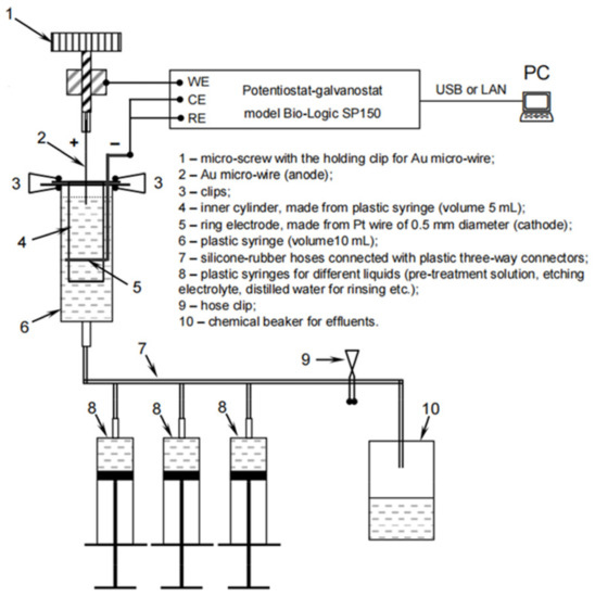
Figure 1.
The principal set-up scheme for the preparation of all-metal Au probes by electrochemical etching of an Au micro-wire in the flow-through electrochemical cell.
The resulting Au probes were washed with deionized water and ethanol (96%), air-dried at room temperature, and glued to a quartz tuning fork (32.768 kHz) before being installed in an AFM-Raman set up for TERS signal acquisition. The quartz tuning forks were soldered to special adapters. Theethyl-2-cyanoacrylate-based adhesive was used for its low viscosity. The rest of the micro-wire from the glued Au probe was cut off by electrical discharge at UDC = 85 V and Imax = 999 mA. The conical end of the all-metal Au probe, glued to the quartz tuning fork, was gently tilted up for 30–35 degrees employing a thin (~0.1 mm of thickness) stainless steel plate.
2.2.4. Preparation of Au TERS Cantilevers by Electrochemical Etching: AFM-Type All-Metal Au TERS Cantilevers
The all-metal Au TERS probes were pre-treated by annealing Au micro-wire (Ø 0.125 mm) at 700 °C for 30 min in a muffle furnace. The Au wire was flattened for2/3 of the length of the ~15 mm long pieces of Au micro-wire between two polished Si wafers to form a flat mirror surface, followed by bending of the remaining part (1/3) of the unflattened part of the pieces of Au micro-wire for ~35 degrees to form the arm of cantilevers (blank all-metal Au cantilever); the ultrasonic decontamination of blank all-metal Au cantilevers was done in warm (40–50 °C) deionized water (up to 5 min), followed by chemical decontamination of the Au micro-wire in the oxidizing mixture of ammonia water NH3·H2O (28%), hydrogen peroxide H2O2 (30%) and ethanol (96%) (volume ratio of components 1:1:4) at room temperature (up to 3 min).
The electrochemical etching was done in an aqueous solution of 5 M (near saturation) of ammonium chloride NH4Cl. The obtained Au probe was washed in distilled water and ethanol (96%) and dried in the air. Electrochemical etching experiments were performed in an electrochemical cell at ambient temperature (20 ± 1 °C), under a voltage in the range from 1.0 to 4.5 V with a sinusoidal waveform frequency of 500 Hz, controlled utilizing a potentiostat/galvanostat BioLogic SP-150. The cut-off moment was controlled manually when the current amplitude dropped to zero.
The obtained Au cantilevers were rinsed with deionized water and ethanol (96%), air-dried at ambient temperature, and after initial examination of the shape and apex of the tip and selection of the probe with the minimal apex diameter, the probe was glued with the appropriate distance between the flattened mirror surface and the tip of the probe to a silicon chip, to be used as a standard AFM cantilever in an integrated AFM/Raman microscope set-up. The low-viscosity ethyl-2-cyanoacrylate-based adhesive was used to glue the cantilever to the silicon chip.
2.3. Evaluation of Prepared Au Cantilevers
Cantilever evaluation was based on visual inspection of the shape and according to parameters such as reproducibility (shape and radius of curvature of the tip), relative enhancement (RE), signal contrast (C), and enhancement factor (EF) of the TERS signal. The repeatability of the resulting Au probe tips was evaluated by measuring the radius of curvature (ROC) of six tips fabricated by the same method [25].
The cantilever’s shape was controlled by lower magnification and resolution Scanning Electron microscopy (SEM) measurements using Scanning Electron Microscope Hitachi TM3000 (Japan). The Scanning Electron microscope Hitachi S-3400N (Hitachi, Hokkaido, Japan) with high magnification and resolution was used for tip apex imaging and analysis.
The evaluation of localized plasmon resonance properties of developed Au cantilevers and application for Raman chemical imaging (mapping) was performed by TERS spectrometer (NTEGRA Spectra, NT-MDT Inc. Appendorf, Nijmegen, The Netherlands) with an “upright” configuration, 100× objective magnification, numerical aperture NA = 1.49, optical beam focus spot diameter of 500 nm. The excitation source used in experiments was the green laser with λ = 532 nm, optical beam power of 25 mW, and beam power on the surface spot of 2 mW.
The evaluation and demonstration of developed cantilevers for biosensing with the submicron resolution were done using hybrid Au/Si cantilevers as Tip-enhanced Raman scattering probes for detection and investigation of the distribution of graphene oxide nanoparticles in Mouse Hepatoma MH-22A cells obtained from Vytautas Magnus University, Biology department Kaunas, Lithuania.
Cell culture preparation was carried out in vitro using mouse hepatoma cell lines (MH-22A). Cells were grown in 25 cm2 tissue culture flasks in DMEM (Dulbecco’s Modified Eagle Medium) supplemented with 10% FBS, 1% L-glutamine, 90 μg/mL streptomycin, and 100 U/mL penicillin (total DMEM) in a humidified atmosphere of 95% air and 5% culture medium, CO2 and at 37 °C. All chemicals were purchased from Sigma-Aldrich (Steinheim, Germany). When the cells reached confluence, they were separated from the bottom of the flask with 1.5 mL of a 0.25% trypsin—0.02% EDTA solution. Then, 2.5 mL of complete DMEM was added to the cell suspension, centrifuged for 2 min at 1000 rpm in a Biosan LMC-3000 centrifuge (Riga, Latvia), and resuspended in 1 mL of complete DMEM.
The methodology of cell sample preparation for AFM, scanning confocal microscopy, and Raman spectroscopy imaging and study is presented below. The 100 μL of the cell suspension (1 × 10⁶ cells/mL) was spread over the surface of the lithium niobate plate into each petri dish filled with 2 mL of complete DMEM. Lithium niobate plates were chosen for their good surface properties for cell growth and subsequent analysis by Raman spectroscopy due to low background signal. The cells were then incubated for 48 h until a monolayer of confluent cells was reached. The control was performed without GO treatment. The GO dispersion was sonicated as described above. GO (12.5 μg/mL) was added to Petri dishes with cells for subsequent incubation. The incubation was done for 24 h, after which the cells were rinsed with ultra-pure water, fixed with 4% formaldehyde (in PBS) for 10 min at room temperature, rinsed again with ultra-pure water, and left to dry for the following microscopic and TERS and Raman spectroscopy investigations.
3. Results and Discussion
3.1. Characterization of Au TERS Cantilevers Prepared by Chemical Deposition Technique
It was observed that the method based on the electroless deposition of Au is quite simple and allows for the fabrication of Au TERS probes with a sufficiently uniform Au coating on the surface of the Si tip and with medium reproducibility of the ROC. SEM images of the uncoated Si tip of a commercial AFM-TERS cantilever and the same tips coated with Au for different electroless deposition times (Figure 2) show that a thick Au coating formed on the surface of the Si tip after 3 min of the electroless deposition process, and the radius of curvature (ROC) of this tip exceeds 200 nm (Figure 2B). Thus, shortening the electroless deposition time up to 2 min allowed for obtaining a gold-coated Si tip with a ROC that decreased by up to ~80 nm (Figure 2C). Shortening the electroless deposition time up to 1 min led to the formation of a smooth Au coating that replicated the cone shape of the Si tip well.
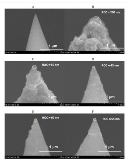
Figure 2.
SEM images of uncoated Si tip (A) and Si tips, coated with Au for different electroless deposition times in an aqueous mixture of 1.0 mM HAuCl4 and 2.0 mM H2OH∙HCl (volume ratio 1:1): 3 min (B), 2 min (C) and 1 min ((D–F), three separate samples). Magnification: 50,000 times.
The calculated mean value and standard deviation (SD) of tip ROC of three Au TERS probes, prepared under the same electroless deposition conditions (Figure 2D–F), are ROCmean = 52.7 nm and SD = 7.1 nm. This indicates that the preparation of Au TERS probes by the chemical electroless deposition method has good reproducibility. The TERS parameters for the Figure 2D cantilever are RE ≈ 20, C ≈ 19, and EF ≈ 2.600.
Relative enhancement of the Raman signal was calculated from the ratio of peak intensities, observed in TERS and micro-Raman spectra of graphene oxide (Figure 3) at 1340–1360 cm−1 (D band) and 1600–1620 cm−1 (G band). The highest relative enhancement of the Raman signal of graphene oxide reaches up to 20 times when such a probe was used for TERS measurements.
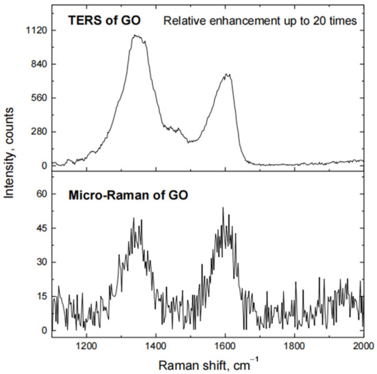
Figure 3.
Raman spectra of GO, when Si tip coated with electroless Au (deposition time 1 min) is in contact with the surface of Si substrate, coated with a film of GO (TERS of GO), and when this tip is retracted from the surface of the substrate (Micro-Raman of GO).
3.2. Characterization of Au TERS Cantilevers Prepared by Sputtering Technique
The fabrication of Au TERS probes using thermal evaporation in a vacuum requires special equipment. However, as seen in Figure 4, this method allows obtaining a very smooth Au coating on the surface of Si tips with a high reproducibility of the coating shape and ROC of the tip. The reproducibility of the thermal evaporation process in terms of the morphology of the Au coating and ROC of the coated tips was evaluated by SEM analysis of three Si probes, obtained by the same thermal evaporation in the vacuum conditions (Figure 4B–D). The calculated mean value and standard deviation (SD) of tip ROC of three Au TERS probes, prepared under the same conditions of thermal evaporation in the vacuum, are ROCmean = 33.0 nm, SD = 2.9 nm. This indicates that the preparation of Au TERS probes by the thermal evaporation method has high reproducibility. TERS parameters for Figure 4B cantilever: RE ≈ 4.5; C ≈3.5; EF ≈ 850 (when AFM set point is 1.0); RE ≈ 8; C ≈ 7; EF ≈ 1.700 (when AFM set point is 1.5); and RE ≈ 12; C ≈ 11; EF ≈ 2.700 (when AFM set point is 2.0).
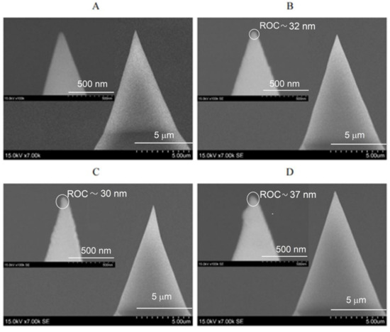
Figure 4.
SEM images of uncoated Si tip (A) and three Si tips, separately coated with Au (B–D) under the same conditions of thermal evaporation in a vacuum. Magnification: (A–D) 7000 times and (insertions of (A–D)) 100,000 times.
The TERS measurements made using the fabricated probes have demonstrated that the Au TERS probes prepared by the thermal evaporation method exhibit a moderate relative enhancement of the Raman signal of graphene oxide by up to 12 times. This value was calculated from the ratio of peak intensities observed in TERS and micro-Raman spectra of graphene oxide (Figure 5) in the 1340–1360 cm−1 and 1600–1620 cm−1 bands (D and G bands, respectively). It was also observed that the relative enhancement of the Raman signal increases with the increasing set-point value at the contact mode of tip-surface interaction (Figure 5). This is related to the decreasing nano-gap between the apex of the Au TERS probe and the surface of the substrate coated with the layer of an analyte, i.e., flakes of graphene oxide, as the AFM set-point parameter increases.
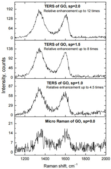
Figure 5.
Raman spectra of GO, when Si probe coated with Au by thermal evaporation in the vacuum technique is in contact with the surface of Si substrate coated with a film of GO (TERS of GO at different values of set point (sp), sp = 1.0, 1.5 and 2.0), and when this probe is retracted from the surface of the substrate (MicroRaman of GO, sp = 0).
3.3. Characterization of Au TERS Cantilevers Prepared by Electrochemical Etching: Shear-Force Type All-Metal Au TERS Cantilevers
The preparation of shear-force type cantilevers with glued-on quartz tuning fork all-metal Au probes, obtained by electrochemical etching of Au micro-wire, is a complex and time-consuming method that requires special equipment and qualified staff. However, the use of a newly developed neutral electrolyte, based on an aqueous solution of ammonium chloride, for electrochemical etching of Au micro-wire allows the fabrication of very sharp all-metal Au probes with high reproducibility of the tip shape and ROC.
The electrochemical reactions that took place on the surface of the anode (Au micro-wire) and cathode (Pt wire ring) during electrochemical etching in NH4Cl electrolyte can be described according to:
| Au(s) + 2Cl−(aq) → [AuCl2]−(aq) + 1e− [AuCl2]−(aq) + 2Cl−(aq) → [AuCl4]−(aq) + 2e− Au(s) + 4Cl−(aq)→ [AuCl4]−(aq) + 3e− | (electrochemical dissolution of Au micro-wire) |
| 2Cl−(aq)→ Cl2(aq) + 2e− | (side reaction) |
| Cathode (–): 2NH4+(aq) + 2e− → 2NH3(aq) + H2(g) | |
It was found that electrochemical etching of Au micro-wire at an alternating voltage in the range from 1.0 to 4.5 V with a sinusoidal waveform frequency of 500 Hz in the newly developed electrolyte, based on an aqueous solution of 5 M NH4Cl, allows very sharp all-metal Au probes (Figure 6) to be calculated. The calculated mean value and standard deviation (SD) of tip ROC of six all-metal Au probes, fabricated under the above-mentioned conditions, are ROCmean = 37.3 nm and SD = 9.4 nm. The aspect ratio (AR) of these probes varies in the range from 1.7 to 2.9. Prepared all-metal Au probes were glued to the quartz tuning forks immediately before they were used for TERS measurements. The conical end of glued all-metal Au probes was inclined to 30–35 degrees to enable the top illumination of the tip by an exciting laser beam. The application of prepared all-metal Au probes with a very sharp tip (ROC < 40 nm) for TERS measurements allowed us to reach a relative enhancement of Raman signal of up to 13 times. This value was calculated from the ratio of the peak intensities observed in TERS and micro-Raman spectra of graphene oxide (Figure 7) at 1340–1360 cm−1 and 1600–1620 cm−1 bands (D and G bands, respectively). TERS parameters for Figure 6E cantilever: RE ≈ 13 C ≈ 12; EF ≈ 3.800.
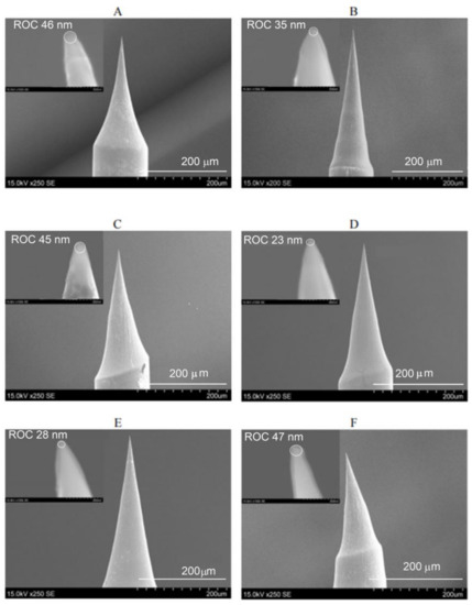
Figure 6.
(A–F) SEM images of six all-metal Au probes, fabricated by electrochemical etching of Au micro-wire in 5 M NH4Cl aqueous solution at an alternating voltage from 1.0 to 4.5 V with a sinusoidal waveform frequency of 500 Hz. Immersion depth of Au wire in electrolyte: ~1.5 mm. Circuit cut-off current: <1 mA. Magnification: (A,C–F) 250×, (B) 200×, (insertions) 150,000×.
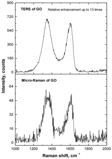
Figure 7.
Raman spectra of GO, when the all-metal Au probe is in contact with the surface of Si substrate, coated with a film of GO (TERS of GO), and when the Au probe is retracted from the surface of this substrate (Micro-Raman of GO).
All-metal Au TERS probes, prepared by the electrochemical etching method, demonstrate moderate relative enhancement of the Raman signal of graphene oxide (up to 13 times).
3.4. Characterization of Au TERS Cantilevers Prepared by Electrochemical Etching: AFM Type All-Metal Au TERS Cantilevers
The preparation of AFM-type cantilevers glued to the silicon AFM chip all-metal Au probes, obtained by electrochemical etching of Au micro-wire, is the most problematic method in terms of reliable control and reproducibility of geometric parameters of a cantilever’s tip. This method also requires special equipment and appropriately qualified staff. SEM analysis revealed that the obtained tips have an apex diameter in the tenths of nanometers with a tip ROC of less than 60 nm (Figure 8). However, a disadvantage of the method is the fabrication problem related to the reproducibility and reliable control of the distance between the tip and the flattened mirror surface of the all-metal Au cantilever. The maximum distance between these two points should not exceed 120 µm (ideal distance ~100 µm) (Figure 8A) to ensure proper alignment of the AFM laser beam to the flattened mirror surface of the Au cantilever for AFM feedback and the laser beam for Raman signal excitation on the tip apex of the all-metal Au probe for TERS measurements. This limitation is due to the technical constraints of the optical system used and the thickness of the all-metal Au cantilever, which determines its mechanical properties. TERS parameters for Figure 8A cantilever: RE ≈ 6 C ≈ 5; EF ≈ 500.
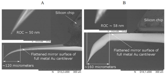
Figure 8.
SEM images of two all-metal Au probes, attached to silicon AFM chips, with proper (A) and improper (B) distance between the tip and the flattened mirror surface of thinner (A) and thicker (B) all-metal Au cantilevers. The tips of these all-metal Au probes were obtained by electrochemical etching in 5 M NH4Cl aqueous solution at an alternating voltage from 1.0 to 4.5 V with a sinusoidal waveform frequency of 500 Hz. Magnification: 300× (insertions 30,000×).
The plasmonic activity of the all-metal Au probe, prepared by the electrochemical etching technique and attached to a silicon AFM chip, was also tested using GO as the target analyte. Raman spectra of GO were obtained with the AFM-type all-metal Au TERS probe in contact with the surface of a Si substrate coated with a film of GO, and when the cantilever was retracted from the surface of the substrate. The results are presented in Figure 9. Au TERS cantilevers prepared by this method demonstrated the lowest relative enhancement of the Raman signal of graphene oxide (up to six times). The low EF can be explained due to the shape and size of the cantilever and possible blockage of the excitation laser beam, preventing the focus of a laser beam on the apex of the tip.
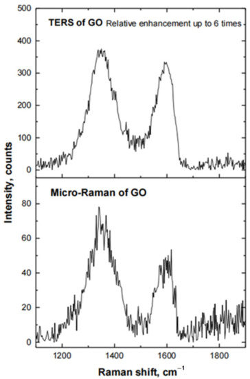
Figure 9.
Raman spectra of GO, when the all-metal Au probe, attached to the silicon AFM chip, is in contact with the surface of Si substrate, coated with a film of GO (TERS of GO), and when the Au probe is retracted from the surface of this substrate (Micro-Raman of GO).
3.5. Comparison of Au TERS Cantilevers
The RE values for Au cantilevers prepared by different methods are presented in Figure 10. The highest enhancement was achieved with Au TERS cantilevers prepared by the chemical deposition technique (up to 20 times; refer to Section 2.2.1 for the method details). The least effective method, due to its low RE, high cost, time consumption, and complexity, is the electrochemical etching method for the fabrication of Au TERS probes, specifically the AFM type all-metal Au TERS cantilevers (refer to Section 2.2.4 for details).
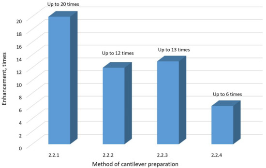
Figure 10.
The comparison of the relative enhancement of Raman signal observed with Au TERS probes prepared by different methods. The presented results respond to analyte molecule GO. The results can vary depending on the analyte molecule type.
The evaluation of probes prepared by four different methods is summarized in Table 1.

Table 1.
The comparison of the methods for the preparation of Au TERS cantilevers.
Au is one of the most commonly used metals for the preparation of TERS probes. It has been observed that TERS technology is rapidly improving and the spatial detection resolution is scaling down to the single-molecule level. Various types of SPM-TERS systems, metal TERS probes, and advanced modalities are being utilized in bio-imaging, medical sensing, etc., and can be further utilized to increase the TERS enhancement level.
Bao et al. used SiO2 nanometer films for coating the Au or Ag TERS tips to enhance their mechanical and chemical stability during experiments, especially during liquid experiments [32]. A newly developed system positions a metal tip on the side of a quartz material tuning fork [29,31]. This novel type of combination of the SERS-TERS system, where the substrate consists of Au and Ag nanoparticles randomly distributed on the substrate surface, can help to reduce the fluorescence background and increase the Raman signal [33].
Furthermore, Wang et al. reported an improvement in the TERS gap mode using Au nanosheets. A gap mode based on the localized surface plasmon resonance effect creates electromagnetic hotspots in the space between the TERS tip and the substrate. The strength of the TERS signaling response correlates with the thickness of the Au nanoplates [34].The enhancing effect of spatial plasmon hybridization was also reported by Chen et al., who found that this assembled TERS system has excellent high-resolution optical imaging capabilities [35]. Ovali et al. developed a new TERS technology using an nm-sized quantum emitter (QE) placed on the metal tip of the AFM, and deposited nanoparticles on the surface of the Si substrate. The researchers found that after illuminating the tip with a femtosecond laser, a plasmon was formed, and the QE-assisted plasmon lifetime increased approximately 17 times [36]. Therefore, the TERS enhancement depends on the parameters of the TERS metal tip, including the tip structure, tip radius, focal radius, and near-field depth and angle of incidence. It is worth noting that all methods are very sensitive, and even small errors can lead to undesirable results.
Top of Form
3.6. Distribution of GO in Mouse Hepatoma MH-22A Cells Measured with Developed Hybrid Au/Si TERS Cantilever
The biochemistry of nanoparticle uptake by cell and distribution inside the cell isa complex mechanism and a still poorly understood phenomenon. Various techniques such as SEM, TEM, and fluorescence microscopy can be used to investigate the mechanism of nanoparticle uptake by the cell. The GO nanoparticles are used as a drug delivery carrier, and Raman imaging is a promising technology to investigate the drug delivery inside the cells in their native environment due to strong Raman activity of GO [37]. The interaction of GO nanoparticles with the cell goes through two phases. During the first phase, the GO nanoparticle is adsorbed from the colloid by the cell membrane, and during the second phase the membrane–cell interaction is managed by several mechanisms of cell biochemistry. It is known that nanoparticles may enter the cell. Internalization of nanoparticles occurs via endocytosis-based mechanisms and was studied in the work [38] using surface-enhanced Raman spectroscopy with gold nanoparticles.
It was shown [39] that adsorbed nanoparticles strongly interact with the cell membrane and that exposure of CHO cells to TiO2 nanoparticles caused morphological changes in the cell membranes and influenced the viability of cells. Therefore, the TERS can be an efficient instrument to investigate the interaction of nanoparticles with the cell membrane. Our experiment aimed to test the possibility of developing TERS probes for the chemical mapping of GO nanoparticles adsorbed on the cell membrane surface. The GO has good biocompatibility; therefore, it was selected as a test material to demonstrate the efficiency of the developed cantilevers for chemical imaging. The Raman imaging of the distribution of GO nanoparticles on the bio-cells membrane was performed on HM22A cells incubated in a GO solution. The hybrid cantilever developed by methodology 2.2.2 was selected. The experimental spectra and TERS signal map is presented in Figure 11.
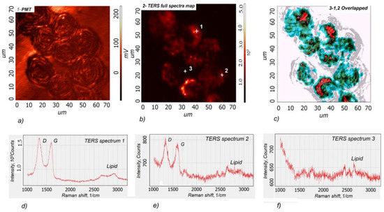
Figure 11.
Scanning laser microscopy image of mouse hepatoma MH-22A cells with adsorbed GO nanoparticles. (a), AFM-based TERS chemical imaging map of GO full spectra (1000–3200 cm−1) (b), the overlapped image of a-b (c), TERS spectra from point 1 (d), TERS spectra from point 2 (e), TERS spectra from point 3 (f). The colors and distribution intensity in Figure 11c correspond to the intensity of the GO TERS signal. The GO nanoparticles were not detected in the white areas. The different-intensity GO spectra were observed in colored areas: the highest GO intensity was detected in the red area and decreasing intensity in the blue areas. The cell’s optical image obtained using scanning laser confocal microscopy is represented by grey color.
The TERS imaging results are consistent with those of other authors who studied the cellular internalization of Au nanoparticle-loaded GO using SERS. GO is heterogeneously distributed on the surface and within cells [40].
4. Conclusions
Four different methods have been proposed for the preparation of Au TERS cantilevers with a nanometric tip ROC.
The novel method of electrochemical etching of Au micro-wire in a non-fuming and harmless neutral electrolyte, based on an aqueous solution of ammonium chloride, allows for the production of sharp all-metal Au probes with high reproducibility of the tip shape and a ROC of less than 60 nm.
The relative enhancement of the Raman signal of graphene oxide was compared using different Au TERS probes fabricated by these four methods.
For a quick and simple preparation of Au TERS probes with medium reproducibility and high relative enhancement of the Raman signal, it is recommended to modify the Si tips of commercial AFM-TERS cantilevers using the chemical (electroless) deposition method.
The advantage of the preparation of Au TERS probes by chemical deposition (galvanic displacement and electroless deposition) is that such a technique does not require specialized and expensive equipment.
A more complex and time-consuming method of preparation of shear-force cantilevers with all-metal Au probes, obtained by an electrochemical etching method, can be reasonably used when higher relative enhancement of Raman signal and/or sensitivity is required during TERS measurements.
The experimental investigation of the developed cantilevers demonstrated the high efficiency of hybrid Au/Si TERS cantilevers. This technique enabled chemical imaging of graphene oxide adsorbed by MH-22A cells.
Author Contributions
Conceptualization and supervision, V.S.; writing—original draft preparation, N.S. and V.S.; data analysis and writing—review, and editing, N.S. and V.S. All authors have read and agreed to the published version of the manuscript.
Funding
This work was funded through a European Space Agency Contract 4000126337/18/NL/SC under the PECS (Plan for the European Cooperating States).
Institutional Review Board Statement
Not applicable.
Informed Consent Statement
Not applicable.
Data Availability Statement
The data presented in this study are available on request from the corresponding author.
Acknowledgments
The view expressed herein can in no way be taken to reflect the official opinion of the European Space Agency. The authors would like to thank L. Traksele and E. Griskonis for their help during the fabrication of TERS probes and for their support to provide experiments.
Conflicts of Interest
The authors declare no conflict of interest.
References
- Li, C.; Huang, Y.; Li, X.; Zhang, Y.; Chen, Q.; Ye, Z.; Alqarni, Z.; Bell, S.E.J.; Xu, Y. Towards practical and sustainable SERS: A review of recent developments in the construction of multifunctional enhancing substrates. J. Mater. Chem. C 2021, 9, 11517–11552. [Google Scholar] [CrossRef]
- Snitka, V.; Batiuskaite, D.; Bruzaite, I.; Lafont, U.; Butenko, Y.; Semprimoschnig, C. Surface-enhanced Raman scattering sensors for biomedical and molecular detection applications in space. CEAS Space J. 2021, 13, 509–520. [Google Scholar] [CrossRef] [PubMed]
- Sonntag, M.D.; Pozzi, E.A.; Jiang, N.; Hersam, M.C.; Van Duyne, R.P. Recent Advances in Tip-Enhanced Raman Spectroscopy. J. Phys. Chem. Lett. 2014, 5, 3125–3130. [Google Scholar] [CrossRef]
- Sharma, G.; Deckert-Gaudig, T.; Deckert, V. Tip-enhanced Raman scattering—Targeting structure-specific surface characterization for biomedical samples. Adv. Drug Deliv. Rev. 2015, 89, 42–56. [Google Scholar] [CrossRef]
- Blum, C.; Opilik, L.; Atkin, J.M.; Braun, K.; Kämmer, S.B.; Kravtsov, V.; Kumar, N.; Lemeshko, S.; Li, J.-F.; Luszcz, K.; et al. Tip-enhanced Raman spectroscopy—An interlaboratory reproducibility and comparison study. J. Raman Spectrosc. 2014, 45, 22–31. [Google Scholar] [CrossRef]
- Mochalov, K.E.; Solovyova, D.O.; Efimov, A.E.; Klinov, D.V.; Oleinikov, V.A. High-performance, reproducible tip-enhanced Raman scattering probes. Tech. Phys. Lett. 2020, 46, 1084–1087. [Google Scholar] [CrossRef]
- Pettinger, B.; Schambach, P.; Villagómez, C.J.; Scott, N. Tip-Enhanced Raman Spectroscopy: Near-Fields Acting on a Few Molecules. Annu. Rev. Phys. Chem. 2012, 63, 379–399. [Google Scholar] [CrossRef] [PubMed]
- Huang, T.-X.; Huang, S.-C.; Li, M.-H.; Zeng, Z.-C.; Wang, X.; Ren, B. Tip-enhanced Raman spectroscopy: Tip-related issues. Anal. Bioanal. Chem. 2015, 407, 8177–8195. [Google Scholar] [CrossRef] [PubMed]
- Rigor, J.; Kurouski, D.; Large, N. Plasmonic Heating Effects in Tip-Enhanced Raman Spectroscopy (TERS). J. Phys. Chem. C 2022, 126, 13986–13993. [Google Scholar] [CrossRef]
- Bonhommeau, S.; Cooney, G.S.; Huang, Y. Nanoscale chemical characterization of biomolecules using tip-enhanced Raman spectroscopy. Chem. Soc. Rev. 2022, 51, 2416–2430. [Google Scholar] [CrossRef]
- Snitka, V.; Rodrigues, R.D.; Lendraitis, V. Novel gold cantilever for nano-Raman spectroscopy of graphene. Microelectron. Eng. 2011, 88, 2759–2762. [Google Scholar] [CrossRef]
- Feng, H.; Xu, C.; Wang, Y.; Wei, Z.; Li, X.; Kan, Y.; Zhang, Y. Effects of electrolyte concentration on the morphology control of gold nanotips in electrochemical etching. J. Appl. Electrochem. 2020, 50, 799–807. [Google Scholar] [CrossRef]
- Foti, A.; Barreca, F.; Fazio, E.; D’Andrea, C.; Matteini, P.; Maragò, O.M.; Gucciardi, P.G. Low cost tips for tip-enhanced Raman spectroscopy fabricated by two-step electrochemical etching of 125 µm diameter gold wires. Beilstein J. Nanotechnol. 2018, 9, 2718–2729. [Google Scholar] [CrossRef] [PubMed]
- Lee, C.; Kim, S.T.; Jeong, B.G.; Yun, S.J.; Song, Y.J.; Lee, Y.H.; Park, D.J.; Jeong, M.S. Tip-enhanced Raman scattering imaging of two-dimensional tungsten disulfide with the optimized tip fabrication process. Sci. Rep. 2017, 7, 40810. [Google Scholar] [CrossRef]
- Yang, B.; Kazuma, E.; Yokota, Y.; Kim, Y. Fabrication of Sharp Gold Tips by Three-Electrode Electrochemical Etching with High Controllability and Reproducibility. J. Phys. Chem. C 2018, 122, 16950–16955. [Google Scholar] [CrossRef]
- Ramanauskaite, L.; Xu, H.; Griskonis, E.; Batiuskaite, D.; Snitka, V. Comparison and Evaluation of Silver Probe Preparation Techniques for Tip-Enhanced Raman Spectroscopy. Plasmonics 2018, 13, 1907–1919. [Google Scholar] [CrossRef]
- Saito, Y.; Murakami, T.; Inouye, Y.; Kawata, S. Fabrication of silver probes for localized plasmon excitation in near-field Raman spectroscopy. Chem. Lett. 2005, 34, 920–921. [Google Scholar] [CrossRef]
- Asghari-Khiavi, M.; Wood, B.R.; Hojati-Talemi, P.; Downes, A.; McNaughton, D.; Mechler, A. Exploring the origin of tip-enhanced Raman scattering; preparation of efficient TERS probes with high yield. J. Raman Spectrosc. 2012, 43, 173–180. [Google Scholar] [CrossRef]
- Rodriguez, R.D.; Sheremet, E.; Müller, S.; Gordan, O.D.; Villabona, A.; Schulze, S.; Hietschold, M.; Zahn, D.R.T. Compact metal probes: A solution for atomic force microscopy based tip-enhanced Raman spectroscopy. Rev. Sci. Instrum. 2012, 83, 123708. [Google Scholar] [CrossRef]
- Fleischer, M.; Weber-Bargioni, A.; Altoe, M.V.P.; Schwartzberg, A.M.; Schuck, P.J.; Cabrini, S.; Kern, D.P. Gold Nanocone Near-Field Scanning Optical Microscopy Probes. ACS Nano 2011, 5, 2570–2579. [Google Scholar] [CrossRef]
- Nemciauskas, K.; Traksele, L.; Salaseviciene, A.; Snitka, V. A silicon membrane-silver nanoparticles SERS chip for trace molecules detection. Microelectron. Eng. 2020, 225, 111282. [Google Scholar] [CrossRef]
- Anderson, M.S. The Detection of Long-Chain Bio-Markers Using Atomic Force Microscopy. Appl. Sci. 2019, 9, 1280. [Google Scholar] [CrossRef]
- Celis, F.; Garcia, M.; Diaz-Fleming, G.; Campos-Vallette, M. A Review of Raman, Surface-Enhanced Raman Scattering (Sers) and Related Spectroscopic Techniques Applied to Biomolecules in Biomaterials. J. Chil. Chem. Soc. 2017, 62, 3627–3632. [Google Scholar] [CrossRef]
- Nicolas Behr, N.; Raschke, M.B. Optical Antenna Properties of Scanning Probe Tips: Plasmonic Light Scattering, Tip-Sample Coupling, and Near-Field Enhancement. J. Phys. Chem. C 2008, 112, 3766–3773. [Google Scholar] [CrossRef]
- Dongmo, L.S.; Villarrubia, J.S.; Jones, S.N.; Renegar, T.B.; Postek, M.T.; Song, J.F. Experiment test of blind tip reconstruction for scanning probe microscopy. Ultramicroscopy 2000, 85, 141–153. [Google Scholar] [CrossRef]
- Cao, Y.; Sun, M. Tip-enhanced Raman spectroscopy. Rev. Phys. 2022, 8, 100067. [Google Scholar] [CrossRef]
- Williams, C.; Roy, D. Fabrication of gold tips suitable for tip-enhanced Raman spectroscopy. J. Vac. Sci. Technol. B Microelectron. Nanometer Struct. Process. Meas. Phenom. 2008, 26, 1761–1764. [Google Scholar] [CrossRef]
- Gao, L.; Zhao, H.; Li, Y.; Li, T.; Chen, D.; Liu, B. Controllable Fabrication of Au-Coated AFM Probes via a Wet-Chemistry Procedure. Nanoscale Res. Lett. 2018, 13, 366. [Google Scholar] [CrossRef]
- Kharintsev, S.S.; Hoffmann, G.G.; Dorozhkin, P.S.; De With, G.; Loos, J. Atomic force and shear force based tip-enhanced Raman spectroscopy and imaging. Nanotechnology 2007, 18, 315502. [Google Scholar] [CrossRef]
- Yang, Y.; Peng, Y.; Lin, C.; Long, L.; Hu, J.; He, J.; Zeng, H.; Huang, Z.; Li, Z.-Y.; Tanemura, M. Human ACE2-functionalized gold “virus-trap” nanostructures for accurate capture of SARS-CoV-2 and single-virus SERS detection. Nano Micro Lett. 2021, 13, 109. [Google Scholar] [CrossRef]
- Kumar, N.; Mignuzzi, S.; Su, W.; Roy, D. Tip-enhanced Raman spectroscopy: Principles and applications. EPJ Tech. Instrum. 2015, 2, 9. [Google Scholar] [CrossRef]
- Bao, Y.-F.; Cao, M.-F.; Wu, S.-S.; Huang, T.-X.; Zeng, Z.-C.; Li, M.-H.; Wang, X.; Ren, B. Atomic Force Microscopy Based Top-Illumination Electrochemical Tip-Enhanced Raman Spectroscopy. Anal. Chem. 2020, 92, 12548–12555. [Google Scholar] [CrossRef]
- Haldavnekar, R.; Venkatakrishnan, K.; Tan, B. Next generation SERS- atomic scale platform for molecular level detection. Appl. Mater. Today 2020, 18, 100529. [Google Scholar] [CrossRef]
- Wang, R.; He, Z.; Sokolov, A.V.; Kurouski, D. Gap-mode tip-enhanced Raman scattering on au nanoplates of varied thickness. J. Phys. Chem. Lett. 2020, 11, 3815–3820. [Google Scholar] [CrossRef] [PubMed]
- Chen, H.; Zhang, Y.; Dai, Y.; Min, C.; Zhu, S.; Yuan, X. Facilitated tip-enhanced Raman scattering by focused gap-plasmon hybridization. Photon. Res. 2020, 8, 103–109. [Google Scholar] [CrossRef]
- Ovali, R.V.; Sahin, R.; Bek, A.; Tasgin, M.E. Single-molecule-resolution ultrafast near-field optical microscopy via plasmon lifetime extension. Appl. Phys. Lett. 2021, 118, 241103. [Google Scholar] [CrossRef]
- Zhang, Z.; Liu, Q.; Gao, D.; Luo, D.; Niu, Y.; Yang, J.; Li, Y. Graphene Oxide as a Multifunctional Platform for Raman and Fluorescence Imaging of Cells. Small 2015, 11, 3000–3005. [Google Scholar] [CrossRef] [PubMed]
- Verma, A.; Stellaci, F. Effect of Surface Properties on Nanoparticle–Cell Interactions. Small 2010, 6, 12–21. [Google Scholar] [CrossRef]
- Batiuskaite, D.; Bruzaite, I.; Snitka, V.; Ramanavicius, A. Assessment of TiO2 Nanoparticle Impact on Surface Morphology of Chinese Hamster Ovary Cells. Materials 2022, 15, 4570. [Google Scholar] [CrossRef]
- Huang, J.; Zong, C.; Shen, H.; Liu, M.; Chen, B.; Ren, B.; Zhang, Z. Mechanism of Cellular Uptake of Graphene Oxide Studied by Surface-Enhanced Raman Spectroscopy. Small 2012, 8, 2577–2584. [Google Scholar] [CrossRef]
Disclaimer/Publisher’s Note: The statements, opinions and data contained in all publications are solely those of the individual author(s) and contributor(s) and not of MDPI and/or the editor(s). MDPI and/or the editor(s) disclaim responsibility for any injury to people or property resulting from any ideas, methods, instructions or products referred to in the content. |
© 2023 by the authors. Licensee MDPI, Basel, Switzerland. This article is an open access article distributed under the terms and conditions of the Creative Commons Attribution (CC BY) license (https://creativecommons.org/licenses/by/4.0/).