Abstract
In this article, we propose a circuit to imitate the behavior of a Reward-Modulated spike-timing-dependent plasticity synapse. When two neurons in adjacent layers produce spikes, each spike modifies the thickness in the shared synapse. As a result, the synapse’s ability to conduct impulses is controlled, leading to an unsupervised learning rule. By introducing a reward signal, reinforcement learning is enabled by redirecting the growth and shrinkage of synapses based on signal feedback from the environment. The proposed synapse manages the convolution of the emitted spike signals to promote either the strengthening or weakening of the synapse, represented as the resistance value of a memristor device. As memristors have a conductance range that may differ from the available current input range of typical CMOS neuron designs, the synapse circuit can be adjusted to regulate the spike’s amplitude current to comply with the neuron. The circuit described in this work allows for the implementation of fully interconnected layers of neuron analog circuits. This is achieved by having each synapse reconform the spike signal, thus removing the burden of providing enough power from the neurons to each memristor. The synapse circuit was tested using a CMOS analog neuron described in the literature. Additionally, the article provides insight into how to properly describe the hysteresis behavior of the memristor in Verilog-A code. The testing and learning capabilities of the synapse circuit are demonstrated in simulation using the Skywater-130 nm process. The article’s main goal is to provide the basic building blocks for deep neural networks relying on spiking neurons and memristors as the basic processing elements to handle spike generation, propagation, and synaptic plasticity.
MSC:
68Q07; 68Q06; 68T05; 68T07
1. Introduction
Neural networks are mathematical models that can be used to approximate functions. They work by adjusting the strengths of connections between neurons, called synaptic weights, based on the difference between the actual output and the desired output. This difference, called the error function, helps the network learn. Different learning rules are used in different contexts, such as control signals in control theory or policies in machine learning. Reinforcement learning (RL) methodologies are useful in tasks where scarcely available reward signals are provided, or the exact relationship between the system’s state vector , the current action , and the reward signal is not reducible to a function (i.e., a model-free system) in a straightforward manner. Generative Adversarial Networks (GANs) involve two neural networks competing for content generation. The goal of the first net is to generate new content (i.e., images, audio) indistinguishable from the training data. The second network assesses the effectiveness of the first one by assigning a score to be maximized. The DDPG [1], TD3 [2], and Soft Actor–Critic [3] neural architectures are advanced control algorithms that use two, three, and even four neural networks working together to produce the best results in control tasks [4]. These algorithms are handy when modeling the system, and creating a proper policy is complicated. However, the training process can be computationally expensive, and conventional von Neumann architectures are not optimal for this task because the storage and processing units are separated from each other, while additional circuitry is required to feed the processor with the necessary data. Spiking Neural Networks (SNNs) attempt to replicate the cognitive mechanisms of biological brains by simulating the dynamics of neurons and synapses, requiring encoding and decoding information as the spiking activity. Neuromorphic computing aims to create hardware that mimics this neuronal model to achieve energy-efficient hardware with high throughput, embedded learning capabilities, and low energy consumption.
The SNN circuit implementation can be in the digital or analog domain. Digital neuromorphic processing involves developing digital hardware that can efficiently solve the differential equations of SNNs. Examples of this type of hardware include Intel’s Loihi [5] and IBM’s Truenorth. This technology has already shown promising results regarding power efficiency and is a research platform compatible with current digital technologies. Digital-to-analog converters (DACs) and analog-to-digital converters (ADCs) are used to quantify or binarize signals. However, using these converters always results in a quantization error, as larger binary words require larger DACs and ADCs, implying that a more significant number of quantization levels would lead to a minor quantization error, but larger circuit implementations without being reflected in better performance [6]. Other frameworks to encode from the analog to the spike domain have emerged, such as PopSAN [7] or the Neural Engineering Framework [8], which are designed to use ensembles of neurons with different sensitivities to encode one single signal into spikes. Both of them are implemented in software or FPGA/GPU platforms.
However, working entirely in the analog domain eliminates the quantization problem by treating information as circuit currents, voltages, charge, and resistance values. This approach allows for implementing neurons in analog counterparts, synapses with memristors, and additional circuitry in crossbar arrays. Using Kirchoff’s laws, values can be added instantaneously.
The conductance in each memristor enables in-memory computing and suppresses the von Neumann bottleneck. Using SNN models to assemble RL architectures can be counterproductive when executed on typical CPUs and GPUs. However, the same models can lead to high-performance and low-energy implementations if executed on neuromorphic devices, especially analog ones. However, as circuit analog design can be a challenging and iterative process, most frameworks/libraries or available tools for SNNs are implemented in current digital technologies. For instance, Nest, SNN Torch, and Nengo [9,10,11] are software libraries that deploy SNNs quickly, but are executed in current CPUs and GPUs. NengoFPGA is a Nengo extension that compiles the network architecture into FPGA devices, which results in a digital neuromorphic hardware implementation. Therefore, most available tools and frameworks for SNNs are currently implemented using existing technologies. Intel’s Lava is a compiler that uploads software-modeled SNNs into a Loihi chip. Both extensions, referred to as frameworks, result in digital neuromorphic implementations that are more efficient than running on von Neumann architectures. However, they are still digital.
The analog implementation of SNNs is still a work in progress in the state of the art, as several articles tackle different building blocks of the SNN (i.e., neurons, synapses, encoders/decoders, etc.). In [12], a population encoding framework for SNNs is presented purely in the analog domain. The framework uses bandpass filters to distribute input signals evenly into input currents for analog neurons. However, storage and learning are not included in this framework. In [13], a Trainable Analog Block (TAB) is proposed that only considers the encoding of signals. Information storage and obtention are left outside the scope of the study, as synapse values are computed offline and stored as binary words. Attending to the latter, in [14], an STDP implementation circuit is presented, by using the charge of capacitors to represent long-term potentiation (LTP) and long-term depreciation (LTD) effects. Another STDP circuit is presented in [15], which uses transconductance amplifiers and capacitors. Neither STDP circuit considers using non-volatile devices, yielding a loss of information once the power supply is out. In [16], a Reward-Modulated STDP synapse is presented, as a 1M4T (one memristor, four transistors) structure. A reward signal voltage is able to route the current direction, which flows through a memristor. The authors of that study then also proposed a GAN SNN in [17], with promising results. However, a generic memristor model was used for the simulation results, which is not synthesizable for manufacturing. To our knowledge, no end-to-end analog neuromorphic framework is available, including encoding, learning, and decoding in purely analog blocks, while using memristive devices as non-volatile storage.
This article presents a novel reward signal synapse circuit designed in the Skywater 130 nm technological node to enable supervised learning in analog SNN circuits. The proposed structure enables a reward signal to switch between potentiation/depreciation of the synapse and spike to be implemented in fully interconnected neuron layers without having loss of power in the spikes, as well as current decoupling, to supply the proper amount of current to the receptor neurons. Section 2 explains the modeling of the SNN and the implementation of the RSTDP learning rule dynamics in the synapse circuit. Section 3 describes the implementation of the memristor model in Verilog-A and the synapse circuit. Section 4 describes the neuron CMOS model used to test the synapse. A neuron network structure is tested in simulation, demonstrating adequate learning capabilities. Section 5 consists of the discussion, conclusions, and future work.
2. Preliminaries
Now, let us proceed by briefly describing the system dynamics of neurons, synapses, and learning algorithms for SNNs in order to understand the resulting circuitry further along the text.
2.1. Spiking Neural Networks
The behavior of biological brains, including the interactions between synapses and neurons, can be mathematically modeled and recreated using equivalent circuitry. One such example is the biological neuron, which has various models that range from biologically plausible, but computationally expensive (such as the Hodgkin and Huxley model [18]), to simplified, yet reasonably accurate models. The leaky integrate and fire (LIF) neuron model simplifies neuron dynamics by approximating the neuron’s membrane as a switched low-pass filter:
In Equation (1), represents the membrane’s voltage, which has specific membrane resistance and capacitance . The temporal charging constant of the neuron imposes a charging/discharging rate as a function of an input excitation current , starting from a resting potential . When overpasses a specific threshold voltage , the neuron emits a spike of amplitude , being the Dirac delta function. As described in [19], by solving the differential equation in the time interval it takes to the neuron from to and considering the frequency definition, a function that relates to the output spiking frequency can be obtained as:
The resulting graph is called a tuning curve [13] and depicts the sensibility of the neurons against an excitatory signal. By varying and , different tuning curves, i.e., spike responses, can be obtained for neurons in the same layer (see Figure 1). For instance, a more significant value for will make the neuron take more time to charge, reducing the spike output frequency and leading to a different tuning curve. This feature can encode the input signals into spiking activity by letting neurons in the same layer have different spike responses for the same input signal (i.e., population encoding).
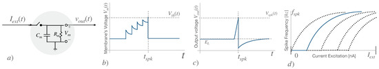
Figure 1.
Leaky integrate and fire model. (a) The LIF model resembles the neuron’s membrane with a capacitance and a resistance values. (b) Each arriving spike contributes to the increase of the membrane’s voltage value , until it reaches the voltage threshold value . (c) Once , the neuron emits a spike at time . (d) The resulting relationship between the injection current and the spike frequency, called tuning curve, can be modified by changing the and values.
2.2. RSTDP Learning Rule
Spike-timing-dependent plasticity (STDP) describes Hebbian learning as neurons that fire together wire together. Given a couple of neurons interconnected through a synapse, the ability to conduct the spikes is controlled by a synaptic weight . The neuron that emits a spike at time is denoted as the pre-synaptic neuron , making the synapse increase its conductance value by a certain differential amount . A spike of current resulting from the convolution of the spike’s voltage through the synapse is produced and fed to a receptor post-synaptic neuron . Each spike contributes to the membrane’s voltage of until it emits a spike at time , then becoming the pre-synaptic neuron, and setting as the time difference between spikes. is then defined as:
For each spike, the synaptic weight will be modified by a learning rate of , multiplied by an exponential decay defined by , respectively. As , the change in the synaptic weight is more prominent. Figure 2b shows the characteristic graph of STDP, showing that, for presynaptic spikes (), the synapse receives LTP, while for post-synaptic spikes (i.e., ), the synapse suffers with LTD. The resulting plasticity rule models how the synaptic weight is modified, considering only the spiking activity. According to [16,20,21], a global reward signal R is introduced to model neuromodulatory signals. Setting , Equation (4) is then changed to:
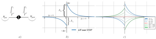
Figure 2.
(a) A presynaptic and a postsynaptic neuron emits spikes, producing Hebbian learning. (b) Spike time-dependent plasticity (STDP) graph, which models the rate of growth () or shrinkage () of the synaptic weight. (c) By introducing a reward signal , the same spikes that produce LTP may produce now LTD. The response curve is shown with different values of R.
Figure 2c shows the role of the reward signal , inverting the role of presynaptic and postsynaptic spikes. Presynaptic spikes now lead to LTD, while postsynaptic spikes lead to LTP. This is the opposite of STDP (i.e., ). Notice that, when , learning (modification of the synaptic weights) is deactivated, as .
3. Materials and Methods
This section describes the necessary circuitry assembled to emulate the models for synapses, neurons, and learning rules.
3.1. Memristor Device
A resistive random-access memory (RRAM) device consists of top and bottom metal electrodes (TE and BE, respectively) enclosing a metal–oxide switching layer, forming a metal–insulator–metal (MIM) structure. A conductive filament starts to be formed with oxygen vacancies when current flows through the device. The distance from the tip of the filament to the opposite bottom electrode is called the gap g. Notice that the length of the filament s is complementary, as the thickness of the oxide layer , as can be seen in Figure 3a. Reverse current increases g, while the device’s resistance increases, and vice versa. Skywater’s 130 nm fabrication process (see [22]) incorporates memristor cells produced between the Metal 1 and Metal 2 layers and can be made using materials that exhibit memristive behavior, such as titanium dioxide (TiO2), hafnium dioxide (HfO2), or other comparable materials based on transition metal oxides.
The RRAM can store bits of information by switching the memristor resistance value between a low resistance state (LRS) and a high resistance state (HRS). However, this work intends to use the whole range of resistance available to store the synaptic weights by directly representing with , with , and any continuous value in between. UC Berkeley’s model [23] defines the internal state of the memristor as an extra node in the tip of the formed filament. The memristor dynamics is described by the current between TE and BE , the rate of growth of the gap , and the local field enhancement factor :
where is the voltage between TE and BE, is the thickness of the oxide separating TE and BE, is the atomic distance, and are fitting parameters obtained from the measurements of the manufactured memristor device [24].
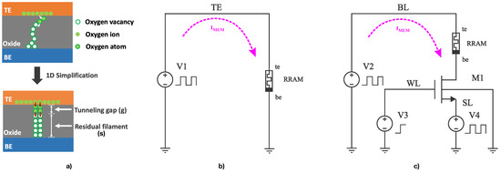
Figure 3.
(a) Lateral diagram of the memristor. Here, oxygen vacancies and ions form a filament of thickness s and a gap g. Extracted from [24]. (b) Test bench used for the first scenario; a triangular pulse from −2 V to 2 V signal is fed. (c) Test bench used for the second scenario, where pulses are applied, using a 1T1R structure.
Then, to introduce a device model as a circuit component in a simulation environment, the user can (a) use SPICE code to reflect the memristor model or (b) describe the device dynamics using Verilog-A, then use the simulator’s compiler, the latter option being the standard. The simulation results described in [25,26,27] show successful transitionary simulations, using 1T1R (one transistor, one resistor) and 1C1R (one capacitor, one resistor) configurations, using the Verilog-A code provided in [28], compiled and simulated with the Xyce/ADMS 7.8 [29] software. However, over these simulations using pulse excitation signals, while they report successful decay in the memristance value, they do not report how the memristance value goes up again by applying pulses in the opposite direction. We could not reproduce the mentioned behavior to the best of our efforts.
It can be noticed in the provided code that the Euler integration method is described, alongside the model, by requesting from the simulator engine the absolute simulation time at each time step with Verilog-A directives such as initial time step or absolute time. At the same time, this works for .tran simulations, but this model description will fail for .op and .dc simulations, where time is not involved, or will lead to convergence simulation issues. These and other bad practices are described in detail by the UC Berkeley team’s article [23]. They provide insight into how to model devices with hysteresis in Verilog-A by properly performing the following:
- Defining TE and BE and the tip of the filament (i.e., g) as electric nodes in Verilog-A. As each node in an electrical circuit possesses properties (voltage, currents, Magnetic Flow, and charge), the compiler knows how to compute the current from the tip of the filament to , by using .
- Providing alternative function implementations for exp() and sinh(), to limit the maximum slope, these can reach between the past and the next time step. Several simulator engines use dynamic time step selection for faster simulation periods and convergence issues. Of course, this limits the minimum time step a simulator can use, but avoids convergence issues or extended execution periods.
- Avoiding the usage of if–then–else statements to set the boundaries for the thickness of the filament. Instead, use a smooth, differentiable version of the unit step function.
This article uses the memristor Verilog-A implementation methodology described in [23], but replaces the manufacturing parameters found in [25,26]. Figure 3a shows a memristor test bench where a triangular signal from −2 V to 2 V is applied, resulting in the Lissajous curve (I–V graph) (Figure 4a), with the typical hysteresis characteristics from memristors, reflecting the V and threshold voltages to increase/decrease the resistance in the device. Figure 4b shows the thickness of the filament, which lies between 4.9 nm and 3.3 nm. On a second test bench depicted in Figure 3b, a 1T1M (one transistor, one memristor) setup is given, where squared pulses (Figure 5a) are applied first at , then at to foster the resistance value exploration, reflecting a proper evolution from LRS to HRS and backward, showing the appropriate previously reported memristance values of the device, that is [10 kΩ, 3.3 MΩ] (Figure 5b). The current flow through the memristor goes from −200 A to 100 A (Figure 5c), matching the obtained Lissajous curve in the previous test bench, alongside the thickness of the filament (Figure 5d). The resulting code is available at our GitHub repository [30], compiled by the OpenVAF tool v.23.5.0 [31]. Simulation results were obtained using Ngspice v. 41 [32].
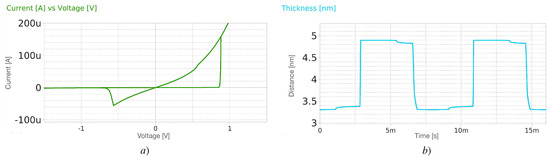
Figure 4.
Memristor simulation scenarios for the first test bench. (a) Lissajous curve (I–V) of the memristor, clearly showing hysteresis and V and , (b) Thickness of the filament s, showing the exponential growth/shrinkage once the memristor threshold voltage is overpassed.
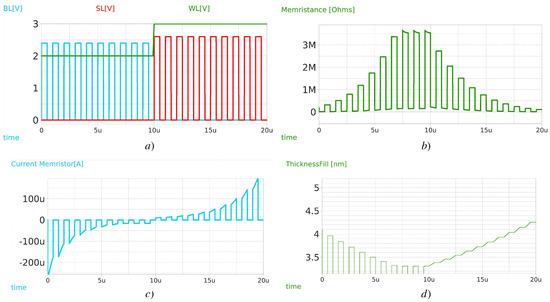
Figure 5.
Memristor simulation scenarios for the second test bench. (a) Voltage pulses applied in the terminals alongside time s. (b) Evolution of the memristance value, going from 10 kΩ to 3.3 MΩ. (c) Current flowing through the memristor, considering positive current when it flows from TE to BE. (d) Evolution of the thickness of the filament s.
3.2. RSTDP Circuit Implementation
Figure 6 shows a 1M4T (one memristor, four transistors) cell replacing the 1T1M cell to manage the current flow of the memristor. Proposed in [17], the structure pretends to invert the current flow according to a reward voltage signal 1.8 V]. When = 1.8 V, transistors and are enabled and and disabled. If , the current will then flow from the BE of the memristor towards the TE. However, when = 0 V, and are disabled and and are enabled, yielding the current direction from the TE to the BE. The current direction determines whether the memristor´s resistance increases or decreases. In Figure 7a, the test bench signals with triangular shapes are applied with a delay of 5 s. Two scenarios are presented: In the first scenario, for the entire simulation, while in the second scenario, flips from 0 V to 1.8 V at 100 s. Notice in Figure 7c,d that the voltage difference () is shown for both scenarios, overpassing the memristor threshold voltage for potentiation. However, when the reward signal is flipped, overpasses the memristor value in the opposite direction. Notice also in Figure 7e,f the magnitude of the spike currents that the memristor delivers, given by the – geometry , which in this case were selected to provide symmetrical pulses of current. However, these aspect ratios can be selected to foster asymmetric STDP curves.
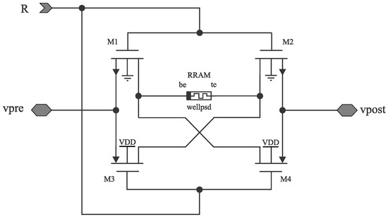
Figure 6.
RSTDP hardware implementation test bench. The 1M4T structure to handle the current direction.
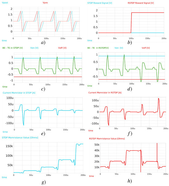
Figure 7.
(a) Applied triangular pulses for and , varying from [0 V, 1.8 V]. Notice that is delayed 5 s from , making . (b) Reward signal R = [0 V, 1.8 V]; to deactivate/activate, drain the gate voltage in the NMOS and PMOS transistors. STDP scenario, with no reward signal (Blue), and the RSTDP scenario, enabling a reward signal in the second half of the simulation. (c,d) Voltage difference between the TE and the BE of the memristor, with and withoud reward signal. Notice that (Blue) and (Red) are overpassed, yielding a modification in the memristance. (e,f) Current flowing through the memristor. (g,h) Obtained memristance values in the STDP and RSTDP scenarios respectively. When activating the reward signal R = 1.8 V (Red), the current now flows in the opposite direction, yielding a reduction in memristance after 100 s.
3.3. Adding Spike Reconformation and Current Decoupling to the Synapse
Now, consider two fully interconnected neuron layers, with N and M neurons needing synaptic connections. When the i -th neuron of the first layer emits a spike, it should be able to provide enough power for the M post-synaptic neurons. Moreover, when the j -th neuron in the second layer emits a spike, it must provide enough power to the N post-synaptic neurons. Consider then the schematic in Figure 8. Notice that the RSTDP structure of the previous section is embedded inside this new structure, supporting the polarity switch according to the arrival of spikes. The port labeled as activates transistors and , making . On the other side, the port labeled as enables transistors and , setting . Then, four scenarios, depicted in Figure 9, emerge:
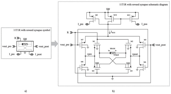
Figure 8.
The 11T1R synapse circuit proposal, including the RSTDP subcircuit. (a) The proposed block, depicting the input/output signals. (b) The internal circuitery for the synapse, the memristor, and the current mirrors for the receiving neurons.
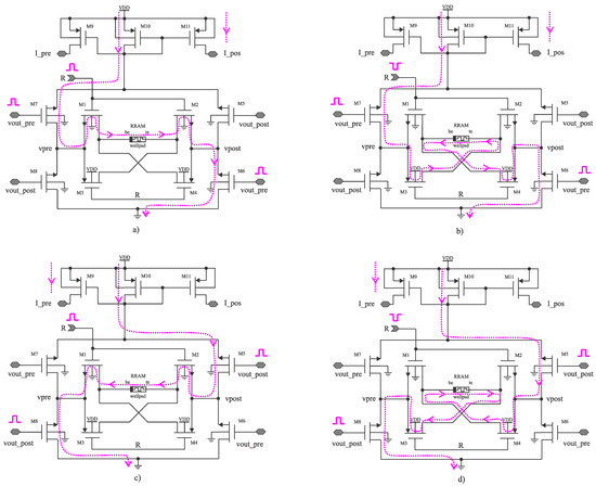
Figure 9.
Proposed synapse circuit, reflecting the four possible scenarios for the evolution of the synaptic weight: (a) V. (b) V. (c) V. (d) V.
- V, when a presynaptic spike arrives and the reward signal is on. This routes the current from the BE to the TE in the memristor, yielding LTD;
- V. Due to the reward signal being negative, the same spike train that should produce LTD now produces LTP, as the current flows from the TE to the BE;
- V. For postsynaptic spikes with the reward signal on, the current flows from the TE to the BE, producing LTP;
- V. For postsynaptic spikes with the reward signal off, the current flows from the BE to the TE, producing LTD.
As the input spikes are pointing toward the transistor’s gates, no current is provided by the neurons. Instead, each synapse only receives the trigger signal (a spike, with an amplitude larger than the threshold value of the transistors) and provides enough current straight from the power source instead of the output node of each neuron. Regarding the upper part of the circuit, it is important to note whether the spike was presynaptic or postsynaptic; the current that flows through transistor always travels from the source to the drain. Additionally, this current is the same one that flows through the memristor, regardless of its polarity. Transistors and then serve as the current mirrors of . When the postsynaptic neuron fires, the current is delivered to the presynaptic neuron by . Then, when a presynaptic spike arrives, feeds the postsynaptic neuron. and are defined as:
As mentioned in the previous sections, the resistance range of the memristor allows it to provide at most 200 uA. However, the input current range of the neuron may differ from the input current ranges the memristor can provide for the same . Therefore, Equations (9) and (10) enable the regulation of the current contribution for each spike.
3.4. Neuron Circuit
Figure 10 depicts the neuron model used in this work, based on the original design by [33], but with some modifications for the avoidance of the output spike to be fed into the same neuron, as seen in [17]. Transistors , and emulate a thyristor with hysteresis by harnessing the fact that the PMOS and NMOS have different threshold voltage values (i.e., ). The circuit dynamics are described as follows:
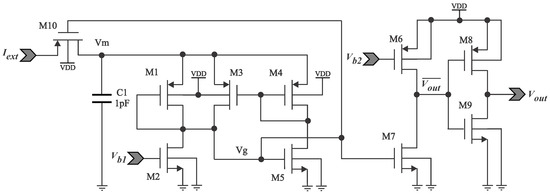
Figure 10.
Analog neuron circuit.
- An external input current excitation arrives through (PMOS), enabled at the start. is set as a diode.
- charges for each incoming spike, increasing the voltage at node .
- A leaky current is flowing though at all times. If no further incoming electrical impulses are received, the neuron will lose all of its electrical charge. defines .
- When V, V, which is the threshold voltage for the NMOS device, enabling the charge to flow through and .
- also turns on, enabling current to flow and making the voltage at drop. At the same time, , turning off transistor , disabling the current integration for the neuron.
- As drops, rises, as works as an inverter. controls the current of the transistor , and conforming to the width of the spike. The node provides the final output spike, which can be fed to subsequent synapses.
- acts as a controlled diode, blocking any current from when the neuron is spiking.
Figure 11 shows the neuron’s spiking activity for an input step signal, which rises each 50 s a step of 50 nA. It can be observed that the frequency increases as more current is added. The amplitude of the output spikes is set as V, but it can be set differently, according to the synapse needs, while the thickness of the spike is approximately 1 ms. The maximum reached spike frequency is kHz, for nA. The neuron output voltage remains at V for bigger input currents. The final design then needs ten transistors. However, notice that can be removed by considering as the output voltage node. The geometry of can be reshaped to regulate its current, defining then the width of the output spike.
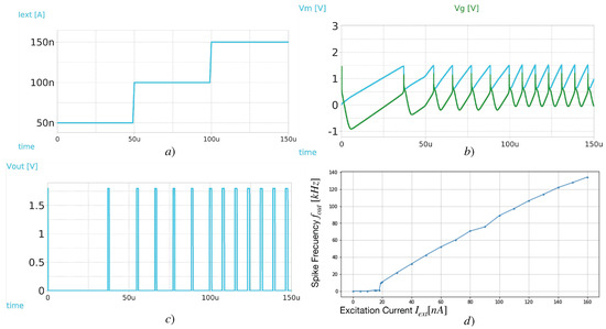
Figure 11.
Simulation results for the analog neuron circuit. (a) Test bench used to supply a step increasing current excitation , starting from 50 nA, 100 nA, and 150 nA (b). When V, it can be seen in (c) that V, turning on transistor , which acts as a charge sink for through . (c) shows the output spikes for each , resulting in a respective frequency of 42 kHz, 89 kHZ, and 128 kHz. (d) Current excitation against spike frequency graph, obtained by sweeping from 0 nA to 160 nA.
4. Results
The test bench shown in Figure 12 intends to test all the capabilities of the proposed synapse by using a 2-1 neuron network array, then using two synapses to interconnect the first layer with the second. During the first half of the simulation, the neurons N1 and N2 in the input layer receive testing excitation currents for each neuron, supported by current mirrors. The neurons at the first layer spike at different rates, as . In the second half of the simulation, the neuron N3 in the output layer receives an excitation current , while the current mirrors for N1 and N2 become deactivated. This should result in long-term potentiation (LTP) for the first half and long-term depression (LTD) in the second half of the execution. However, the reward signal R was set to switch from 1.8 V to −1.8 V at each quarter of the simulation, leading to the four cases previously described.
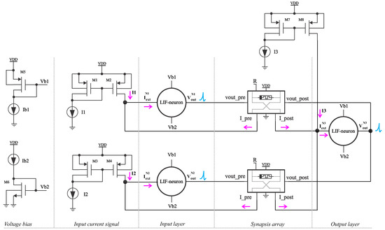
Figure 12.
Test bench to test a 2-1 neuron array, with two neurons at the input layer and one at the input layer.
Figure 13d shows the evolution of the simulation results. In the first quarter, the first case occurs, showing how the thickness of the filament s in the memristor decreases at distinct rates. Remember, as the thickness decreases, so does the conductivity (i.e., LTP is produced). In the second quarter, the same spiking activity led to the opposite effect in the filament, as the reward signal R went from 1.8 V to −1.8 V, leading the thickness to 4.9 nm (i.e., LTD is then produced). In the third quarter, spikes, and and cease to receive excitation current from the current mirrors. With V, the filament should increase in size; however, as its value is already at the maximum, it stays at 4.9 nm. Finally, R flips again to 1.8 V, and the spikes of decrease the filament, obtaining the opposite behavior. Notice the neural activity (spikes), a byproduct of the current integration of incoming spikes of other neurons (see Figure 13c).
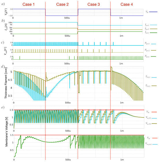
Figure 13.
Simulation results for the test bench are shown, producing the four scenarios (a) Signaling for the reward voltage , which flips from 1.8 V to −1.8 V from quarter to quarter. (b) Excitation current for each of the neurons in the first and second layers. The neurons at the first layer receive 0 nA in the second half of the simulation. (c) Spiking activity for each of the three neurons. Notice that all neurons are able to emit spikes with enough current integration. (d) Thickness of the filament s of each memristor. When it decreases, so does the conductivity. (e) The membrane’s voltage for neurons N1 and N2 in the first layer. Once overpasses a threshold voltage of the neuron, it emits a spike. Notice the difference between the first and second half. The spikes in the second half are a byproduct of the current integration of spikes.
The whole circuit was implemented using Xschem and Ngspice. The geometries for each transistor used for this test bench are described in Table 1. The final list of archives is available at our GitHub repository [30].

Table 1.
Geometries for each transistor used for the test benches described. The scale is set in micrometers 1.
5. Discussion
Next, we point towards some considerations about the obtained circuitry, how this device can be manufactured, and new research opportunities that emerge from this work.
5.1. Regarding the Synapse Circuitry
Table 2 shows a comparison with other STDP circuits proposed in the literature. Some of them use capacitors to store the synapse weight value. Once the power shuts down, the value is missed. Therefore, while feasible for manufacturing, these circuits serve for emulation purposes only. The 1M4T device uses memristors to store the synaptic weight value. Also, in [17], while they did implement a GAN, some blocks like the memristor generic VTEAM memristor mathematical model [34] are not manufacturable. For the circuit presented in this work, the simulation took around
10–15 s for a time step of ns for the implementations, without sudden crashes or singular matrix values in the simulation runtime, due to the well-posed memristor Verilog-A code, the parameters of which have been selected based on the parametrization of a manufactured device. This will enable the simulation of larger deep neural SNNs purely implemented on an integrated circuit. The presented architectures (neuron and synapse) are feasible to manufacture using the Skywater 130 nm process node.
Table 2.
Comparative table with STDP circuits available.
5.2. Future Work Towards Tailor-Made Neuromorphic Computing
The presented blocks then work properly once assembled, leading to the research into how to assemble larger structures. Drawing a schematic of a bigger network with hundreds/thousands of neurons per layer may be problematic, even using the neurons and synapses as sub-blocks, not to mention the layout. Figure 14a shows the resulting layout of the 11T1R synapse structure, comparable in size to the LIF neuron in Figure 14b, drawn in the Magic VLSI EDA 8.3 software [35]. Notice that both structures have internal geometries that might be parameterizable, for instance the length of the current mirrors for in the synapse or the capacitance value for the neuron. As future work, the authors consider that our efforts should focus on automatizing the SPICE files (using programming libraries like PySPICE) for simulation and the GDS files (like implementing PCELLs in TCL scripting) for manufacturing. This will enable research into implementing different deep neural network architectures purely in analog hardware, such as the three-layer LSHDI, interconnected NEF [8], reservoir computing [36] structures, or neural network structures where a reward signal from the environment can be used, such as DDPG, TD3, and SAC implementations using SNNs. As the synapse is originally thought to work as the binding between a presynaptic and a postsynaptic neuron, all the above-mentioned structures are compatible with the synapse.
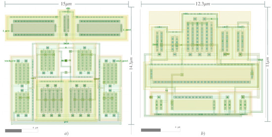
Figure 14.
Layout structure of the described blocks: (a) 11T1R layout structure; (b) LIF neuron structure without the capacitor.
6. Conclusions
This article presents a proper implementation in Verilog-A of the Skywater 130 Reram model, enabling the simulation of the behavior reported in the characterization of the physical device while allowing simulations in shorter periods without convergence issues. Then, a synapse structure, which uses the memristor inside, is presented. This structure enables reward modulation for STDP, decouples the current feeding from the neuron, and successfully transfers the power duties to the synapse. The output spikes of the neuron then do not provide current for the memristor, but only provide the signaling to enable the flow in one direction or the other.
Author Contributions
Conceptualization, A.J.-L.; Data curation, A.J.-L.; Formal analysis, V.H.P.-P. and E.R.-E.; Funding acquisition, H.S.-A.; Investigation, A.J.-L. and V.H.P.-P.; Methodology, A.J.-L. and E.R.-E.; Project administration, H.S.-A. and E.R.-E.; Resources, V.H.P.-P.; Software, O.E.-S.; Supervision, H.S.-A.; Validation, O.E.-S.; Visualization, O.E.-S.; Writing—original draft, A.J.-L.; Writing—review and editing, V.H.P.-P. and H.S.-A. All authors have read and agreed to the published version of the manuscript.
Funding
The authors are thankful for the financial support of the projects to the Secretaría de Investigación y Posgrado del Instituto Politécnico Nacional with grant numbers 20232264, 20242280, 20231622, 20240956, 20232570, and 20242742, as well as the support from Comisión de Operación y Fomento de Actividades Académicas and Consejo Nacional de Humanidades Ciencia y Tecnología (CONAHCYT).
Institutional Review Board Statement
Not applicable.
Informed Consent Statement
Not applicable.
Data Availability Statement
All of the scripts used in this article are available on the following GitHub page: https://github.com/AlejandroJuarezLora/SNN_IPN (accessed on 7 May 2024).
Conflicts of Interest
The authors declare no conflicts of interest.
Abbreviations
The following abbreviations are used in this manuscript:
| ADC | analog-to-digital converter |
| BE | bottom electrode |
| BEOL | Back End Of the Line (manufacturing) |
| CMOS | Complementary Metal–Oxide Semiconductor |
| CPU | Central Processing Unit |
| DAC | digital-to-analog converter |
| DDPG | Deep Deterministic Policy Gradient |
| FPGA | Field Programmable Gate Array |
| GAN | Generative Adversarial Network |
| GDS | Graphic Database System |
| GPU | Graphic Processing Unit |
| HRS | high resistance state |
| IBM | International Business Machines |
| LIF | leaky integrate and fire |
| LRS | low resistance state |
| LTD | long-term depreciation |
| LTP | long-term potentiation |
| MIM | metal–insulator–metal |
| NMOS | Negative Metal–Oxide Semiconductor |
| PCELL | Parametric Cell |
| PMOS | Positive Metal–Oxide Semiconductor |
| RL | reinforcement learning |
| RRAM | Resistive Random Access Memory |
| RSTDP | Reward-Modulated spike-time-dependent plasticity |
| SNN | Spiking Neural Network |
| SPICE | Simulation Program with Integrated Circuit Emphasis |
| STDP | spike time-dependent plasticity |
| TAB | Trainable Analog Block |
| TCL | Tool Command Language |
| TD3 | Twin-Delayed Deep Deterministic Policy Gradient |
| TE | top electrode |
| VTEAM | Voltage Threshold Adaptive Memristor |
References
- Xu, R.; Wu, Y.; Qin, X.; Zhao, P. Population-coded Spiking Neural Network with Reinforcement Learning for Mapless Navigation. In Proceedings of the 2022 International Conference on Cyber-Physical Social Intelligence (ICCSI), Nanjing, China, 18–21 November 2022; pp. 518–523. [Google Scholar] [CrossRef]
- Kim, M.; Han, D.K.; Park, J.H.; Kim, J.S. Motion Planning of Robot Manipulators for a Smoother Path Using a Twin Delayed Deep Deterministic Policy Gradient with Hindsight Experience Replay. Appl. Sci. 2020, 10, 575. [Google Scholar] [CrossRef]
- Lee, M.H.; Moon, J. Deep reinforcement learning-based model-free path planning and collision avoidance for UAVs: A soft actor–critic with hindsight experience replay approach. ICT Express 2023, 9, 403–408. [Google Scholar] [CrossRef]
- Naya, K.; Kutsuzawa, K.; Owaki, D.; Hayashibe, M. Spiking Neural Network Discovers Energy-Efficient Hexapod Motion in Deep Reinforcement Learning. IEEE Access 2021, 9, 150345–150354. [Google Scholar] [CrossRef]
- Akl, M.; Sandamirskaya, Y.; Walter, F.; Knoll, A. Porting Deep Spiking Q-Networks to Neuromorphic Chip Loihi. In Proceedings of the International Conference on Neuromorphic Systems 2021, New York, NY, USA, 27–29 July 2021. ICONS 2021. [Google Scholar] [CrossRef]
- Matos, J.B.P.; de Lima Filho, E.B.; Bessa, I.; Manino, E.; Song, X.; Cordeiro, L.C. Counterexample Guided Neural Network Quantization Refinement. IEEE Trans. Comput.-Aided Des. Integr. Circuits Syst. 2024, 43, 1121–1134. [Google Scholar] [CrossRef]
- Tang, G.; Kumar, N.; Yoo, R.; Michmizos, K. Deep Reinforcement Learning with Population-Coded Spiking Neural Network for Continuous Control. In Proceedings of the 2020 Conference on Robot Learning, Virtual, 16–18 November 2020; Proceedings of Machine Learning Research. Kober, J., Ramos, F., Tomlin, C., Eds.; PMLR: New York, NY, USA, 2021; Volume 155, pp. 2016–2029. [Google Scholar]
- DeWolf, T.; Patel, K.; Jaworski, P.; Leontie, R.; Hays, J.; Eliasmith, C. Neuromorphic control of a simulated 7-DOF arm using Loihi. Neuromorphic Comput. Eng. 2023, 3, 014007. [Google Scholar] [CrossRef]
- Gewaltig, M.O.; Diesmann, M. NEST (NEural Simulation Tool). Scholarpedia 2007, 2, 1430. [Google Scholar] [CrossRef]
- Eshraghian, J.K.; Ward, M.; Neftci, E.; Wang, X.; Lenz, G.; Dwivedi, G.; Bennamoun, M.; Jeong, D.S.; Lu, W.D. Training spiking neural networks using lessons from deep learning. Proc. IEEE 2023, 111, 1016–1054. [Google Scholar] [CrossRef]
- Bekolay, T.; Bergstra, J.; Hunsberger, E.; DeWolf, T.; Stewart, T.; Rasmussen, D.; Choo, X.; Voelker, A.; Eliasmith, C. Nengo: A Python tool for building large-scale functional brain models. Front. Neuroinform. 2014, 7, 48. [Google Scholar] [CrossRef] [PubMed]
- Khan, S.Q.; Ghani, A.; Khurram, M. Population coding for neuromorphic hardware. Neurocomputing 2017, 239, 153–164. [Google Scholar] [CrossRef]
- Thakur, C.S.; Hamilton, T.J.; Wang, R.; Tapson, J.; van Schaik, A. A neuromorphic hardware framework based on population coding. In Proceedings of the 2015 International Joint Conference on Neural Networks (IJCNN), Killarney, Ireland, 12–17 July 2015; pp. 1–8. [Google Scholar] [CrossRef]
- Hazan, A.; Tsur, E.E. Neuromorphic Spike Timing Dependent Plasticity with adaptive OZ Spiking Neurons. In Proceedings of the 2021 IEEE Biomedical Circuits and Systems Conference (BioCAS), Berlin, Germany, 7–9 October 2021; pp. 1–4. [Google Scholar] [CrossRef]
- Yang, Z.; Han, Z.; Huang, Y.; Ye, T.T. 55nm CMOS Analog Circuit Implementation of LIF and STDP Functions for Low-Power SNNs. In Proceedings of the 2021 IEEE/ACM International Symposium on Low Power Electronics and Design (ISLPED), Boston, MA, USA, 26–28 July 2021; pp. 1–6. [Google Scholar] [CrossRef]
- Shi, C.; Lu, J.; Wang, Y.; Li, P.; Tian, M. Exploiting Memristors for Neuromorphic Reinforcement Learning. In Proceedings of the 2021 IEEE 3rd International Conference on Artificial Intelligence Circuits and Systems (AICAS), Washington, DC, USA, 6–9 June 2021; pp. 1–4. [Google Scholar] [CrossRef]
- Tian, M.; Lu, J.; Gao, H.; Wang, H.; Yu, J.; Shi, C. A Lightweight Spiking GAN Model for Memristor-centric Silicon Circuit with On-chip Reinforcement Adversarial Learning. In Proceedings of the 2022 IEEE International Symposium on Circuits and Systems (ISCAS), Austin, TX, USA, 27 May–1 June 2022; pp. 3388–3392. [Google Scholar] [CrossRef]
- Schöfmann, C.M.; Fasli, M.; Barros, M.T. Investigating Biologically Plausible Neural Networks for Reservoir Computing Solutions. IEEE Access 2024, 12, 50698–50709. [Google Scholar] [CrossRef]
- Juárez-Lora, A.; García-Sebastián, L.M.; Ponce-Ponce, V.H.; Rubio-Espino, E.; Molina-Lozano, H.; Sossa, H. Implementation of Kalman Filtering with Spiking Neural Networks. Sensors 2022, 22, 8845. [Google Scholar] [CrossRef] [PubMed]
- Li, X.; Sun, J.; Sun, Y.; Wang, C.; Hong, Q.; Du, S.; Zhang, J. Design of Artificial Neurons of Memristive Neuromorphic Networks Based on Biological Neural Dynamics and Structures. IEEE Trans. Circuits Syst. Regul. Pap. 2024, 71, 2320–2333. [Google Scholar] [CrossRef]
- Akl, M.; Ergene, D.; Walter, F.; Knoll, A. Toward robust and scalable deep spiking reinforcement learning. Front. Neurorobot. 2023, 16, 1075647. [Google Scholar] [CrossRef] [PubMed]
- Hsieh, E.; Zheng, X.; Nelson, M.; Le, B.; Wong, H.S.; Mitra, S.; Wong, S.; Giordano, M.; Hodson, B.; Levy, A.; et al. High-Density Multiple Bits-per-Cell 1T4R RRAM Array with Gradual SET/RESET and its Effectiveness for Deep Learning. In Proceedings of the 2019 IEEE International Electron Devices Meeting (IEDM), San Francisco, CA, USA, 7–11 December 2019; IEEE: Piscataway, NJ, USA, 2019. [Google Scholar] [CrossRef]
- Wang, T.; Roychowdhury, J. Well-Posed Models of Memristive Devices. arXiv 2016, arXiv:1605.04897. [Google Scholar]
- Jiang, Z.; Yu, S.; Wu, Y.; Engel, J.H.; Guan, X.; Wong, H.S.P. Verilog-A compact model for oxide-based resistive random access memory (RRAM). In Proceedings of the 2014 International Conference on Simulation of Semiconductor Processes and Devices (SISPAD), Yokohama, Japan, 9–11 September 2014; pp. 41–44. [Google Scholar] [CrossRef]
- Alshaya, A.; Han, Q.; Papavassiliou, C. RRAM, Device, Model and Memory. In Proceedings of the 2022 International Conference on Microelectronics (ICM), Casablanca, Morocco, 4–7 December 2022; IEEE: Piscataway, NJ, USA, 2022. [Google Scholar] [CrossRef]
- Alshaya, A.; Malik, A.; Mifsud, A.; Papavassiliou, C. Comparison of 1T1R and 1C1R ReRAM Arrays. J. Phys. Conf. Ser. 2023, 2613, 012010. [Google Scholar] [CrossRef]
- Alshaya, A.; Han, Q.; Papavassiliou, C. Passive Selectorless Memristive Structure with One Capacitor-One Memristor. In Proceedings of the 2022 International Conference on Microelectronics (ICM), Casablanca, Morocco, 4–7 December 2022; pp. 121–124. [Google Scholar] [CrossRef]
- Skywater. User Guide 2014; SkyWater SKY130PDK 0.0.0-22-g72df095 Documentation. Available online: https://sky130-fd-pr-reram.readthedocs.io/en/latest/user_guide.html (accessed on 25 April 2024).
- Xyce(™) Parallel Electronic Simulator. [Computer Software]. 2013. Available online: https://helpx.adobe.com/acrobat/using/allow-or-block-links-internet.html (accessed on 25 April 2024).
- Juarez-Lora, A. GitHub—AlejandroJuarezLora. SNN-IPN, MICROSE-IPN. 2024. Available online: https://github.com/AlejandroJuarezLora/SNN_IPN (accessed on 25 April 2024).
- Kuthe, P.; Muller, M.; Schroter, M. VerilogAE: An Open Source Verilog-A Compiler for Compact Model Parameter Extraction. IEEE J. Electron Devices Soc. 2020, 8, 1416–1423. [Google Scholar] [CrossRef]
- Vogt, H. Ngspice, the Open Source Spice Circuit Simulator-Intro— ngspice.sourceforge.io. 2024. Available online: https://ngspice.sourceforge.io/index.html (accessed on 25 April 2024).
- Stoliar, P.; Akita, I.; Schneegans, O.; Hioki, M.; Rozenberg, M.J. A spiking neuron implemented in VLSI. J. Phys. Commun. 2022, 6, 021001. [Google Scholar] [CrossRef]
- Kvatinsky, S.; Ramadan, M.; Friedman, E.G.; Kolodny, A. VTEAM: A General Model for Voltage-Controlled Memristors. IEEE Trans. Circuits Syst. II Express Briefs 2015, 62, 786–790. [Google Scholar] [CrossRef]
- Ousterhout, J.; Hamachi, G.; Mayo, R.; Scott, W.; Taylor, G. Magic: A VLSI Layout System. In Proceedings of the 21st Design Automation Conference Proceedings, Albuquerque, NM, USA, 25–27 June 1984; pp. 152–159. Available online: https://ieeexplore.ieee.org/document/1585789 (accessed on 25 April 2024).
- Hazan, A.; Tsur, E.E. Neuromorphic Analog Implementation of Reservoir Computing for Machine Learning. In Proceedings of the 2022 29th IEEE International Conference on Electronics, Circuits and Systems (ICECS), Glasgow, UK, 24–26 October 2022; pp. 1–4. [Google Scholar] [CrossRef]
Disclaimer/Publisher’s Note: The statements, opinions and data contained in all publications are solely those of the individual author(s) and contributor(s) and not of MDPI and/or the editor(s). MDPI and/or the editor(s) disclaim responsibility for any injury to people or property resulting from any ideas, methods, instructions or products referred to in the content. |
© 2024 by the authors. Licensee MDPI, Basel, Switzerland. This article is an open access article distributed under the terms and conditions of the Creative Commons Attribution (CC BY) license (https://creativecommons.org/licenses/by/4.0/).