Abstract
This article presents a comprehensive and intuitive analysis of the impact of packaging on diode performance and a two-step method for packaging parameter extraction. This is performed using a single forward bias point, one-port measurements and probe tips on a conventional printed circuit board (PCB). A PIN diode was used to validate the method, biased from reverse (−5 V) to forward (1.22 V) bias. Measurements were performed up to 27 gigahertz (GHz). The complete diode characterization process—from the design and the electrical modeling of the test fixture to the extraction of the unpackaged diode measurements—is detailed. The parameters of the package model were extracted, its effects were removed from the measurement, and the behavior of the unpackaged diode was determined. Three operating regions based on their radiofrequency and direct current (RF-DC) behavior were proposed, and an electrical model of the unpackaged diode was derived for each region. The results showed that the influence of the package caused the diode to remain in an unchanged behavior under different biases, indicating that it no longer rectified. The results presented herein are validated by the excellent correlation between the diode’s measured S-parameters, impedance, and admittance and their corresponding models.
1. Introduction
The study of high-frequency devices [1,2,3] has become more relevant in recent years due to the evolution of wireless electronics. Special attention has been given to the study of packaged devices, mainly because package effects that are negligible at low frequencies become significant as the frequency increases and, therefore, must be considered and properly modeled. Among these devices, the diode has attracted special attention, since the parasitic effects introduced by the package can significantly impact its performance when used as a rectifier [1,2,3,4,5,6,7].
The electrical model of a packaged diode can be divided into intrinsic and extrinsic parts. A schematic representation (not to scale) of the cross-sectional view of a packaged diode and its electrical model is presented in Figure 1a and Figure 1b, respectively. The intrinsic part is the device’s innermost aspect, and depends on the biasing conditions (shown in a small green circle in Figure 1a,b). The extrinsic part is independent of the bias, and it interfaces with the external environment and the intrinsic part of the diode. It typically consists of internal connections (shown in the red box, excluding the green circle, in Figure 1a,b) and a dielectric box with external contact pads (shown in the blue box, excluding the red box, in Figure 1a,b). Typically, diode packaging models account for both the internal interconnections and the external contact pads. The electrical model includes inductances and associated with the external metallic contact pads; the pad-to-pad capacitances ( and ); the inductance associated with the internal connections; the capacitance between the internal connections and the pad (); and the series resistance (). The capacitances and model the electrical coupling between the pads over the air and through the substrate, respectively, and are grouped into a single capacitance (which modeled in Figure 1b). Throughout this work, the intrinsic part of the diode is referred to as the unpackaged diode, the extrinsic part as the diode package/packaging, and the complete device (intrinsic + extrinsic) as the packaged diode. The electrical model of the diode’s packaging has been discussed [8,9,10,11,12], yet the influence of packaging on the diode’s performance is still not fully clear.
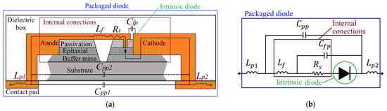
Figure 1.
(a) Schematic representation of the cross-sectional view of a packaged diode and (b) its electrical model. The size of the intrinsic part is about 10 µm, the internal connections are approximately 100 µm, and the packaging box is larger than 500 µm.
Large-signal [7,13] and small-signal [1,2,8,10,11] approaches can be used for modeling and extraction of the diode parameters. The large-signal approach uses voltage and current waveforms to model the diode. In [13], the diode is modeled from S-parameter measurements to extract the extrinsic elements, modeled as lumped components. Meanwhile, the intrinsic part is derived from the current and voltage waveform measurements, in order to obtain equations for internal current sources that model the resistive and capacitive components. In [7], the SPICE model of the diode is derived from I-V and C-V curves, while the extraction of the linear parasitic parameters is performed through S-parameter measurements. The verification of the method is performed through voltage waveforms. Although the methods demonstrate high accuracy ([13], with approximately 10% error), they require both small-signal and large-signal measurements to obtain the full diode model.
The small-signal approach extracts those parasitic elements which are not bias-dependent, using S-parameters from a device (bias-dependent) by polarizing the device at a specific bias. It has previously been applied to transistors [14,15]. In [14], the parameters of the transistor are extracted under the cold condition (Vgs = 0, Vds = 0), based on linear regressions. In [15], the parameters are determined from measurements under the cold condition along with optimization from the hot condition for greater accuracy. Regarding diodes, in [1,2], the extraction of the parameters is performed from a resonance observed in the S-parameters, with 2-port measurement. However, no analysis is presented regarding the significance of this resonance or its impact on the packaging. In [8,10], the impact of the internal diode connections is analyzed, showing their influence in the terahertz range. In [11], the focus has been on modeling the diode as a noise source.
When a commercial packaged diode is acquired from a manufacturer, only the packaged device is available, meaning that measurements are performed on a single structure [2,5,6], and its parameters are obtained by curve fitting. In [2], diode packaging is modeled using a single inductor and a capacitor. In [5], only the total packaging capacitance is extracted from the measurements, while the remaining parameters are optimized by fitting the measured S-parameters. In [6], a numerical optimization method is applied to determine the parameters by curve fitting. Furthermore, the information provided by the manufacturer often includes limited data, which is tested under highly constrained conditions. For instance, if radiofrequency (RF) measurements are performed, the frequency range is typically limited to a few gigahertz (GHz), making it difficult to extrapolate the data to higher frequencies. Rarely is the electrical model of the packaging provided.
Despite all these diode modeling works, none provide an explanation of the individual and combined behaviors of the diode’s intrinsic part and packaging, which is critical to accurately assessing the impact of packaging. However, the analysis requires measurements that intuitively and clearly help in identifying the intrinsic and overall behavior of the diode. The common approach for characterizing diodes is based on two-port measurements [1,2,5,6,7,8]. In such studies, the diode is modeled and compared against its measured S-parameters or its representation on a Smith Chart. Although models and measurements show good agreement, the way measurements and results are presented does not allow clear identification of the intrinsic part response, the packaging response, or the impact of packaging on overall diode performance. Therefore, a clear explanation of both the packaging and the intrinsic diode behavior is essential, with an emphasis on analyzing the packaging’s contribution to the device performance. Furthermore, proposing a practical and straightforward method for parameter extraction from this analysis is required.
This paper presents a contribution to the state-of-the-art by proposing an analysis of the diode’s small-signal behavior across crucial bias points, as well as a two-step parameter extraction method derived from this analysis. The analysis enables differentiation between the contributions of the diode’s intrinsic part and its packaging. To perform the analysis, this work presents measurements using a single port with RF probes on a printed circuit board (PCB). The complete diode characterization process—from the design and the electrical modeling of the test fixture to the extraction of the intrinsic diode model parameters—is detailed. The measurement setup facilitates an intuitive evaluation of the packaging’s impact on the diode’s performance in terms of S-parameters and impedance. The results show that the packaging effect is independent of the bias; consequently, the influence of the package causes the diode to maintain unchanged behavior under different biases, indicating the diode has stopped exhibiting rectifying behavior. The results also illustrate that, in a diode with well-designed packaging, the packaging does not significantly affect the diode’s performance. Conversely, a poorly designed package can substantially degrade the device’s overall behavior.
The rest of the paper is organized as follows. Section 2 details the experimental setup, the design of the de-embedding structures, the diode behavior analysis and the parameter extraction method, while Section 3 shows the extraction of diode package parameters and the results of modeling both the unpackaged and packaged diode. Section 4 discusses the results and addresses key considerations regarding diode measurement. Finally, Section 5 provides the conclusions derived from this work. Appendix A and Appendix B present the electrical models of the de-embedding structures and the unpackaged diode, respectively.
2. Materials and Methods
2.1. Materials
Figure 2a, Figure 2b, Figure 2c and Figure 2d show the measurement setup, and top views of the open structure, the short structure, and the diode soldered onto the test structure, respectively. The measured diode was a PIN diode, CLA4608-085LF. The de-embedding structures were designed using Ansys High-Frequency Structure Simulator (HFSS), while their electrical models were implemented in Advanced Design System (ADS). The structures were fabricated on a Rogers RO3010 substrate with a dielectric permittivity of 10.2, a loss tangent of 0.0022, and thickness of 1.28 mm. The substrate is clad with electrodeposited copper foil of 1/2 oz (18 μm) with roughness of 0.4 μm on the outer surface and 2.0 μm on the dielectric-contacting surface. The structures were fabricated using an LPKF ProtoLaser S4 in collaboration with the PCB prototyping laboratory at CIATEQ Guadalajara. Measurements were performed with an Agilent E8361A PNA Network Analyzer (Agilent Technologies, Santa Clara, CA, USA) and 150 μm Picoprobe RF probes (FormFactor, Inc., Livermore, CA, USA). The test structures were fabricated, and the diode was soldered onto an open structure. Measurements were performed on both the structures and the diode.

Figure 2.
(a) RF device measurement station, and top views of (b) the open structure, (c) the short structure, and (d) the open structure with the diode soldered on it.
To measure the diode using Ground-Signal-Ground (GSG) probe tips, coplanar waveguide (CPW) open and short structures were designed and manufactured. The dimensions that define the impedance of the CPW structure are the width of the central conductor, the gap between the central conductor and the lateral ground planes, and the dielectric height. Using the equations presented in [16] and optimizing by simulation, the open structure (Figure 3a) was designed to maintain a 50 ohm impedance from the beginning of the structure (the probe contact point) to the point where the anode of the diode is connected. Beyond this point, the ground planes were extended and merged, forming the contact for the cathode of the diode. The short structure was implemented by adding a narrow strip that connected the signal line to the ground planes. Figure 3b shows the short structure and its dimensions, while Figure 3c shows the way the diode is connected. An electrical model was proposed for these structures; detailed information is presented in Appendix A.
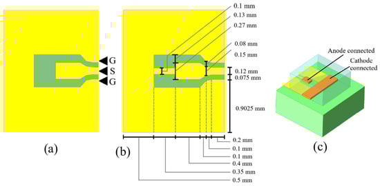
Figure 3.
Top view of the de-embedding structures: (a) open—showing the placement of the RF probe tips; (b) short—showing the dimensions of the structure; and (c) a diode mounted on the open structure.
2.2. Analysis of the Diode’s Small-Signal Behavior Across Crucial Bias Points
Figure 4a–c illustrate the diode’s current vs. voltage (I–V) characteristic curve, the one-port measurement configuration, and the S11 parameters obtained from measurements at three different bias points. Under reverse bias, the diode ideally behaves as an open circuit, while under forward bias, it behaves as an ideal short circuit. At an intermediate bias point, the diode exhibits an impedance close to that of the measurement port (50 Ω). Figure 4a illustrates the position of these operating points on the diode’s I–V characteristic curve. The measured S11 parameter at the three bias conditions using a single-port setup (Figure 4b) are presented in Figure 4c.

Figure 4.
(a) I–V characteristic curve of the diode, (b) single-port measurement configuration, and (c) diode S11 parameters at different bias points (green line: open-circuit condition; black line: short-circuit condition; blue dashed line: impedance close to 50 Ω).
As expected, when the diode behaves as either a short or an open circuit, nearly all the incident energy is reflected to the port, resulting in S11 values close to 0 decibels (dB). Conversely, when the diode’s impedance approaches that of the port, most of the energy is transferred to the diode rather than reflected, leading to a decrease in the S11 parameter, which drops below −10 dB. The variation in the diode’s behavior across different bias points confirms its rectifying operation.
If the S-parameter response remains unchanged with bias, the diode is no longer rectifying. The diode exhibits bias-dependent behavior up to approximately 10 GHz (the manufacturer specifies an operating range up to 6 GHz); however, above 20 GHz, rectification completely ceases; the three lines in the graph exhibit almost the same behavior.
The real and imaginary components of the impedance are shown in Figure 5a,b. The real part of the impedance is different from 50 Ω for the diode operating under open and short-circuit conditions. Conversely, when the diode bias brings its impedance closer to that of the measurement port, the real part of impedance approaches 50 Ω. As observed from the S11 response (Figure 4c) the diode’s behavior at the three bias points becomes practically the same beyond 20 GHz, with a pronounced peak in the real part of the impedance. Since the behavior no longer varies with bias, the diode has stopped rectifying. In the imaginary part, a resonance is observed for all bias conditions above 20 GHz. The peak in the real part of the impedance and the resonance in the imaginary part are parasitic effects of the diode’s packaging, which causes the diode to exhibit a similar behavior across all bias points. The slight shift in the peak and resonance frequencies at the bias points is due to the influence of the diode’s intrinsic region. Although it could be inferred that this effect limits the diode’s rectification frequency, it will be true for some cases, but a more detailed analysis is required to fully confirm this.
Figure 5.
(a) Real part and (b) imaginary part of the diode impedance at the three bias conditions. The green line indicates the open-circuit condition, the black line represents the short-circuit condition, and the blue dashed line corresponds to an impedance approximately equal to 50 Ω.
The resonance can be modeled, its electrical parameters obtained, and its influence can be removed from the measured data to isolate the unpackaged diode behavior, allowing a detailed analysis of the impact of a poorly designed package—where the dominant packaging effect occurs below the intrinsic operating frequency—as presented in the Section 4.
2.3. The Two-Step Parameter Extraction Method
The electrical models shown in Figure 6a,b were used as the basis for parameter extraction. The model’s accuracy is validated in the Section 3, while the analysis of the model is presented in the Section 4. Ideally, the intrinsic part of the diode behaves as an open circuit under reverse bias and as a short circuit under forward bias; therefore, the circuit in Figure 6a can be approximated by the diode model in Figure 6b for forward bias. The diode in short-circuit at forward bias (DSFB) is a bias point in which the diode behaves as a short circuit under forward bias, and it can be selected at a voltage higher than the knee voltage, making sure the device can withstand the potential difference without being damaged. This value can be determined either by the manufacturer or from laboratory measurements.
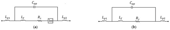
Figure 6.
Electrical model of the diode used in this work, (a) with intrinsic part (The intrinsic diode region is represented as Int box.) and (b) approximation on forward bias.
The model for the diode’s package is derived through a two-step process by measuring S-parameters at the DSFB point and converting them to impedance () and admittance (). Under forward bias, , , and are determined from the diode’s (Step 1), while is extracted from its (Step 2).
2.3.1. Step 1, Obtaining , , and
Figure 6b illustrates the diode model in forward bias. The impedance behavior of the diode in forward bias () as a function of frequency is given by
where corresponds to the sum of and , since and are connected in series. The imaginary part of the equation can be written as
From (2), it can be observed that has a significant impact at the resonance frequency, diminishing as the frequency deviates from resonance. Furthermore, the resonance frequency is solely determined by the contribution of and , and it is independent of . can be approximated by neglecting in Equation (2) to:
The diode reactance can be an be rewritten by dividing both terms by :
From (4), an equation with three variables is obtained. By selecting three different frequencies, a system of three equations with three variables is obtained.
The lowest frequency value is selected so that ≪ , allowing the approximation , resulting in:
The highest frequency value is selected at the maximum impedance point (the resonance frequency), which occurs when :
The intermediate frequency is selected at a point between the lowest and highest frequency and is evaluated using (4).
2.3.2. Obtaining
As in [10], is obtained from in forward bias when → 0
3. Results
Measurements of the diode were performed from reverse bias (−5 V) to forward bias (1.22 V). Parameter extraction was performed at 1.22 V, which is considered the DSFB point. This value was selected based on manufacturer data and laboratory measurements. The manufacturer specifies that the diode can withstand 100 mA. Laboratory measurements showed that this current was reached at a bias of 1.22 V. Figure 7 shows the experimental I–V curve of the diode.

Figure 7.
Measured I–V curve of the diode showing the conduction regions determined by its RF behavior, as proposed in this work. Blue solid line in linear scale (left axis) and blue dashed line in logarithmic scale (right axis). In the logarithmic scale for negative currents (when V < 0), the absolute value is used for plotting. In the non-conduction region, the diode behaves as an open circuit; in the full-conduction region, the diode acts as a short circuit; in the semi-conduction region, the diode’s impedance nears the measurement port impedance (50 ohms).
Diode Packaging Parameter Extraction
The method proposed in Section 2 was implemented to model the diode’s package. The diode was biased at 1.22 V, and the parameters were determined from the graph in Figure 8. The extraction used point A for (5), point B for (4), and point C for (6), making a system of three equations with three unknowns (extraction A-B-C).
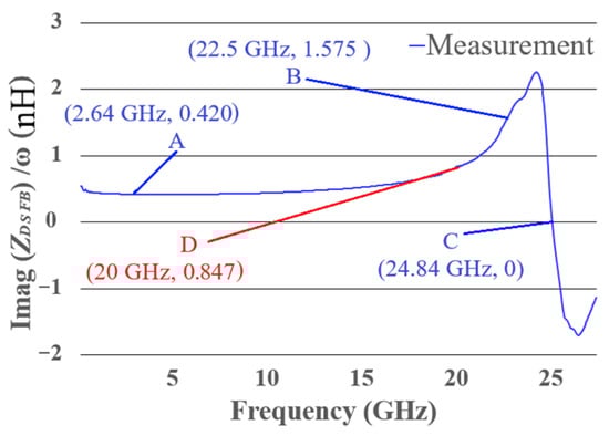
Figure 8.
of the diode measurement (at 1.22 V). Points A, B, and C are used for parameter extraction (extraction A-B-C). Point D (red line) is used for further analysis of the method (extraction A-B-D).
To demonstrate the impact of using Equation (6) without reaching the resonance frequency, a second extraction was carried out. The second extraction used point A for (5) and points B and D for (4) at two different frequencies as two different equations, setting another system of three equations with three unknowns (extraction A-B-D).
The extracted parameters are presented in Table 1. The imaginary part of the impedance, obtained from measurements at DSFB, along with the electrical model from Figure 6b using the values obtained from both parameter extractions (A-B-C and A-B-D), is shown in Figure 9.

Table 1.
Values obtained from the resonant extraction.
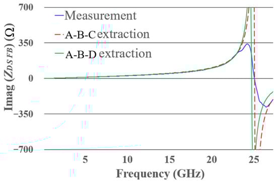
Figure 9.
from diode measurements (at 1.22 V) and the model shown in Figure 2b with extraction A-B-C and A-B-D.
As expected, the A-B-C extraction shows good correlation in (Figure 9) at frequencies below and above the resonance frequency. To further explore the method, the A-B-D extraction is implemented, showing a good correlation even at frequencies below the resonance. This indicates that the method can still be effectively applied when the test frequency is below resonance, yielding reliable results.
Packaged Diode vs. Unpakaged Diode
Removing the parasitic elements of the diode package was performed as in [6] and is shown in Figure 10, thus obtaining the unpackaged diode. Since it is a PIN diode, the intrinsic part can be represented by up to four electrical models [17,18,19,20], each corresponding to different bias regions of the diode.
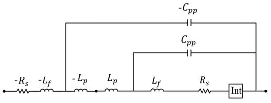
Figure 10.
Removal of packaging parasitic effects from the diode measurements to isolate the unpackaged diode [6].
Whereas other works use direct current (DC)-measured I–V curves as a reference to determine the diode’s operating regions, in this article, the operating regions are determined by its RF behavior. The operating regions are defined as follows: In the non-conduction region, the diode operates as an open circuit. The impedance across frequency will be higher compared to the port impedance, dominated by a large imaginary part. The corresponding DC values for this behavior range from −5 V to 0.3 V. In the semi-conduction region, the diode operates as a load matched to the port. The impedance across frequency will be close to the port impedance, dominated by a real part close to 50 ohms. The corresponding DC values for this behavior range from 0.4 V to 0.6 V. In the full-conduction region, the diode operates as a short circuit. The impedance across frequency will be close to zero (both real and imaginary parts). The corresponding DC values for this behavior range from 0.7 V to 1.22 V. The corresponding frequency range for the three regions extends up to 6–10 GHz. Figure 7 shows the diode’s operating regions, determined by its RF behavior but illustrated on the diode’s I–V curve. The models of the unpackaged diode for the different operating regions are presented in Appendix B.
The S11 for the three operating regions of the unpackaged diode, obtained from both the model and measurements, are presented in Figure 11. Figure 11a corresponds to the bias values ranging from −5 V to 0.3 V, Figure 11b corresponds to the bias values between 0.4 V and 0.6 V and Figure 11c corresponds to the bias values from 0.7 V to 1.22 V. Good agreement between the measured data and the model is observed.

Figure 11.
S11 parameters of the (a) non-conducting, (b) semi-conducting and (c) full-conducting regions of the unpackaged diode.
After modeling the unpackaged diode, the package elements are added to complete the full diode model (packaged diode).
The S11 for the three operating regions of the packaged diode, obtained from both the model and measurements, is presented in Figure 12. Figure 12a corresponds to the bias values ranging from −5 V to 0.3 V, Figure 12b corresponds to the bias values between 0.4 V and 0.6 V and Figure 12c corresponds to the bias values from 0.7 V to 1.22 V. Good agreement between the measured data and the model is observed.

Figure 12.
S11 parameters of the (a) non-conducting, (b) semi-conducting and (c) conducting regions of the packaged diode model.
4. Discussion
4.1. Analysis of the Effect of Packaging Parasitic Elements on Diode Performance
Figure 13 shows the diode behavior in terms of S-parameters (Figure 13a), the imaginary part of the impedance (Figure 13b), and the real part of the impedance (Figure 13c), at a bias of 0.5 V, under five conditions: the intrinsic diode (solid blue line); the packaged diode with the values extracted in Section 3 (dashed blue line, labeled as nominal); and the packaged diode with modified values of , at 6 nH (dashed brown line), at 1 nH (dashed purple line), and at 0.8 pF (dashed red line). 0.5 V bias is selected, as it enables a more intuitive interpretation of the diode’s behavior on S parameters. The first objective of the analysis is to compare the behavior of the intrinsic diode with that of the packaged diode (i.e., the intrinsic diode plus the packaging parasitics) and to understand why removing the parasitic elements does not result in a significant change in the S-parameters. The second objective is to evaluate the individual effect of each of the three packaging parasitic elements (, , and ) by varying them separately to observe their impact on diode performance. Finally, the effect of is analyzed in detail by evaluating its impact at 0.5 V, −5 V (diode off), and 1.22 V (diode conducting) to assess its influence across the diode’s three operating regions.

Figure 13.
(a) S-parameters and (b) imaginary and (c) real part of the impedance of the diode at 0.5 V bias, on five different conditions: Intrinsic diode, nominal packaged diode, , modified to 6 nH, modified to 1 nH and modified to 0.8 pF.
4.1.1. Comparison Between Unpackaged and Packaged Diode
The S-parameter behavior of the intrinsic diode shown in Figure 13a, at frequencies below 6 GHz, exhibits good impedance matching to the port (with values below −10 dB). As frequency increases, the diode becomes mismatched, reaching values close to 0 dB. The packaged diode shows no significant change compared to the intrinsic diode in S parameters. The difference becomes evident when analyzing the impedance.
The real part of the intrinsic diode’s impedance (Figure 13c) stays close to 50 Ω below 6 GHz and decreases as frequency increases. In an ideal diode, the real part of the impedance would remain constant across frequency. In practice, however, the real part of the impedance decreases with increasing frequency. This behavior may result from design characteristics, material limitations, fabrication imperfections or junction capacitance. The imaginary part follows a straight line with a slight slope. The packaged diode shows similar behavior below 6 GHz; however, at 25.8 GHz, a resonance appears in the imaginary part (Figure 13b), along with a peak in the real part (Figure 13c). Both effects are centered at 25.8 GHz and are caused by the packaging parasitics.
From this analysis, it is determined that the diode behavior below 6 GHz is dominated by its intrinsic part, while at higher frequencies, it is dominated by the packaging. For the specific scenario analyzed, the packaging effects do not meaningfully impact the diode’s rectification performance, since the maximum operating frequency of the intrinsic part is lower than the frequency at which the packaging exhibits its dominant influence. This agrees with the information provided in the manufacturer’s datasheet. It is the expected behavior of a well-designed packaged diode, where parasitic elements do not significantly affect performance. Only a small variation is observed in the S-parameters (Figure 13a) at the frequencies where packaging effects start to dominate. It is important to emphasize, however, that this effect should be considered to accurately determine the actual impedance value.
When the packaging is not well designed and the parasitic effects (inductance and capacitance) are higher, the resonances in the impedance appear at lower frequencies, affecting the diode’s behavior where only intrinsic effects should be present. This case is analyzed below. It is important to emphasize that when the matching results from the impedance of the intrinsic part of the diode, it varies with bias. In contrast, when the matching results from the impedance of diode packaging, it appears at all bias points, interfering with the diode’s rectifying behavior.
4.1.2. Impact of an Increase in on Packaged Diode Behavior at 0.5 V
In this and the following analyses, the packaged diode with parasitic values extracted in the Section 3 is compared against packaged diodes with modified parasitic elements. From this point forward, the diode with extracted values will be referred to as the nominal diode.
In this case, is set to 6 nH. In the impedance plots (Figure 13b,c), the resonance shifts from 25.8 GHz (nominal diode) to 5.4 GHz, a frequency where intrinsic behavior should dominate. From the S-parameters (Figure 13a), the diode is matched at 973 MHz with −25 dB, but this changes to −2.2 dB at 3.48 GHz. This behavior occurs because the imaginary part of the impedance crosses zero (matching) and then increases rapidly (mismatch). The mismatch at 3.48 GHz indicates that the packaging has lowered the operating frequency, since this effect will appear at all bias points.
4.1.3. Impact of an Increase in on Packaged Diode Behavior at 0.5 V
In this analysis, is set to 1 nH. In the imaginary part of the impedance (Figure 13b), the resonance shifts upward compared to the nominal diode, while the real part (Figure 13c) shows no noticeable change. In the S-parameters, the diode is matched at 2.55 GHz with −13.7 dB, and at 9.1 GHz, the matching changes to −2.2 dB. This behavior occurs because the imaginary part of the impedance crosses zero (matching) and then increases (mismatch). The mismatch at 9.1 GHz indicates that the packaging has lowered the operating frequency, since this effect will appear at all bias points.
4.1.4. Impact of an Increase in on Packaged Diode Behavior at 0.5 V
In this analysis, is set to 0.8 pF. In impedance (Figure 13b,c), the resonance shifts to 15.88 GHz and its magnitude decreases, allowing the diode to match with the port. As a result, the S-parameters show this second resonance as a matching point (Figure 13a). This is a packaging effect and, although its impact is the opposite to the previous two cases, it also limits the diode’s operating frequency.
4.1.5. Impact of an Increase in on Packaged Diode Behavior at −5 V, 0.5 V and 1.22 V
To demonstrate how = 0.8 pF limits the operating frequency across all bias points, Figure 14 shows the S-parameters of packaged diodes at different bias conditions.
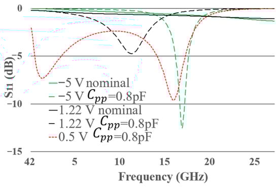
Figure 14.
S-parameters of packaged diodes at different bias points and package conditions. The bias points considered are: −5 V nominal, −5 V with = 0.8 pF, 1.22 V nominal, 1.22 V with = 0.8 pF, and −0.5 V with = 0.8 pF.
As in the previous section, the term nominal refers to the curves whose packaging parameters are those extracted and listed in Table 1. The bias points considered are: −5 V nominal, −5 V with = 0.8 pF, 1.22 V nominal, 1.22 V with = 0.8 pF, and −0.5 V with = 0.8 pF (this last point was analyzed in the previous section).
As expected, the −5 V and 1.22 V nominal plots remain close to 0 dB, since they represent an open circuit and a short circuit, respectively. In the plots for −5 V, −0.5 V, and 1.22 V with = 0.8 pF, a matching point appears at 16.8, 15.88, and 11.1 GHz. The frequency shift of these matchings is due to the combined effects of the diode’s intrinsic part and the packaging. Since the matchings appear across all bias points, the diode is not rectifying but instead acting as a partially matched load to the port, which is an undesired behavior. In the diode packaging, changes in inductance can be associated with the size of the pads and internal interconnections, while changes in capacitance may result from variations in the size and spacing of the contact pads.
In summary, the behavior of both the unpackaged diode and its packaging can be analyzed in terms of polarization and frequency. With respect to polarization, the impedance of the unpackaged diode will depend on the polarization, while the impedance of the diode package will remain independent of it. In terms of frequency, the unpackaged diode will exhibit its rectifying behavior up to a maximum frequency, whereas the diode package shows a frequency at which it has its greatest contribution. If the maximum operating frequency of the unpackaged diode is lower than the frequency at which the packaging exhibits its dominant influence, the packaging effects do not meaningfully affect the diode’s rectification performance. On the contrary, if the maximum operating frequency of the unpackaged diode is higher than the frequency at which the packaging exhibits its dominant influence, the packaging will considerably affect the diode’s rectification performance, reducing the maximum frequency at which the diode can rectify.
4.2. Expectations on Diode Measurements
Diode measurements can be analyzed by the S11 parameter graph in dB, interpreting the Smith Chart, and comparing the impedance and admittance responses.
The expected S-parameter behavior under single-port measurements at various bias points is illustrated in Figure 11 and Figure 12. In the non-conducting region, the diode behaves as an open circuit (Figure 11a and Figure 12a), whereas in the conducting region, it acts as a short circuit (Figure 11c and Figure 12c). In both cases, the S11 values are close to 0 dB. The most informative behavior, however, occurs during the transition between these two states. As the diode begins to conduct, its impedance gradually decreases, eventually approaching the 50 ohm impedance of the measurement port. At this point, proper impedance matching is achieved, enabling maximum RF power transfer to the diode. This condition is observed in Figure 11b and Figure 12b, where peak power transfer occurs at a bias of 0.5 V.
In addition to the S-parameters in dB, the magnitude and phase of the models should exhibit strong correlation. Figure 15 shows the magnitude and phase of the S-parameters for the packaged diode across the three operating regions.
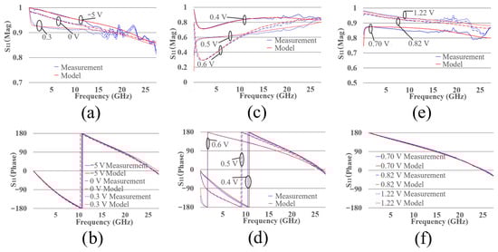
Figure 15.
S11 parameter of the measurement and electrical model of the packaged diode at different bias points. (a) magnitude and (b) phase from −5 V to 0.3 V, (c) magnitude and (d) phase from 0.4 V to 0.6 V and, (e) magnitude and (f) phase from 0.7 V to 1.22 V.
The Smith Chart corresponding to a measurement at 0.4 V is presented in Figure 16. Figure 16a shows the raw data, Figure 16b illustrates the results after de-embedding the open and short structures, whereas Figure 16c displays the response after removing the packaging parasitics. A consistent match across these stages is expected to validate the de-embedding process and parasitic extraction.

Figure 16.
Smith Chart of the diode at 0.4 V bias. The measured data are shown in blue, and the proposed model is shown in red. (a) Packaged diode with measurement structure, (b) packaged diode, and (c) unpackaged diode.
In Figure 16c (unpackage diode), it is observed that the impedance is entirely located at the bottom half of the Smith chart, indicating that it is dominated by capacitive reactance, which can be attributed to the junction capacitance. In Figure 16b (packaged diode), it is observed that part of the diode’s impedance has shifted to the upper part of the Smith chart, indicating that the packaging of the diode has introduced this inductive reactance, which can be attributed to the metallic pads and internal connections. Finally, in Figure 16a (raw diode), it is observed that part of the diode’s impedance has shifted to the lower half of the Smith chart again, indicating that the de-embedding structures introduce an additional capacitive reactance. This behavior can be attributed to the high permittivity of the de-embedding structures
Figure 17 presents the impedance and admittance curves of the diode, both with packaging and the intrinsic model only. To ensure that a proposed intrinsic electrical model accurately represents the physical device, the simulated impedance and admittance must match those obtained from measurement.

Figure 17.
(a) , (b) , (c) , and (d) of the packaged diode at 0.4 V bias. (e) , (f) , (g) , and (h) of the intrinsic part of the diode at 0.4 V bias. The measured data are shown in blue, and the proposed model is shown in red.
In summary, S11 parameters in dB help verify the correct diode operation across different bias points. The Smith Chart provides insight into the diode’s behavior as an open or short circuit and confirms consistency throughout the de-embedding and parasitic extraction stages. Finally, impedance and admittance analyses play a key role in validating the proposed models
4.3. Packaging Electrical Model
One of the most comprehensive models for diode packaging is presented in [10], with its schematic representation provided in Figure 18. The intrinsic region is represented by the Int box, and its electrical model varies depending on the diode type (PN junction, PIN, Schottky). The rest of parameters belong to the extrinsic part of the diode. Despite its apparent completeness, the model incorporates components that are not physically associated with the diode.
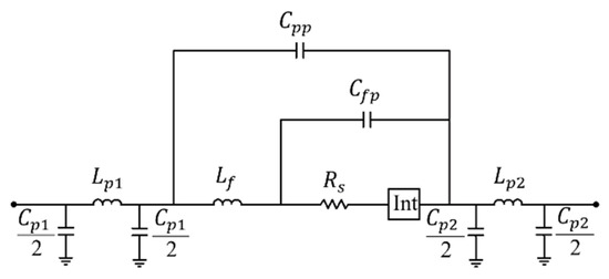
Figure 18.
Electrical model of the diode based on [10]. The intrinsic diode region is represented as Int box. In [21], it is demonstrated that and are not part of the diode model.
The capacitors and of the π-networks represent parasitic capacitances between the contact pads and the ground planes. These components are not part of the diode but arise from the measurement setup itself. Specifically, in two-port configurations, whether microstrip or CPW, both the anode and the cathode are connected to the signal path, and and emerge as parasitic elements between the pads soldered to the signal trace and ground. The calculations of and have been addressed by [21], who demonstrated that the values of and vary significantly depending on the substrate used during characterization. Such variability confirms that these capacitances are not inherent to the diode package but are parasitic effects introduced by the two-port measurement setup. Moreover, this conclusion can be easily validated by implementing the model in a shunt configuration by grounding one of the terminals: in this setup, /2 (or /2) becomes immediately shorted and additionally, a parallel LC ( and /2) network is formed, further reinforcing the assertion that these elements originate from the measurement setup and not from the physical structure of the diode. Once this distinction is established, the π-network structures at both ends of the circuit can be simplified to two inductors, and . These inductors are in series with the rest of the packaging model and can be combined into a single equivalent inductance, . The capacitance of the diode’s internal connections has been analyzed using electromagnetic simulations and the design of specialized structures in [22,23]. It has been observed that its value is around a few fF, significantly lower than that of . Furthermore, the effects of , due to its small value, are noticeable in the THz range [23]. As a result, it may be disregarded, as evidenced by the graphs presented throughout this work, where the model used accurately replicates the packaged diode measurements.
4.4. Method Limitations
One of the requirements for applying the method is that resonances must be measurable, which requires high-frequency measurements. However, in the Section 3, a second parameter extraction (A-B-D extraction) is performed at a frequency lower than the resonance frequency, demonstrating a good correlation between the model and the measurement up to the frequency where the highest point was chosen for the extraction, as shown in Figure 9.
In [11], measurements of Schottky diodes of various sizes are performed in a single-port configuration up to a frequency of 325 GHz. In the impedance graphs presented, resonance can be observed, which demonstrates that the resonance is a generalized behavior present in different types of diodes and at higher frequencies. This indicates that the method presented throughout this work can be applied to different types of diodes and even to higher frequencies.
4.5. Future Research Directions
The next steps in the research are: first, to analyze the behavior of the diode’s linear and nonlinear elements under stress conditions, such as temperature and electromagnetic coupling; and second, to observe the diode’s operation within a system. Some approaches that are already starting to analyze ideas include those based on time-domain [24,25]. A time-domain approach is presented in [24], where the diode is analyzed as part of a rectifier circuit, where diode reverse conduction, temperature and load are included in the model. In [25], a time-domain state-space model is proposed for modeling rectifiers, using a combination of ordinary differential equations and a semi-discrete electromagnetic system to represent the interaction between the rectifier and the electromagnetic fields. The following investigations should be directed in that direction, establishing models of the device under stress conditions and proposing experiments that can reliably verify the models.
5. Conclusions
This work presented a simple and effective method for extracting the parasitic packaging parameters in diodes, demonstrating that the packaging can be modeled using three elements: the pad-to-pad capacitance (), the pad inductance (), and the internal connection inductance (). These parameters can be determined from the resonance observed in the diode’s reactance.
It was shown that in devices with a well-designed package, the packaging effects do not significantly impact the performance of the diode’s intrinsic part. In contrast, poorly designed packaging can limit its rectification operating frequency, by making the diode exhibit similar behavior across all bias points.
Furthermore, the combined analysis of DC and RF measurements allowed the identification of three operating regions of the diode based on its frequency response, which can be categorized into non-conduction, semi-conduction, and full conduction regions, each of which requires a distinct electrical model. Lastly, the importance of properly modeling the de-embedding structures, particularly the open structure, was highlighted, as its inductive and capacitive effects, related to the substrate’s high permittivity and physical dimensions, impact meaningfully at both low and high frequencies.
Author Contributions
Conceptualization, H.A.C.-H. and R.S.M.-A.; methodology, H.A.C.-H. and R.S.M.-A.; software, H.A.C.-H. and R.S.M.-A.; validation, H.A.C.-H. and R.S.M.-A.; formal analysis, H.A.C.-H. and R.S.M.-A.; investigation, H.A.C.-H. and R.S.M.-A.; resources, H.A.C.-H. and R.S.M.-A.; data curation, H.A.C.-H. and R.S.M.-A.; writing—original draft preparation, H.A.C.-H. and R.S.M.-A.; writing—review and editing, H.A.C.-H. and R.S.M.-A.; visualization, H.A.C.-H. and R.S.M.-A.; supervision, H.A.C.-H. and R.S.M.-A.; project administration, H.A.C.-H. and R.S.M.-A.; funding acquisition, R.S.M.-A. All authors have read and agreed to the published version of the manuscript.
Funding
This research was funded by the Mexican Secretariat for Science, Humanities, Technology and Innovation (Secihti), grant number 852217.
Institutional Review Board Statement
Not applicable.
Informed Consent Statement
Not applicable.
Data Availability Statement
The original data presented in the study are openly available in CLA4608-085LF_S11_DIFERENTE_BIAS at https://github.com/HidaiArnulfoCardenasHerrera/CLA4608-085LF_S11_DIFERENTE_BIAS.git (8 December 2025).
Acknowledgments
The authors thank Noe Ariza for his help during the measurements, as well as Martha Alejandra Mogollan Jimenez and Israel Martinez Silva with the PCB prototyping laboratory at CIATEQ Guadalajara, Mexico, for the manufacturing of the test structures.
Conflicts of Interest
The authors declare no conflicts of interest. The funders had no role in the design of the study; in the collection, analyses, or interpretation of data; in the writing of the manuscript; or in the decision to publish the results.
Abbreviations
The following abbreviations are used in this manuscript:
| PCB | printed circuit board |
| GHz | gigahertz |
| RF-DC | radiofrequency and direct current |
| HFSS | High-Frequency Structure Simulator |
| ADS | Advanced Design System |
| GSG | ground-signal-ground |
| CPW | coplanar waveguide |
| I–V | current vs. voltage |
| DSFB | diode in short-circuit at forward bias |
Appendix A. Electrical Model for the De-Embedding Structures
The electrical models of the open and short de-embedding structures are presented in Figure A1. The proposed open model in (Figure A1a) consists of an inductor () in series with a capacitor (), both connected in series with an arrangement of three branches: (i) , (ii) in series with and , and (iii) . The short model (Figure A1b) is obtained by adding an inductance () and a resistance () to the open model, as indicated by the dashed lines.

Figure A1.
Electrical models of the de-embedding structures: proposed (a) open model and (b) series arrangement of and added (as indicated by the dashed lines) to the open structure to fully model the short structure.
Figure A1.
Electrical models of the de-embedding structures: proposed (a) open model and (b) series arrangement of and added (as indicated by the dashed lines) to the open structure to fully model the short structure.

Figure A2 shows the real part of the impedance () of the open structure obtained from simulation, measurement, and the proposed electrical model in this article. The agreement between simulation and measurement validates the method. The high capacitive effect of the structure at low frequencies is attributed to the high permittivity of the substrate, which is necessary to achieve the required pitch for the measurement probes, as well as to the large size of the structure.
As shown in Figure A2, the behavior of the designed open structure can be divided into three frequency regions: low, mid, and high frequencies.
- At low frequencies, tends to be infinite, as expected for an open circuit
- At mid frequencies, becomes approximately constant.
- At high frequencies, increases due to the combination of the inductive and resistive effects of the open structure.
In the proposed model, the infinite at low frequencies is represented by the resistor , the minimum at mid frequencies is represented by the resistor , and the increase in at high frequencies is represented by . The transition from infinite at low frequencies to low at mid frequencies is modeled by the capacitor , and the increase in from mid to high frequencies is represented by the inductor .

Figure A2.
of the proposed open structure, obtained through simulation, measurement, the model proposed in this work, and the classical model.
Figure A2.
of the proposed open structure, obtained through simulation, measurement, the model proposed in this work, and the classical model.

In order to extract the parameters of the electrical model of the open structure, the following considerations must be made: The in the electrical model for the open is influenced solely by the three-branch arrangement, since and are in series with the three-branch arrangement and thus only affect the imaginary part of the impedance. At low frequencies, the of the three-branch arrangement is dominated by and , while at high frequencies, it is dominated by , , and , with 15 GHz as the threshold between low and high frequencies. The electrical model of the open structure is obtained in three steps, as follows: the circuit with , , and is created, and their values are calculated (first step); once obtained, and are added to the circuit, and their values are calculated (second step); finally, and are added to the circuit, and their values are calculated (third step). The first step involves determining , , and from at high frequencies. The real component of the impedance for the , , and arrangement is given by:
From this, it can be observed that the shape of the curve is influenced by and , while acts as an offset. In Figure A3, the behavior of the || arrangement is shown by the dashed green line, which is parallel to the at high frequencies. Additionally, an enlargement of a segment of both curves is observed in the graph, highlighting the difference between them. Thus, through curve fitting, and are extracted by modeling a curve parallel to , while is obtained from the difference between the two curves.

Figure A3.
of the proposed open structure, from measurement, the model without and and .
Figure A3.
of the proposed open structure, from measurement, the model without and and .

In the second step, and are added to the circuit. Theoretically, the impedance of an open circuit tends to approach infinity at low frequencies, and is intended to replicate this behavior. To assign its value, is determined from the maximum value of , measured at low frequencies. is obtained by fitting the curve between 3 and 9 GHz. In the third step, and are added to the circuit and determined by curve fitting of the susceptance ( on Figure A4).
For the short, and (Figure A1b) are obtained by removing the effects of the open structure from the short structure, using the formula for low frequencies.
where
and

Figure A4.
Susceptance of the open structure from measurements; the proposed electrical model and the model without and The effect of and shifts down the susceptance value.
Figure A4.
Susceptance of the open structure from measurements; the proposed electrical model and the model without and The effect of and shifts down the susceptance value.

The S11 parameters from simulation, measurement, and the proposed electrical model of the open and short are presented in Figure A5. Table A1 shows the extracted values of the elements of the proposed model. Since parameter extraction is carried out in a straightforward manner, this model is easier to implement than other models [26,27].

Figure A5.
S11 parameter of the measurement, simulation and proposed electrical model of the open (a) dB, (b) magnitude, (c) phase and short (d) dB, (e) magnitude, (f) phase structures.
Figure A5.
S11 parameter of the measurement, simulation and proposed electrical model of the open (a) dB, (b) magnitude, (c) phase and short (d) dB, (e) magnitude, (f) phase structures.

It is worth noting that there is a difference in the values of capacitance () of the short (0.113 pF) and open structures (0.35 pF). This is attributed to the fact that for the open the electric field is distributed without a closed conductive path, allowing for greater charge accumulation and therefore, higher capacitance. In contrast, the short presents a closed path for the electric field, thus reducing charge accumulation, resulting in a lower capacitance.
Table A1.
Values of the open-short of the classic and proposed electrical models.
Table A1.
Values of the open-short of the classic and proposed electrical models.
| Parameters | Value | Parameters | Value |
|---|---|---|---|
| 0.004279 nH | 0.181 pF | ||
| 0.113/0.35 pF | 0.31 Ohm | ||
| 0.477 nH | 0.172 nH | ||
| 0.012 Ohm | 24 KOhm | ||
| 400 Ohm |
Appendix B. Electrical Model for Unpackaged Diode Under Three Bias Operation Regions
Figure A6 presents the electrical model for these three regions. In this study, three different models were identified to represent the PIN diode in its three operating regions:
- In the non-conduction region, the electrical model (Figure A6a) corresponds to the bias values ranging from −5 V to 0.3 V.
- In the semi-conduction region, the electrical model (Figure A6b) corresponds to the bias values between 0.4 V and 0.6 V.
- In the full-conduction region, the electrical model (Figure A6c) corresponds to the bias values from 0.7 V to 1.22 V.
Upon removing the package elements, the electrical models of the non-conducting and semi-conducting regions are those presented in Figure A6; when the diode behaves as an open circuit, the model consists of an inductor (), a capacitor (), and a series combination of a resistor () and a capacitor () connected in parallel with a second resistor () that represents the high-resistance behavior at low frequencies. In the semi-conducting region, a second branch consisting of a capacitor (), a resistor (), and an inductor (), is added to account for the effect of the depletion region on the intrinsic part of the PIN diode [20]. The electrical model of the conducting region (Figure A6c) consists of two resistors ( and ), which represent the diode’s resistance at low and high frequencies, respectively, and a capacitor and an inductor ( and ) that model the transition between these impedance levels. The extracted values for the intrinsic parameters of the diode are presented in Table A2 and Table A3. From Table A2, it can be noted that, due to the addition of a third branch in the second region of the diode, the elements and will be reduced in value since the added second branch ( or ) will dominate.

Figure A6.
Electrical model of the intrinsic part of the diode in the (a) non-conduction, (b) semi-conduction, and (c) full-conduction regions.
Figure A6.
Electrical model of the intrinsic part of the diode in the (a) non-conduction, (b) semi-conduction, and (c) full-conduction regions.

Table A2.
Values of the intrinsic diode in non-conducting and semi-conducting region.
Table A2.
Values of the intrinsic diode in non-conducting and semi-conducting region.
(V) | (Ohm) | (pF) | (nH) | (pF) | (Ohm) | (nH) | (Ohm) | (pF) |
|---|---|---|---|---|---|---|---|---|
| −5 | 129 | 0.5 | 0.055 | 8 | 1 | - | - | - |
| 0 | 1350 | 1 | 0.055 | 1 | 1.5 | - | - | - |
| 0.3 | 389 | 1.05 | 0.055 | 0.85 | 1.5 | - | - | - |
| 0.4 | 1030 | 4 | - | 1.5 | 250 | 0.055 | 2 | 0.5 |
| 0.5 | 440 | - | 0.040 | 3.8 | 60 | 0.015 | - | 0.5 |
| 0.6 | 53.8 | - | 0.015 | 18 | 17.1 | 0.02 | - | 0.6 |
Table A3.
Values of the intrinsic diode in conducting region.
Table A3.
Values of the intrinsic diode in conducting region.
| Bias (V) | (Ohm) | (pF) | (pF) | (nH) |
|---|---|---|---|---|
| 0.7 | 7.381 | 4.5 | 100 | - |
| 0.82 | 1.7 | 0.5 | - | 0.078 |
| 1.22 | 1.31 | 0.1 | - | 0.05 |
References
- Luo, H.; Hu, W.; Guo, Y. Parameter extraction and modeling of Schottky diodes: An extension of the resonance based inductance extraction method. In Proceedings of the IEEE MTT-S International Wireless Symposium, Nanjing, China, 23–26 May 2021; pp. 1–3. [Google Scholar] [CrossRef]
- Luo, H.; Li, J. A novel extraction method for series inductance in Schottky diodes based on resonance. In Proceedings of the IEEE MTT-S International Microwave Workshop Series on Advanced Materials and Processes for RF and THz Applications (IMWS-AMP), Suzhou, China, 29–31 July 2020; pp. 1–3. [Google Scholar] [CrossRef]
- Amirpour, R.; Schwantuschke, D.; Van Raay, F.; Brueckner, P.; Quay, R.; Ambacher, O. Large-signal modeling of a scalable high-Q AlGaN/GaN high electron-mobility varactor. IEEE Trans. Microw. Theory Tech. 2019, 67, 922–927. [Google Scholar] [CrossRef]
- Bendjeddou, I.; Garcia, M.J.; El Valli, A.S.; Litvinenko, A.; Cros, V.; Ebels, U.; Jenkins, A.; Ferreira, R.; Dutra, R.; Morche, D.; et al. Electrical modeling of spin-torque diodes used as radio frequency detectors: A step-by-step methodology for parameter extraction. IEEE Trans. Microw. Theory Tech. 2023, 71, 2771–2781. [Google Scholar] [CrossRef]
- Gao, S.-P.; Hu, W.; Zhang, H.; Guo, Y. Millimeter-wave rectifiers using proprietary Schottky diodes: Diode modeling and rectifier analysis. In Proceedings of the Wireless Power Week (WPW), Bordeaux, France, 5–8 July 2022; pp. 180–184. [Google Scholar] [CrossRef]
- Hansen, J.; Chang, K. Diode modeling for rectenna design. In Proceedings of the IEEE International Symposium on Antennas and Propagation (APSURSI), Spokane, WA, USA, 25 August 2011; pp. 1077–1080. [Google Scholar] [CrossRef]
- Chen, Q.; Chen, X.; Cai, H.; Chen, F. Schottky diode large-signal equivalent-circuit parameters extraction for high-efficiency microwave rectifying circuit design. IEEE Trans. Circuits Syst. II Express Briefs 2020, 67, 2722–2726. [Google Scholar] [CrossRef]
- Tang, A.Y.; Stake, J. Impact of eddy currents and crowding effects on high-frequency losses in planar Schottky diodes. IEEE Trans. Electron Devices 2011, 58, 3260–3269. [Google Scholar] [CrossRef]
- Zhang, Y.; Wu, C.; Liu, X.; Wang, L.; Dai, C.; Cui, J.; Li, Y.; Kinar, N. The development of frequency multipliers for terahertz remote sensing system. Remote Sens. 2022, 14, 2486. [Google Scholar] [CrossRef]
- Tang, A.Y.; Drakinskiy, V.; Yhland, K.; Stenarson, J.; Bryllert, T.; Stake, J. Analytical extraction of a Schottky diode model from broadband S-parameters. IEEE Trans. Microw. Theory Tech. 2013, 61, 1870–1878. [Google Scholar] [CrossRef]
- Ghanem, H.; Gonçalves, J.C.A.; Chevalier, P.; Alaji, I.; Aouimeur, W.; Lepilliet, S.; Gloria, D.; Gaquière, C.; Danneville, F.; Ducournau, G. Modeling and analysis of a broadband Schottky diode noise source up to 325 GHz based on 55-nm SiGe BiCMOS technology. IEEE Trans. Microw. Theory Tech. 2020, 68, 2268–2277. [Google Scholar] [CrossRef]
- Umbach, P.; Thome, F.; Leuther, A.; Quay, R. Unified scalable model for HEMT-based planar Schottky diodes. IEEE Trans. Microw. Theory Tech. 2025, 73, 1424–1436. [Google Scholar] [CrossRef]
- García-Luque, A.; Mata-Contreras, F.J.; Martín-Guerrero, T.M. Analysis, Formulation, and Implementation of a Nonlinear Equivalent Circuit for High-Frequency Semiconductor Diodes. IEEE Microw. Mag. 2025, 26, 25–41. [Google Scholar] [CrossRef]
- Torres-Torres, R.; Murphy-Arteaga, R. Straightforward Determination of Small-Signal Model Parameters for Bulk RF-MOSFETs. In Proceedings of the Fifth IEEE International Caracas Conference on Devices, Circuits and Systems, Punta Cana, Dominican Republic, 3–5 November 2004; Volume 1, pp. 14–18. [Google Scholar] [CrossRef]
- Gibiino, G.P.; Santarelli, A.; Cignani, R.; Traverso, P.A.; Filicori, F. Measurement-Based Automatic Extraction of FET Parasitic Network by Linear Regression. IEEE Microw. Wirel. Compon. Lett. 2019, 29, 598–600. [Google Scholar] [CrossRef]
- Wolff, I. Coplanar Microwave Integrated Circuits; Wiley: Hoboken, NJ, USA, 2006. [Google Scholar]
- Bera, S.C. Microwave Active Devices and Circuits for Communication; Springer: Cham, Switzerland, 2019. [Google Scholar]
- Hao, X.; Zhang, A.; Gu, G.; Liang, S.; Song, X.; Zhang, L.; Xu, P.; Gao, J.; Feng, Z. GaAs PIN diode-based 220 GHz switch design using flip chip technique. IEEE Trans. Terahertz Sci. Technol. 2025, 15, 100–106. [Google Scholar] [CrossRef]
- Tantwai, K.K. Microwave-frequency non-linear universal model for PIN diode. In Proceedings of the International Workshop on Physics of Semiconductor Devices (IWPSD), Mumbai, India, 16–20 December 2007; pp. 119–122. [Google Scholar] [CrossRef]
- Zhang, A.; Gao, J. Comprehensive analysis of linear and nonlinear equivalent circuit model for GaAs-PIN diode. IEEE Trans. Ind. Electron. 2021, 69, 11541–11548. [Google Scholar] [CrossRef]
- Ladan, S. Simultaneous Wireless Power Transmission and Data Communication. Ph.D. Dissertation, École Polytechnique de Montréal, Montreal, QC, Canada, 2014. [Google Scholar]
- Nadri, S.; Xie, L.; Jafari, M.; Bauwens, M.F.; Arsenovic, A.; Weikle, R.M. Measurement and extraction of parasitic parameters of quasi-vertical Schottky diodes at submillimeter wavelengths. IEEE Microw. Wirel. Compon. Lett. 2019, 29, 474–476. [Google Scholar] [CrossRef]
- Xu, H.; Schoenthal, G.S.; Liu, L.; Xiao, Q.; Hesler, J.L.; Weikle, R.M. On estimating and canceling parasitic capacitance in submillimeter-wave planar Schottky diodes. Microw. Wirel. Compon. Lett. 2009, 19, 807–809. [Google Scholar] [CrossRef]
- Trevisoli, R.; Da Paz, H.P.; Da Silva, V.S.; Casella, I.R.S.; Capovilla, C.E. Modeling Schottky Diode Rectifiers Considering the Reverse Conduction for RF Wireless Power Transfer. IEEE Trans. Circuits Syst. Part II 2022, 69, 1732–1736. [Google Scholar] [CrossRef]
- Odiamenhi, M.A.; Basherlou, H.J.; See, C.H.; Parchin, N.O.; Goh, K.; Yu, H. State-Space Modelling of Schottky Diode Rectifiers Including Parasitic and Coupling Effects up to the Terahertz Band. Electronics 2025, 14, 3718. [Google Scholar] [CrossRef]
- Sánchez-Muñoz, J.P.; Torres-Torres, R. Characterization of bias-dependent ceramic capacitors from reflection coefficient measurements performed using a VNA. IEEE Trans. Electromagn. Compat. 2024, 66, 351–358. [Google Scholar] [CrossRef]
- Roy, C.; Wu, K. A generalized circuit model development approach with short open thru (SOT) de-embedding technique and its applications. IEEE Trans. Microw. Theory Tech. 2024, 72, 124–137. [Google Scholar] [CrossRef]


Disclaimer/Publisher’s Note: The statements, opinions and data contained in all publications are solely those of the individual author(s) and contributor(s) and not of MDPI and/or the editor(s). MDPI and/or the editor(s) disclaim responsibility for any injury to people or property resulting from any ideas, methods, instructions or products referred to in the content. |
© 2025 by the authors. Licensee MDPI, Basel, Switzerland. This article is an open access article distributed under the terms and conditions of the Creative Commons Attribution (CC BY) license (https://creativecommons.org/licenses/by/4.0/).