Abstract
A zero-ripple input current is known to improve the lifetime of battery sets and fuel cells and to assure maximum power point tracking in PV panels. To perform current ripple elimination in a floating interleaved boost converter (FIBC), one of the typical linear inductors is substituted by a variable inductor, and phases of the converter have complementary duty cycles. This variable inductor is controlled using a switched current-source converter, which adjusts the input current ripple. An equivalent model for the variable inductor is presented, including uncertainties in the component description. To achieve current stabilization, a variable inductor controller was designed using the sliding modes approach via fixed frequency. An experimental prototype is implemented and tested with an output voltage controller to compare with the conventional FIBC. The results demonstrate that the input current ripple of the proposed converter is eliminated without significantly decreasing the efficiency.
1. Introduction
Environmental pollution problems have increased the use of renewable energy and ways of transportation that do not depend on fossil fuels. Renewable energy sources with a long lifetime are essential for the economic viability of electric vehicles and smart grid infrastructure. One of the causes of the renewable energy sources’ degradation, such as fuel cells (FCs) and photovoltaic panels (PVs), is the input current ripple (ICR) of the dc–dc converters [1,2].
To minimize the ripple in the dc–dc converters, different techniques have been proposed, such as, for example, the use of coupled inductors in a single core [3]; however, this method has a limited voltage gain and a complex design. An alternative option with fewer components is based on tapped inductors with a ripple cancelation network [4], which consists of a parallel LC network that counteracts the current in the tapped inductor, achieving optimal results in eliminating the ICR for a conventional boost converter; the main drawback is the increase in current stress in the semiconductors and an increase in the design complexity.
Interleaved converters (ICs) have been proposed to overcome these issues and reduce the power losses in switching devices. The ICR in IC is minimized only in certain operating points with specific switching frequencies and phase-shift [5], which is its main drawback. This problem may be solved by using a frequency control in discontinuous conduction mode [6]; however, the latter technique limits the voltage ratio. Moreover, an extra double-loop controller is required to compensate for inductance variation.
Another challenge for boost converters is to achieve high voltage gain; different alternatives may be employed, including the cascade connection [7], where the main disadvantage is the losses. Recently, a floating interleaved boost converter (FIBC) has been introduced to increase the gain of conventional converters [8]. However, the main disadvantage is the zero-ripple input current in a fixed point. In [9], a current mirror technique between phases is proposed, achieving the total elimination of the ICR demanded from the power supply; in this case, the condition is restricted in the vicinity of the selected operating point for two phases.
On the other hand, the current trend to improve the characteristics of power inductors has led to exploring the use of variable inductors (VIs). In [10,11,12,13,14,15,16], a feasibility study is presented to integrate a VI in a dc–dc converter with a dynamic load variation, obtaining significant results in reducing the core size and the current ripple. The VI is a current-controlled device with low-power consumption. Moreover, this device can operate in different conduction modes. In [17], a magnetic control is presented, which takes advantage of the inductance variation to regulate the average current in the discontinuous conduction mode. In [18], a VI is proposed to control the switching frequency in critical conduction mode. Meanwhile, the power factor is corrected via the closed-loop main boost converter.
This paper presents a zero-ripple input current FIBC using a VI, including the output voltage control strategy. The converter offers a high boosting gain and a zero current ripple for a wider operating region. The primary function of VI is to regulate the ripple in one of the phases to achieve a proportional mirror current, resulting in total ICR elimination independent of the operating point for two interleaved phases, which is the main advantage over other techniques. An auxiliary winding is introduced to the magnetic core, which is connected to a switched current-source converter (SCC). A current controller is proposed to lead with uncertainties and parameter variations in the VI. The reference current of the current controlled auxiliary converter is obtained from the control current estimator based on the duty cycle. An experimental implementation was conducted to evaluate the proposal’s effectiveness using the circuit depicted in Figure 1.
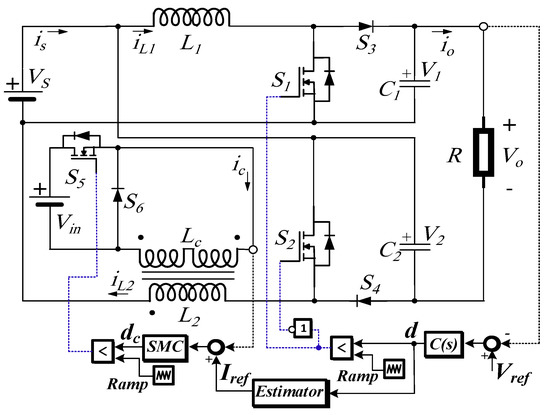
Figure 1.
Schematic diagram of FIBC with a VI and its control structure.
This paper is organized as follows. In Section 2, the operation and analysis are conducted, including the voltage gain, dynamic modeling, and control of the main converter. Section 3 introduces the operation principle and design method for the VI. The equivalent model of the VI and proposed controller with a reference current estimator are provided in Section 4. Experimental results and the corresponding analysis are described in Section 5. Finally, the paper is concluded in Section 6.
2. Main Converter Analysis
The FIBC is shown in Figure 2a. This converter is applied in FC and PV applications to reduce the current and voltage stress in the switching devices, which substantially increases the overall efficiency of the system by reducing the ICR [19].
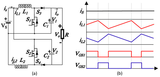
Figure 2.
Two-phase FIBC when = 0.7 and = 0.3: (a) schematic diagram; (b) relevant waveforms.
To increase the voltage gain, a duty cycle different from 0.5 is required. The switches and operate inversely to minimize the ICR owing to the summation of the currents through each inductor. In this case, the phases present opposite slopes and complementary duty cycles, as shown in Figure 2b.
2.1. Steady State Analysis
The elimination of the ICR is achieved by matching the current ripple in the inductors, which can be mathematically expressed using the equation:
where is the switching frequency, is the duty cycle for the converter, and are the inductances, and is the source voltage. After some elementary algebraic transformations, Equation (1) yields:
It follows immediately from (2) that, in order to compensate for the change in the duty cycle , the inductance () must be a variable one. According to Kirchhoff’s voltage law, the output voltage is given as:
hence, the static gain of the converter is:
Denoting , and assuming that ICR is completely mitigated, one obtains from (3) the value of the duty cycle:
The voltage gain of Equation (4) for different values of is shown in Figure 3.
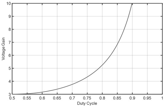
Figure 3.
Voltage gain of FIBC for different values of .
2.2. The Dynamic Model of FIBC
According to the model presented in [9] with complementary duty cycles, under continuous conduction mode, the averaged model of the converter is:
where the state variable represents the average inductor current (), represents the average capacitor voltage (), represents the average inductor current (), and represents the average capacitor voltage (). The components , , , , and represent the inductors, capacitors, and load resistor, respectively.
Setting to zero, the relevant derivatives in (6) yields:
from Equation (7), one may obtain the equilibrium point.
From Equation (6), the linearization of the average model, around the desired equilibrium point , yields the following state equations:
with , , , , , and , where the superscript (~) represents the linearized signal. The system matrix is given by:
While the input matrix is given by:
In the case of the output matrix:
The matrix transfer function corresponding to the state Equation (8) is:
Expression (12) can be developed into
where the numerator coefficients of Equation (13) are:
and the denominator coefficients of Equation (13) are:
2.3. Output Voltage Control
In this system, it is possible to control both capacitor voltages with only one controller. The different dynamic transfer functions from (13) are added to obtain the relation between the input and output . Considering as a perturbation, this yields:
where , , and .
The inductance variation of produces an interval plant and is considered for controller design, with as a minimum inductance and as a maximum inductance. Expression (14) is defined as a set of transfer functions achieved using:
and coefficients are supposed to vary within the following bounds:
where represents the minimum numerator coefficient, represents the maximum numerator coefficient, represents the minimum denominator coefficient, and represents the maximum denominator coefficient.
A first-order controller is needed with an acceptable range, which robustly stabilizes the trajectories of the closed-loop system, under parameter variations, around a region defined by the interval plant. The output voltage controller is chosen as a proportional-integral controller as follows:
where is the proportional gain and is the integral gain.
The characteristic equation for a closed-loop system is expressed as follows:
Using (18), the transfer function (15) is evaluated with a uniform distribution of interval . The stability of these polynomials can be tested via Routh–Hurwitz test. The stability condition must be fulfilled for all transfer functions—in this case, the number selected is ten. This proof generates an area of the acceptable range of controller parameters that robustly stabilize the interval plant, as depicted in Figure 4.
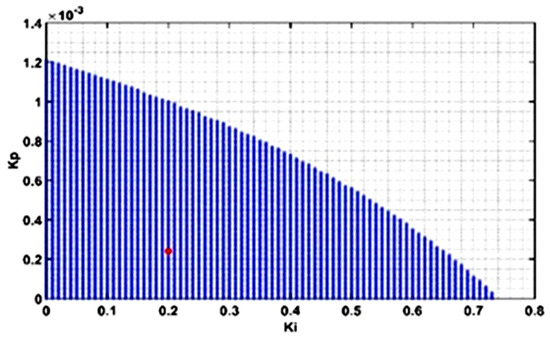
Figure 4.
Acceptable proportional and integral gains; the red dot represents the selected controller parameters.
The closed-loop Bode diagram for the linear control system of the plant model (15) with the controller designed is shown in Figure 5. The crossover frequency is 561 Hz. The phase margin is ranged from 37.6° to 40.1° and the gain margin ranged from 7.73 dB to 9.11 dB.
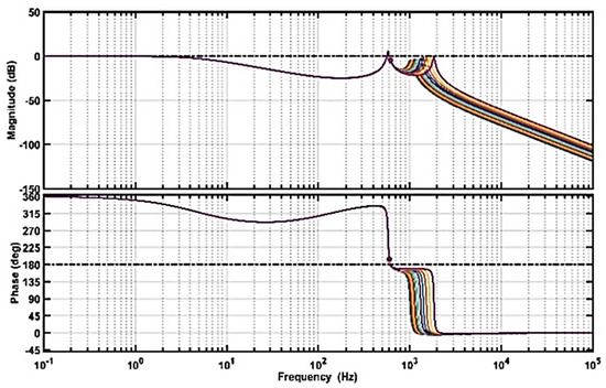
Figure 5.
Bode diagram of closed-loop transfer functions for uniform distributed parameter .
3. Variable Inductor Operation and Design
The VI based on a double E-core contains a control winding and the main winding. The principle of operation is based on the variation of the main winding inductance through the control of the flux created by the control winding. The reluctance model and design algorithms have been reported in the literature [20,21].
Figure 6a shows a schematic representation of the windings for practical implementation. Figure 6b illustrates the operating points on the B–H curve.
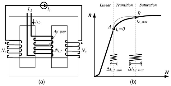
Figure 6.
Complete VI model: (a) winding distribution; (b) operating points on B–H curve.
The reluctance model depicted in Figure 7 is required to determine the appropriate characteristics and paths of VI.
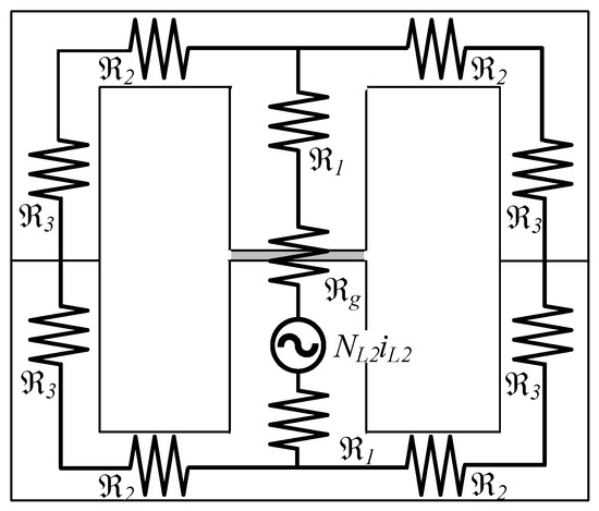
Figure 7.
Reluctance model of VI.
The inductance will vary between points A and B, according to Figure 5. Point A starts after the linear region; point B reaches the value before the core saturation. Point A has the minimum current ripple when ΔiL2 = ΔiL2_min, having a control current ic = 0; thus, the main inductance is maximum L2 = Lmax.
The maximum inductance can be obtained with [21]:
where , , , and are the equivalent reluctances values of the gap, center arm, left arm, and right arm, respectively, and is the main winding number of turns.
The final state reaches point B when the current ripple is maximum ΔiL2 = ΔiL2_max, and the current is maximum ic = ic_max; therefore, the main inductance is minimum L2 = Lmin. Control winding creates a magnetic saturation along the flux path of the left and right arms. Then, the reluctance and must be replaced with and . The length of the saturated area in the core is associated with the values provided by the manufacturer, as shown in Figure 8.
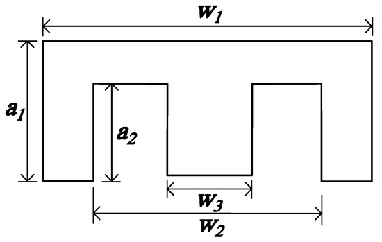
Figure 8.
Dimensions of magnetic E-core for modified reluctance calculation.
The calculation of the equivalent reluctance for the saturated condition is necessary to determine the length of the saturated region, as follows [21]:
where and are the length values provided by the manufacturer. The equivalent reluctance for saturation condition and can be calculated as:
where is the length of the magnetic path , is the value of the differential permeability for the saturation condition, and is the cross-section of the path. The properties of the magnetic materials are illustrated in B–H curves, where the permeability for each reluctance is obtained; then, the equations are achieved using:
Equation (23) is the slope of the linear region, which is required to estimate the reluctance in (19). Considering (20)–(24), the minimum inductance can be obtained as:
Flux density must be limited to guarantee that the VI does not operate in the saturation region. Thus, the following condition must be fulfilled [22]:
From (26), the maximum peak current iL2_max can be calculated as:
where is the denominator of (19), is the cross-section of the center arm, and is the saturation flux density. If Equation (27) cannot be fulfilled, a bigger core must be selected. Furthermore, the control winding number of turns is achieved using:
where is the saturation magnetic field and and are the magnetic paths of the right arm and left arm, respectively.
4. Current Controller and Reference Estimator
4.1. Current Controller for VI
The VI, in general, suffers from two main uncertainties. The first is the parameter variations, where the inductance changes due to the current of the main converter and auxiliary SCC. The temperature effect is the second important source of uncertainty and is typically unknown.
The dynamic model of VI with uncertainties is written as:
where , , and are the control current, inductance, and resistance of the control inductor, respectively, is the perturbation term that contains parameter variations and external disturbances, is the voltage input of switching current-source converter, and is the control input.
The perturbation term is unknown but bounded. Moreover, consider that satisfies the matching condition [23], that is:
From (29) and (30), the dynamic model of VI can be expressed as follows:
The norm of perturbation term is calculated considering a Lipschitz condition, that is:
A sliding mode controller (SMC) via fixed-frequency is proposed to add robustness under uncertainties. Considering as the current reference, a sliding surface can be written as:
In order to drive the sliding surface (33) to zero, the following reaching law is proposed:
Substituting the time derivative of (33) into (34) to stabilize the system (31) and regulate the current , the control input is selected as:
Under the condition , Equation (34) is negative and the surface (33) converges to zero in a finite time [23].
4.2. Reference Estimator
The current reference estimator is determined from a series of tests. For several average current levels of in the main winding, the control current is varied in steps of 5 mA until a minimum ICR in is noticed for each duty cycle. The effect of on inductance is not significant for this converter since the current variation of the variable inductor phase is less than 500 mA.
Figure 9 demonstrates the characteristics of the inductance curve as a function of the DC control current. As can be observed, the inductance value is inversely proportional to the control current.
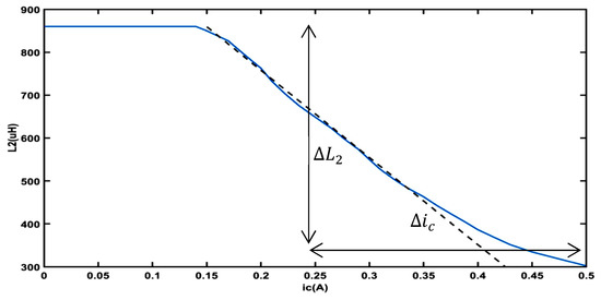
Figure 9.
Characteristic inductance curve.
A linear approximation can be used to relate the control current and inductance over a specified span as follows:
where is the change in the value of , is the change in the value of , and is the minimum control current. Considering Equation (2), when with as the reference current, that is:
5. Experimental Results
A prototype of FIBC and VI was implemented to validate the proposed zero-ripple input current method (Figure 10). The specifications of the prototype are shown in Table 1. The controllers were implemented using a CompactRIO embedded system with an NI cRIO-9067 chassis, NI 9223 analog input module, and NI 9401 digital output module.
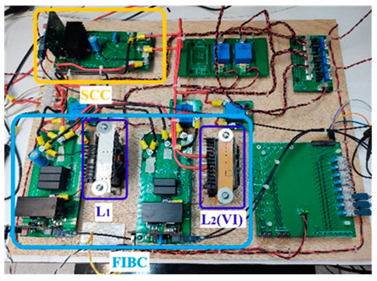
Figure 10.
Experimental prototype.

Table 1.
Specifications of the prototype.
The VI was implemented in an ETD 59/31/22 E-core with 3C90 magnetic material, = 43, = 185. A first test was performed to measure the control inductance using a Hewlett Packard 4263B LCR meter. In this case, the main current = 0, for which presents an average value of 120 mH and ESR of 3.2 Ω. The current controller was set up and incorporated these parameters and the controller gain = 15.
Once the VI controller was finished, the test was carried out with the main converter in an open/closed loop. Two tests are made in an open loop: 300 Ω constant output load and 150 V constant output voltage . In the case of a closed loop, two types of tests are made: change of load from half load to full load and change of input voltage .
5.1. Main Converter Open-Loop Test
Figure 11 shows the current of inductors in the traditional duty cycle = 0.5 for two-phase interleaved converters when the output load was 300 Ω and zero-ripple input current occurs naturally. It can be observed that the current ripple of the VI is distorted due to many reasons: the core is forced to operate within the limits of the linear and transitions regions when = 0, but also within the unbalance of the winding arms, which has an impact on the magnetic reluctance and parasites and the parasitic capacitance of the windings in high frequency [24]. A small film capacitor can be added to remove the residual ICR in the case of L_1 parameter deviation.
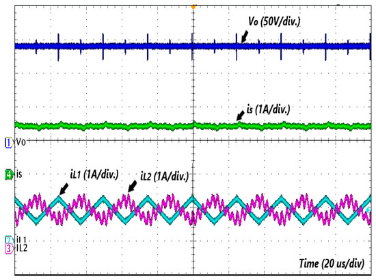
Figure 11.
Traditional duty cycle = 0.5.
In Figure 12a, the duty cycle is set to d = 0.7; the ICR presents a deviation compared to the operation with d = 0.5. There is a high ICR, in this case, since the inductances are different. The average currents of the inductors are i_L1 = 2 A and i_L2 = 1 A, and the current ripple distortion is maintained.
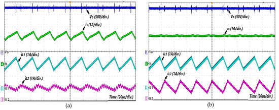
Figure 12.
Waveforms of currents/voltage of open loop tests: (a) ICR presence at = 0.7; (b) zero-ripple input current at = 0.7.
Figure 12b shows that the ICR for both inductors are now different; however, the current ripple with the same magnitude, and then a zero-ripple input current, occurs with the corresponding control current ( = 395 mA). The signal waveform behavior depicted in Figure 2 is therefore confirmed. The current ripple distortion is slightly noticeable, and the duty cycle is kept.
The transient state waveform of the VI current ripple is shown in Figure 13. The control current of the inductor is changed from 0 to 395 mA. The ICR changes from = 0.7 A to zero-ripple, and the transient response is about 8 ms with asymptotic behavior. This characteristic behavior is required with the closed-loop main converter when this variation represents a negligible disturbance. As observed, the inductor current and output voltage are not affected by increased . Larger the value of the faster the trajectory converges to the sliding surface. The closed-loop response of VI should be faster than the transient response of the main converter to guarantee stability.
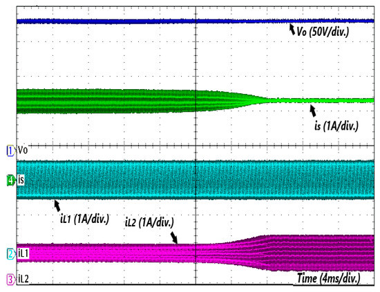
Figure 13.
Ripple current in a steady state.
A comparison of the measured efficiency with different output powers is depicted in Figure 14. The efficiency values presented were all measured using the Chroma 62204 power meter, 48 V nominal input voltage , and 150 V nominal output voltage . The converter efficiency with the zero-ripple input current presents a similar trajectory with a maximum difference of 0.92 %, including the VI power consumption. The efficiency of the proposed converter-rated power is 94.47%, which is 0.24% less than conventional. The maximum control current in this test is = 280 mA at 50 W. The efficiency decrease is due to power losses in the SCC and conduction loss in the auxiliary winding of the VI. Knowledge of these power losses is necessary to evaluate the conversion efficiency of the system. The losses of the inductor and the diodes strongly influence the total efficiency of the converter. The effect of the capacitor series resistance is negligible for the voltage gain factor. The efficiency of the phases is expected to be different compared to the conventional FIBC.
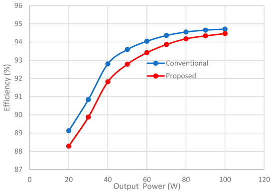
Figure 14.
Efficiency comparison.
5.2. Main Converter Closed-Loop Test
The dynamic response of FIBC under the action of a robust PI controller is shown in Figure 15 when the output load is changed from half load to full load and the reference voltage is 150 V. As can be observed, variation in the inductance parameter value does not cause a significant change in performance or stability. Additionally, according to the load step test, one can conclude that the zero-ripple input current in the transient response is maintained. The settling time is about 2 ms, which is a good response for boosting converters with high gain, and the voltage overshoot is 8 V.
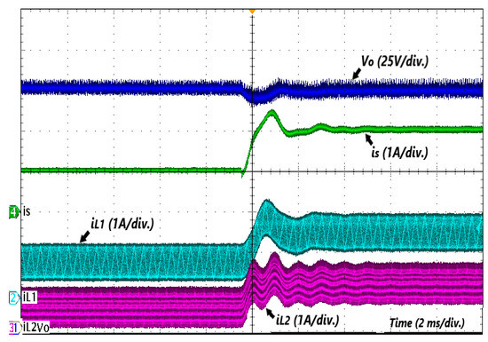
Figure 15.
Transient response under load changes.
The controller is tested under input voltage change from 48 V to 43 V and vice versa (Figure 16). A fast dynamic response is observed, and the zero-current ripple is maintained all the time, even at different operating points, which is the main advantage of the proposal. The dynamic response is about 60 ms, and the voltage overshoot and voltage drop are within 13 V. In summary, the dynamic experiment shows that the proposed converter has strong robustness under the PI control strategy, which is beneficial to ensure the stable output of the power source.
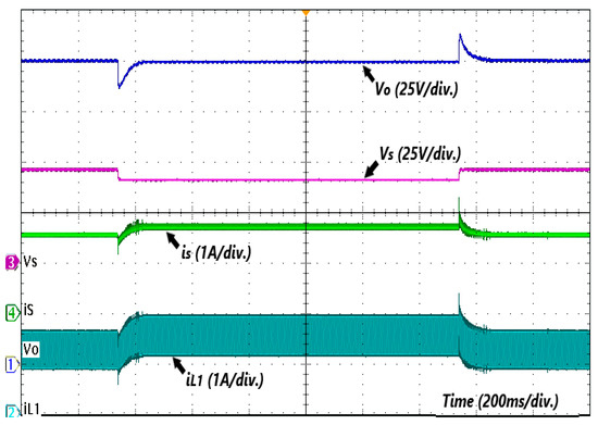
Figure 16.
Transient response under input voltage change.
6. Conclusions
In this paper, a zero-ripple input current FIBC using a VI has been introduced. The inductance variation is fast and its effect is reflected in the main converter as a negligible disturbance. The converter presents a wide operating region without affecting the zero-ripple condition. The interval plant model stability is verified via Routh–Hurwitz. The PI controller is designed under parameter variation of inductance. The dynamical behavior of the converter permits the use of only one voltage controller. Only one magnetic component is used to achieve the power transfer and zero-ripple. The main converter and the SCC are galvanically isolated. Different voltage supplies can be used for the current regulation of the VI. A dynamic model has been developed which describes the behavior of a VI, including uncertainties. Experimental results of the proposed SCC revealed that a simple current control loop is employed to adjust the inductance, and that the efficiency of the main converter is not significantly decreased. Operating at the rated 100 W power, the proposed converter achieved 94.47% efficiency. The current controller offers remarkable accuracy, robustness, low computational load, and easy tuning for implementation. The proposed reference estimator determines the amount of auxiliary winding current based on the main duty cycle levels. The introduced converter is suitable for renewable sources where a lower ripple is demanded. Future research will focus on the experimental validation of the proposed estimator with a large-scale VI-based DC–DC converter with variable load.
Author Contributions
Conceptualization, H.H. and N.V.; Investigation, H.H.; Methodology, N.V. and H.H.; Supervision, N.V., R.O., H.H.-Á. and S.P.; Writing—original draft, H.H.; Writing—review and editing, N.V., S.P. and L.E. All authors have read and agreed to the published version of the manuscript.
Funding
This work was sponsored by TecNM.
Data Availability Statement
Data is contained in the paper.
Conflicts of Interest
The authors declare no conflict of interest.
References
- Elkhateb, A.; Rahim, N.A.; Selvaraj, J.; Williams, B.W. DC-to-DC Converter With Low Input Current Ripple for Maximum Photovoltaic Power Extraction. IEEE Trans. Ind. Electron. 2015, 62, 2246–2256. [Google Scholar] [CrossRef]
- Lu, N.; Yang, S.; Tang, Y. Ripple Current Reduction for Fuel-Cell-Powered Single-Phase Uninterruptible Power Supplies. IEEE Trans. Ind. Electron. 2017, 64, 6607–6617. [Google Scholar] [CrossRef]
- Gu, Y.; Zhang, D.; Zhao, Z. Input/Output Current Ripple Cancellation and RHP Zero Elimination in a Boost Converter Using an Integrated Magnetic Technique. IEEE Trans. Power Electron. 2015, 30, 747–756. [Google Scholar] [CrossRef]
- Gu, Y.; Zhang, D.; Zhao, Z. Input Current Ripple Cancellation Technique for Boost Converter Using Tapped Inductor. IEEE Trans. Ind. Electron. 2014, 61, 5323–5333. [Google Scholar] [CrossRef]
- Nandankar, P.; Rothe, J.P. Design and Implementation of Efficient Three-Phase Interleaved DC-DC Converter. In Proceedings of the 2016 International Conference on Electrical, Electronics, and Optimization Techniques (ICEEOT), Mumbai, India, 26–27 February 2016; pp. 1632–1637. [Google Scholar]
- Joo, D.-M.; Kim, D.-H.; Lee, B.-K. DCM Frequency Control Algorithm for Multi-Phase DC-DC Boost Converters for Input Current Ripple Reduction. J. Electr. Eng. Technol. 2015, 10, 2307–2314. [Google Scholar] [CrossRef]
- Antares, B.; Makarim, F.H.; Ilman, S.M.; Rizqiawan, A.; Dahono, P.A. Analysis and Control of Cascade Multiphase DC-DC Boost Converters with Very Low Input Current Ripple. In Proceedings of the 2019 2nd International Conference on High Voltage Engineering and Power Systems (ICHVEPS), Denpasar, Indonesia, 1–4 October 2019; pp. 1–6. [Google Scholar]
- Huangfu, Y.; Zhuo, S.; Chen, F.; Pang, S.; Zhao, D.; Gao, F. Robust Voltage Control of Floating Interleaved Boost Converter for Fuel Cell Systems. IEEE Trans. Ind. Appl. 2018, 54, 665–674. [Google Scholar] [CrossRef]
- Villarreal-Hernandez, C.A.; Mayo-Maldonado, J.C.; Escobar, G.; Loranca-Coutino, J.; Valdez-Resendiz, J.E.; Rosas-Caro, J.C. Discrete-Time Modeling and Control of Double Dual Boost Converters With Implicit Current Ripple Cancellation Over a Wide Operating Range. IEEE Trans. Ind. Electron. 2021, 68, 5966–5977. [Google Scholar] [CrossRef]
- Beraki, M.; Perdigao, M.; Machado, F.; Trovao, J.P. Auxiliary Converter for Variable Inductor Control in a DC-DC Converter Application. In Proceedings of the 2016 51st International Universities Power Engineering Conference (UPEC), Coimbra, Portugal, 6–9 September 2016; pp. 1–6. [Google Scholar]
- Beraki, M.W.; Trovao, J.P.F.; Perdigao, M.S.; Dubois, M.R. Variable Inductor Based Bidirectional DC–DC Converter for Electric Vehicles. IEEE Trans. Veh. Technol. 2017, 66, 8764–8772. [Google Scholar] [CrossRef]
- Beraki, M.; Trovao, J.P.; Perdigao, M. Design of Variable Inductor for Powertrain DC-DC Converter. In Proceedings of the 2019 IEEE 28th International Symposium on Industrial Electronics (ISIE), Vancouver, BC, Canada, 12–14 June 2019; pp. 822–827. [Google Scholar]
- Wei, Y.; Luo, Q.; Du, X.; Altin, N.; Alonso, J.M.; Mantooth, H.A. Analysis and Design of the LLC Resonant Converter With Variable Inductor Control Based on Time-Domain Analysis. IEEE Trans. Ind. Electron. 2020, 67, 5432–5443. [Google Scholar] [CrossRef]
- Babaiahgari, B.; Jeong, Y.; Park, J.-D. Stability Enhancement Method for DC Microgrids with Constant Power Loads Using Variable Inductor. In Proceedings of the 2020 IEEE Applied Power Electronics Conference and Exposition (APEC), New Orleans, LA, USA, 15–19 March 2020; pp. 2236–2240. [Google Scholar]
- Mendes, A.P.; Baptista, B.; Perdigao, M.S.; Mendes, A.M.S. Experimental Analysis of a DC Current-Controlled Variable Inductor in a DC-DC Converter. In Proceedings of the 2019 IEEE International Conference on Industrial Technology (ICIT), Melbourne, Australia, 13–15 February 2019; pp. 440–445. [Google Scholar]
- Alonso, J.M.; Perdigao, M.S.; Abdelmessih, G.Z.; Dalla Costa, M.A.; Wang, Y. SPICE Modeling of Variable Inductors and Its Application to Single Inductor LED Driver Design. IEEE Trans. Ind. Electron. 2017, 64, 5894–5903. [Google Scholar] [CrossRef]
- Chinchero, H.; Alonso, M. Using Magnetic Control of DC-DC Converters in LED Driver Applications. IEEE Lat. Am. Trans. 2021, 19, 297–305. [Google Scholar] [CrossRef]
- Yao, K.; Zhang, Z.; Yang, J.; Liu, J.; Li, J.; Shao, F. Quasi-Fixed Switching Frequency Control of CRM Boost PFC Converter Based on Variable Inductor in Wide Input Voltage Range. IEEE Trans. Power Electron. 2021, 36, 1814–1827. [Google Scholar] [CrossRef]
- Zhuo, S.; Gaillard, A.; Paire, D.; Breaz, E.; Gao, F. Design and Control of a Floating Interleaved Boost DC-DC Converter for Fuel Cell Applications. In Proceedings of the IECON 2018—44th Annual Conference of the IEEE Industrial Electronics Society, Washington, DC, USA, 21–23 October 2018; pp. 2026–2031. [Google Scholar]
- Alonso, J.M.; Perdigao, M.; Dalla Costa, M.A.; Zhang, S.; Wang, Y. Variable Inductor Modeling Revisited: The Analytical Approach. In Proceedings of the 2017 IEEE Energy Conversion Congress and Exposition (ECCE), Cincinnati, OH, USA, 1–5 October 2017; pp. 895–902. [Google Scholar]
- Saeed, S.; Garcia, J.; Perdigao, M.S.; Costa, V.S.; Baptista, B.; Mendes, A.M.S. Improved Inductance Calculation in Variable Power Inductors by Adjustment of the Reluctance Model Through Magnetic Path Analysis. IEEE Trans. Ind. Appl. 2021, 57, 1572–1587. [Google Scholar] [CrossRef]
- Ferreira, S.F.S. Electromagnetic Study of a Variable Inductor Controlled by a DC Current. Master’s Thesis, Universidade de Coimbra, Coimbra, Portugal, 2016. [Google Scholar]
- Utkin, V.; Guldner, J.; Shi, J. Sliding Mode Control in Electro-Mechanical Systems; CRC Press: Boca Raton, FL, USA, 2017; ISBN 9781315218977. [Google Scholar]
- Saeed, S.; Georgious, R.; Garcia, J. Modeling of Magnetic Elements Including Losses—Application to Variable Inductor. Energies 2020, 13, 1865. [Google Scholar] [CrossRef]
Disclaimer/Publisher’s Note: The statements, opinions and data contained in all publications are solely those of the individual author(s) and contributor(s) and not of MDPI and/or the editor(s). MDPI and/or the editor(s) disclaim responsibility for any injury to people or property resulting from any ideas, methods, instructions or products referred to in the content. |
© 2023 by the authors. Licensee MDPI, Basel, Switzerland. This article is an open access article distributed under the terms and conditions of the Creative Commons Attribution (CC BY) license (https://creativecommons.org/licenses/by/4.0/).