Abstract
This paper presents the analysis and design of the harmonic rejection (HR) low-noise amplifier (LNA) with the fully passive source degeneration notch filter. The proposed HR LNA provides the rejection for the strong harmonics () of the local oscillator (LO) frequencies, where the HR mixer does not provide sufficient HR performance. The proposed harmonic notch filter modulates the source degeneration factor and the impedance matching performance thereafter. This effect further helps the blocking of the harmonic signal. The proposed LNA provides 11 dB gain at the fundamental frequency (2.1 GHz) while rejecting the 3rd harmonic component by 37 dBc. Compared to the conventional LNA, the 3rd harmonic notch performance is improved by 23 dB. Additionally, the LNA achieves a minimum noise figure of 3.1 dB, third order input intercept point () of 0.5 dBm, input reflection (S) below −10 dB from 1.8 GHz–2.3 GHz operational frequency range, and consumed 19 mW of power from a 1.2 V supply.
1. Introduction
The switching mixer down-converts the harmonics of the local oscillator (LO) signal and corrupts the desired signal in RF receivers. The de-sensitization due to the harmonics is not the exception for the narrow-band receivers. In the architecture of a radio-frequency (RF) receiver, the frequency conversion circuit, also known as a down-conversion mixer, is used to shift the desired RF channel signal to either the base-band or intermediate-frequency (IF). A frequency translation can be achieved by breaking the linear time-invariant (LTI) property and the linear time-varying switching mixer is the norm for modern RF receivers due to its superior performance in terms of the conversion gain and noise figure [1,2,3].
The switching mixer, on the other hand, is notorious for harmonic spurious issue, where the square-wave-like local oscillator LO signal down-converts the interferences at the harmonics of the LO fundamental frequency () [4]. This harmonic alias is a serious problem for broadband radio, where the larger blockers are passed upon the receiver without any pre-filtering (attenuation) and thus harmonic rejection (HR) mixer has to be used, albeit with a circuit complexity and an in-sufficient HR performance [5,6].
An HR issue is considered irrelevant for narrowband radio along with the off-chip filtering components. However, recent trends favor the wide-band analog front-end in order to cover vastly different frequency bands and to lower the cost of the RF transceiver, especially in Long Term Evolution (LTE) [7]. Thus, blocker signals may reach the HR mixer where the harmonic alias rejection is usually in the range of 40–50 dBc only [5,6,8].
We propose the HR LNA with a source degeneration notch filter embedded within the amplifying stage. The novelty of the proposed HR LNA is due to features which include: (1) the harmonic filtering occurs before the current to voltage conversion in the load of the LNA and thus the desensitization due to the strong blockers is prevented in the first stage of the receiver chain; (2) the harmonic rejection requirement on the HR mixer is significantly relaxed with the help of HR LNA; (3) the proposed source degeneration notch filter is fully passive and incurs no additional current consumption, and; (4) the source degeneration factor is modulated for the rejection of harmonic and the blockers around of the LNA is reflected across the antenna-LNA interface.
2. Proposed Notch LNA
Figure 1 shows the proposed LNA architecture which is based on the inductor degenerated LNA architecture [9]. Instead of the inductor degeneration, the proposed LNA has the LC resonator as the degeneration component, where the desired resonance is at . The degeneration capacitor is employed to form a parallel LC notch filter at the to provide the required filtering of the third harmonic components.
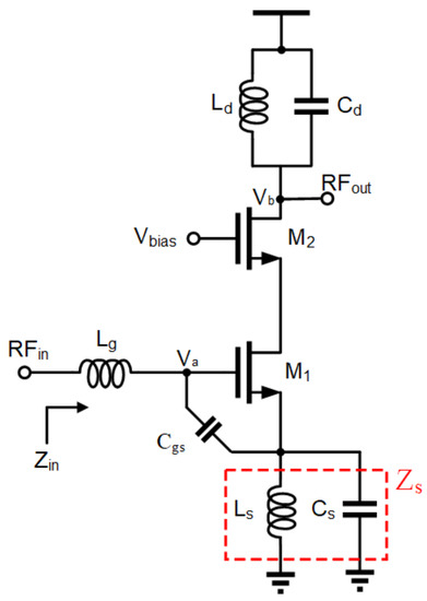
Figure 1.
Schematic diagram of the proposed LNA with the notch filter.
The impedance () of the LC resonator with finite quality factor () of the inductor is expressed as [10]
where is the series resistance due to the finite of the inductor and is located at harmonic frequency (). Then, the effective input impedance () exhibits two distinct characteristics at the desired operating frequency range () and undesired harmonic frequency range ().
With as the trans-conductance of , can be expressed as
In addition, Equation (3) manifests the large real impedance () at , thereby the undesired signals around are severely unmatched regardless of the exact resonance frequency at
The proposed LNA with a source degeneration notch filter is advantageous for the gain at the fundamental frequency . The effective trans-conductance of the proposed circuit before the current to voltage conversion in the load can be expressed as follows.
where Q(s) is the effective quality factor of the input impedance and depends on the operating frequency ranges as depicted below [4].
Equations (8) and (9) are calculated based on the frequency-dependent source degeneration impedance, whose impedance (Z(s)) behaves as an inductor and a resistor at the fundamental and 3rd harmonic frequencies. R is the impedance seen into the direction of antenna (usually 50 ohms). From the simulation, Q() and Q(3) are obtained to be 4.74 and 0.18 respectively. Then, G recorded a boosting factor of 4.74 at .
The output impedance of the proposed LNA at is , where Q and R refers to the quality factor and the series parasitic resistance of the inductor load, L. Then, stand-alone LNA requires the output buffer, whose impedance is ideally matched to the measurement port (=50 ). Figure 2 shows the schematic of the source follower circuit, from the figure, the transistors M and M constitute the main trans-conductor and the current bias respectively. Neglecting the body effect, the output impedance of the source follower buffer is given by
where g is the transconductance of the source trans-conductor (M).
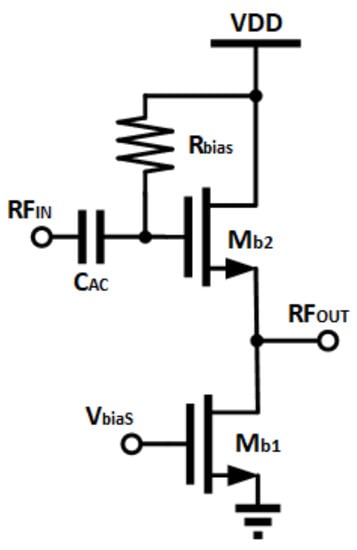
Figure 2.
Schematic of the source follower output buffer.
Table 1 lists the device used in the LNA and output buffer. The design procedure of the harmonic rejection LNA is as follows. We choose the optimum quality factor of the input impedance at , which is also the function of (and device width of main trans-conducting transistor, ). The current consumption of the amplifier is dictated by the power budget. In our design, the proposed LNA consumed 15.8 mA and subsequently we could determine the dc bias, trans-conductance of , and the overdrive voltage of . Required real impedance of 50 along with the resonance at dictates the inductance at the source and the gate. The capacitor at the source has the desired harmonic resonance at 3 and thus we could easily determine the required capacitor size given the inductance (). The transistor as the cascoded device as well as the load resonator (, ) are carefully designed while optimizing the current transfer due to and maximizing the load impedance at .

Table 1.
Device Dimension.
3. Verifications
The proposed LNA was implemented with TSMC 40 nm CMOS technology and verified with Cadence Virtuoso. The final layout of the proposed LNA with an embedded notch filter is shown in Figure 3.
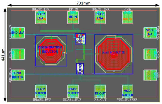
Figure 3.
Layout photograph of the proposed LNA.
Due to the large value of the gate inductor (L) required, it is placed off-chip, providing much higher quality factor than the on-chip realization. A total area of 0.441 mm × 0.731 mm including the pad was achieved. An important compromise was made between lower metal layers and higher metal layers to avoid too much parasitic capacitance effect which leads to frequency shift and gain reduction. The lower metals are used in the layout of the LNA core to minimize parasitic capacitance effect. The LC resonators are positioned relatively far from each other and also the active devices, hence the need to employ high metal layers to minimize series resistance on the connecting metals.
The frequency response of is shown in Figure 4. The LNA exhibits a real impedance of about 50 around the fundamental frequency while presenting extremely high impedance at as presented in Equation (3). At , the effective resistance is a function of the antenna resistance and the square of the effective quality factor.
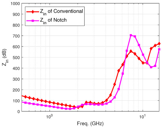
Figure 4.
Input impedance (Z) of the proposed notch LNA compared to the conventional LNA.
Figure 5 shows the power gain of the proposed LNA compared to the conventional LNA without the notch filter. The cut-off frequency of the band-pass filter employed at the load is carefully tuned to occur around 3. The LC resonator’s reactance increases extremely near the cut-off frequency resulting in a gain reduction of about 14 dBc without the notch filter. With the addition of the notch filter, the attenuation is further improved at 3 by 23 dBc. The gain difference for the conventional and the proposed embedded notch filter LNA is only 1.5 dB at the fundamental frequency (2.1 GHz).
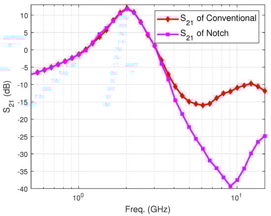
Figure 5.
Gain performance of the proposed notch LNA compared to the conventional LNA.
Figure 6 shows the input reflection of the conventional versus the proposed LNA. The input reflection (S) is below −10 dB for a frequency range of 1.9 GHz–2.5 GHz without the notch filter. However, S with the notch filter has a frequency range of 1.8 GHz–2.3 GHz. It clearly shows a slight frequency shift, which is as a result of the degeneration capacitor (C) and other undesired parasitic effects resulting from the layout.
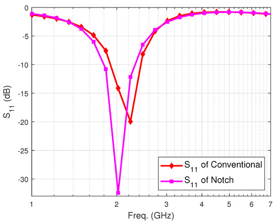
Figure 6.
Input reflection (S) performance of the proposed notch LNA compared to the conventional LNA.
The large signal noise figure performance of the proposed LNA is depicted in Figure 7. The large blocker tone at 3 (=6.3 GHz) is imposed on the LNA input while its power is varied from −10 dBm to 30 dBm. The proposed LNA exhibits 0.2 dB higher NF compared to the conventional LNA. On the other hand, the benefit due to the proposed notch LNA is evident from the large-signal NF results with >15 dBm blocker level.
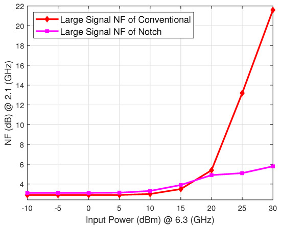
Figure 7.
Large signal noise figure performance of the proposed notch LNA compared to the conventional LNA.
The source follower buffer with an output impedance of is designed to achieve an output reflection of less than −20 dB as shown in Figure 8.
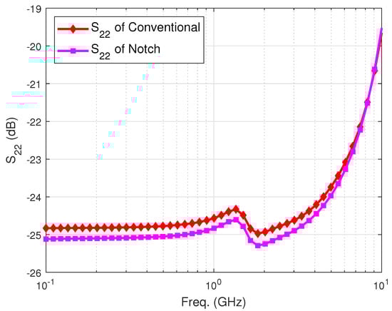
Figure 8.
Output reflection (S) performance of the proposed notch LNA compared to the conventional LNA.
The LNA also demonstrated a very good input third-order intercept point (IIP) performance of about 0.5 dBm as shown in Figure 9.
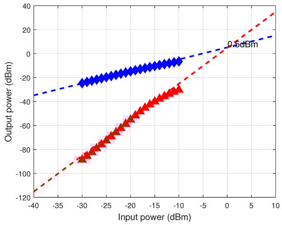
Figure 9.
Input third-order intercept point (IIP).
Table 2 gives the power at the gate of the input transistor and that of the drain of the cascode transistor when fed with an input signal tone of −50 dBm. The power gain/attenuation is obtained by assigning output ports at nodes V and V shown in the schematic of Figure 1. The gain/attenuation is observed at both the fundamental and third harmonic frequencies which are very close to that of the S parameter for the conventional as well as the notch LNA.
Table 2.
Performance Comparison of Conventional versus Proposed Notch LNAs, [input power = −50 dBm].
A comparison of this work with other related works is given in Table 3. Some of the works in (Table 3) did not provide explicit performance for the harmonic rejection and thus are estimated from the gain (S) performance. Our work demonstrated the best harmonic rejection performance with a superior noise figure and better linearity.
Table 3.
Performance Comparison.
4. Conclusions
In this paper, the harmonic rejection LNA with an embedded notch filter as the source degeneration component is proposed to enhance the filtering of 3 harmonic signals in an RF receiver system. The frequency-dependent source degeneration impedance, the LNA input impedance, as well as the signal gain/attenuation at both the fundamental and 3 harmonic frequencies of the notch filter are analyzed, and the various equations give an accurate relation with that of the simulated results. The simulation results verify that the proposed LNA can attenuate third harmonic signals by 37 dBc while providing a sufficient gain of 11 dB at the fundamental frequency. The LNA demonstrated the noise figure of 3.1 dB with a large blocker tone of 5 dBm at 3 imposed upon the LNA input.
Author Contributions
Conceptualization, R.G.; validation, R.G.; formal analysis, R.G. and D.-H.L.; writing, R.G. and J.K.; supervision, D.-H.L. and J.K. All authors have read and agreed to the published version of the manuscript.
Funding
This work was supported by the National Research Foundation of Korea (NRF) grant funded by the Korea Government (MSIP) (No. NRF-2019R1F1A1048784).
Acknowledgments
The EDA tool was supported by the IC Design Education Center (IDEC), Korea.
Conflicts of Interest
The authors declare no conflict of interest.
References
- Kim, J.; Silva-Martinez, J. Low-power, low-cost CMOS direct-conversion receiver front-end for multi-standard applications. IEEE J. Solid-State Circuits. 2013, 48, 2090–2103. [Google Scholar]
- Kulkarni, R.; Kim, J.; Jeon, H.-J.; Xiao, J.; Silva-Martinez, J. UHF receiver front-end: Implementation and analog baseband design considerations. IEEE Trans. Very Large Scale Integr. (Vlsi) Syst. 2013, 20, 197–210. [Google Scholar] [CrossRef]
- Kim, J. Broadband RF Front-End Design for Multi-Standard Receiver with High-Linearity and Low-Noise Techniques. Ph.D. Thesis, Texas A&M University, College Station, TX, USA, 2012. [Google Scholar]
- Behzad, R. RF Microelectronics, 2nd ed.; Prentice Hall: Upper Saddle River, NJ, USA, 1998; pp. 63–70. [Google Scholar]
- Aslam, A.R.; Alessandro, P.; Peter, V.; Tyson, T. A harmonic rejection mixer robust to RF device mismatches. In Proceedings of the International Solid-State Circuit Conference, San Francisco, CA, USA, 20–24 February 2011; pp. 66–67. [Google Scholar]
- Ru, Z.; Klumperink, E.A.M.; Wienk, G.J.M.; Nauta, B. A software-defined radio receiver architecture robust to out-of-band interference. In Proceedings of the International Solid-State Circuit Conference, San Francisco, CA, USA, 8–12 February 2009; pp. 230–231. [Google Scholar]
- Andreas, G.; Silvester, S.; Stefan, T.; Krzysztof, D.; Harald, P.; Mario, H. A harmonic rejection strategy for 25% Duty-Cycle IQ-mixers using digital-to-time converters. In IEEE Transactions on Circuits and Systems II: Express Briefs (Early Access); IEEE: Piscataway, NJ, USA, 2019. [Google Scholar] [CrossRef]
- Cha, H.-K.; Kwon, K.; Choi, J.; Kim, H.-T.; Lee, K. A CMOS wideband RF front-end with mismatch calibrated harmonic rejection mixer for terrestrial digital TV tuner applications. IEEE Trans. Microw. Theory Tech. 2010, 58, 2143–2151. [Google Scholar] [CrossRef]
- Shaeffer, D.K.; Lee, T.H. A 1.5-V, 1.5-GHz CMOS low noise amplifier. IEEE J. Solid-State Circuits 1997, 32, 745–759. [Google Scholar] [CrossRef]
- Schaumann, R.; Van Valkenburg, M.E.; Xiao, H. Design of Analog Filters, 1st ed.; Oxford University Press: New York, NY, USA, 2001; pp. 125–129. [Google Scholar]
- Lee, T.H.; Samavati, H.; Rategh, H.R. 5-GHz CMOS Wireless LANs. IEEE Trans. Microw. Theory Tech. 2002, 50, 268–280. [Google Scholar] [CrossRef]
- Huang, Z.Y.; Huang, C.C. CMOS Dual-Wideband Low-Noise Amplifier with Notch Filter for 3.1 GHz-10.6 GHz Ultra-Wideband Wireless Receiver. In Proceedings of the 7th International Conference on ASIC, Guilin, China, 22–25 October 2007; pp. 415–418. [Google Scholar]
- Jeon, Y.; Yoon, S.W.; Kim, C.; Moon, H.; Nam, I. A Wideband Digital TV Receiver front-end with On-chip Notch Filter. Int. Conf. Electron. Inf. Commun. (ICEIC) 2019, 415–418. [Google Scholar]
- Park, J.W.; Razavi, B. A Harmonic-Rejection CMOS LNA for Broadband Radios. IEEE J. Solid-State Circuits 2013, 48, 1072–1084. [Google Scholar] [CrossRef]
- Sepidband, P.; Entesari, K. A CMOS Wideband Receiver Resilient to Out-of-Band Blockers Using Blocker Detection and Rejection. IEEE Trans. Microw. Theory Tech. 2018, 66, 2340–2355. [Google Scholar] [CrossRef]
- Kwon, K.; Kim, S.; Son, K.Y. A Hybrid Transformer-Based CMOS Duplexer With a Single-Ended Notch-Filtered LNA for Highly Integrated Tunable RF Front-Ends. IEEE Microw. Wirel. Components Lett. 2018, 28, 1032–1034. [Google Scholar] [CrossRef]
- Hamasawa, A.; Kanaya, H. Dual-band differential outputs CMOS Low Noise Amplifier. In Proceedings of the IEEE 20th Electronics Packaging Technology Conference (EPTC), Singapore, 28 February 2019; pp. 661–664. [Google Scholar]
© 2020 by the authors. Licensee MDPI, Basel, Switzerland. This article is an open access article distributed under the terms and conditions of the Creative Commons Attribution (CC BY) license (http://creativecommons.org/licenses/by/4.0/).