Abstract
In analog circuit design, the bulks of MOSFETs can be tied to their respective sources to remove body effect. This paper models and analyzes the sensitivity of single-event transients (SETs) in common source (CS) amplifier with bulk tied to source (BTS) in 40 nm twin-well bulk CMOS technology. The simulation results present that the proposed BTS radiation-hardened-by-design (RHBD) technique can reduce charge collection and suppress the SET induced perturbation effectively in various input conditions of the circuit. The detailed analysis shows that the mitigation of SET is primarily due to the forward-bias of bulk potential. This technique is universally applicable in radiation-hardening design for analog circuits with negligible penalty.
1. Introduction
Analog single-event transient (ASET) is an important topic for researchers who study radiation effects in integrated circuits (ICs) [1], which leads to disturbances of output signal characteristics and surrounding system responses. ASETs have been observed in space applications and are easily noted in simulations and experiments [2,3]. The heavy ion moves through the sensitive area in analog circuits and generates movable charges which are controlled by drift, diffusion, and parasitic bipolar effect [4].
Several techniques have been explored for ASET mitigation. References [5,6,7] introduced redundancy techniques with multiple copies to reduce the effects of ion strikes on a single node in analog circuits. Those techniques reduce SET sensitivity but lead to large area and power penalty. References [8,9] promoted the differential charge cancellation technique to mitigate SET vulnerability with charge sharing, however it can only be applied in differential circuits and cause large load capacitance and area penalty. Yang et al. [10] improved ASET tolerance of a charge pump by inserting a control circuit between the charge pump and low-pass filter, which complicated the system design and can only be adopted in limited applications. Loveless et al. [11] implemented a special circuit to achieve the improvement in SET susceptibility, but the phase jitter performance is worse. Those methods can significantly mitigate the ASET disturbance, but their applications are limited and need certain electrical performance plus area and design trade-offs. Therefore, it is desirable to find a universally applicable method for ASET mitigation with a negligible penalty.
We note that bulk potential has important effects on the charge collection and SET response in CMOS technology [12,13]. In digital circuits, the bulks of transistors are tacitly tied to ground voltage (for NMOS) or supply voltage (for PMOS). However, in some analog circuit applications, the bulks of MOSFETs can be tied to their respective sources to eliminate the body effect [14]. Taking PMOS transistor as an example, with the bulk (N-well) and source tied together, the N-well potential drops to source potential (lower than supply voltage with stacked transistors), which leads to the electric field around the drain-well junction decreasing. Therefore, holes collected by the drain of PMOS and the peak value of SET pulse are reduced. For analog circuit design, tying source and bulk together (BTS configuration) not only eliminates body effect but also improves its anti-radiation capability.
Compared with the ASET mitigation methods mentioned above, the BTS radiation-hardened-by-design (RHBD) technique is more applicable and simpler. Theoretically, any circuit that has stacked transistors (e.g., charge pump, bandgap reference, phase-locked loop, and others) can adopt the BTS technique to mitigate SET disturbance, which provides a universally applicable method for ASET mitigation.
In this paper, a Technology Computer-Aided Design (TCAD) simulation tool is used to evaluate the SET performance of an amplifier with the bulk and source tied together. Different input conditions are considered to study its overall radiation performance. A practically used operational amplifier in a voltage follower configuration is designed to evaluate the effect of ASET pulse mitigation.
2. Simulation Details
Plenty of experiments have indicated that 3-D mixed-mode TCAD simulation is a useful method to investigate the mechanism of SET [15,16,17,18]. Device and circuit-level mixed-mode simulations are used to obtain the shape, amplitude, and duration of transient pulse generated by the interaction of incident particle and the sensitive transistor in circuits.
Simulations reported in this work are carried out on a single-transistor common source (CS) amplifier with source degeneration and the struck PMOS transistor is modeled in TCAD in two fingers configuration, as shown in Figure 1. Degenerated CS amplifiers can linearize input and output voltage and are widely applied in high-precision signal processing [14]. The essential condition for BTS configuration is that there must be a stacked structure. Transistors that are not directly connected to / can be hardened by the BTS technique. For the CS amplifier in Figure 1, only M1 can adopt this technique, thus we focus on its analysis. In each simulation case, the N-well bias of M1 has two configurations: tie to source (BTS configuration) or tie to (normal configuration), where other factors remain the same.
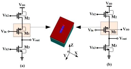
Figure 1.
Mixed-mode simulations of the degenerated common source (CS)-amplifier. The struck transistor M1 is modeled with (a) well and source tied together (bulk tied to source (BTS) configuration); (b) well tied to (normal configuration).
TCAD is adopted in this work to perform the device simulations. Typical P-substrate bulk CMOS technology is used in our simulations. The structural and doping profiles of the devices are calibrated to that of the 40 nm commercial SPICE models for DC and AC (transient) calibrations [19]. Transistor size, spacing, and well configuration are satisfied with the layout design rules. The size and bias of each transistor are set according to Table 1 to ensure that the device operates in the saturation region.

Table 1.
Size and bias of the transistors for simulation.
In the TCAD simulation process, a heavy ion strike is simulated as an electron-hole pair column with the track as its axis. Ion used in simulations has linear energy transfers (LETs) of 30 MeV·cm2/mg. The LET value is kept constant along the heavy ion track. The length and radius of the ion track are 10 µm and 0.025 µm, respectively. We simulated an ion strike at the center of the drain of the struck transistor normally. Similar to our previous works [20,21,22,23,24,25], the included physical models are: (a) Fermi–Dirac statistics, (b) the doping-dependent carrier mobility model with high electric field saturation, carrier–carrier scattering as well as interface scattering; (c) carrier recombination model: doping-dependent SRH and Auger recombination; (d) the effect of bandgap narrowing; (e) hydrodynamic carrier transport model; (f) and other models are configured with default models and parameters.
3. Simulation Results
In analog circuits, the transistors operate in a wide range of bias conditions, depending on the signal level at their inputs. The input and output characteristic of this circuit is simulated as shown in Figure 2. The simulated electric characteristics are almost similar in different well bias configurations. When the input voltage of the circuit is between 0.35 V and 0.55 V, the PMOS transistor works in the saturation region, and the amplifier works in the linear region.
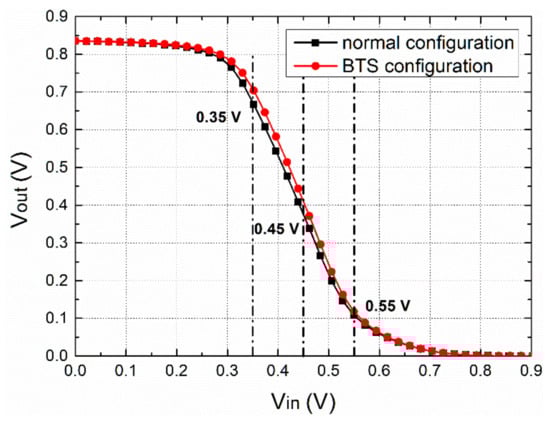
Figure 2.
Input and output characteristics of the CS amplifier.
Three input voltages (0.35 V, 0.45 V, and 0.55 V) are chosen to analyze the influence of input conditions on SETs. Striking location, angle of incidence, and other conditions are kept constant while the bias condition is changing.
Figure 3 illustrates the relationship between input conditions and transient voltage pulses obtained with different well bias configurations. Transient voltages produced in the two CS amplifiers show distinct distributions. For the struck transistor with well tied to the source, the amplitudes of transient voltage pulse are lower than those of the struck transistor with the well tied to . The high levels of transient voltage pulses remain constant with various input voltages since the state of M1 is driven to “on” as a result of charge generation after particle strike. Therefore, the peak voltage is determined by the charge collected by the device, M2 and M3 transistors, and the corresponding bias voltages and .
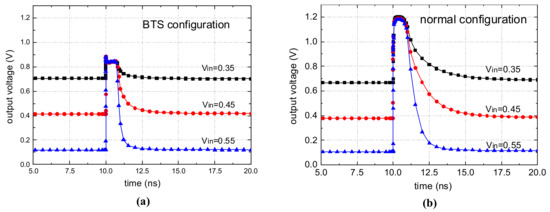
Figure 3.
Simulated transient voltages in three input conditions, (a) struck transistor with BTS configuration; (b) struck transistor with normal configuration.
SET mitigation comparison is outlined in Figure 4 when the input bias is 0.45 V. The black curve represents the SET of the normal circuit without any hardening technique. The red curve represents the SET shape when the well contact is tied to the source of the corresponding transistor. The circuit-adopted BTS configuration mitigates the amplitude of SET voltage pulse by 45%. For analog systems, only transients above a certain critical amplitude and longer than a certain critical duration are likely to cause system failure. For this work, we adopt a threshold of ±100 mV (the value chosen to represent the SET output for comparison of simulation results), which is the same as [26,27]. An event with a magnitude of over 100 mV (about 10% of full-scale) is sufficient to cause problems in most practical applications. The struck PMOS in normal configuration exhibits a much stronger transient, both in pulse duration and pulse amplitude. The simulation results show that the SET pulse width is 3.25 ns for the normal configuration and 1.22 ns for the BTS configuration with 100 mV of threshold voltage. The BTS technique reduces SET pulse width from the normal configuration over 62%.
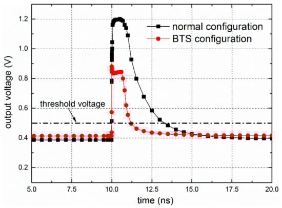
Figure 4.
Transient voltages at different well bias configurations.
4. Discussion
The physical mechanism of the BTS hardening technique can be explained from two aspects. First, the N-well potential influences SET amplitude. Figure 5 shows the electrostatic potential of a 1-D cut of the PMOS center structure perpendicular to the YoZ direction. In the bulk region (N-well region for PMOS), drain/well and source/well reverse-biased PN junctions exist along the source-channel-drain horizontal cutline before ion strike. After ion strike, the electric fields of the two PN junctions reduce but still exist in both well bias configurations. Even though an electronic barrier still remains, the resistance is lower after particle strike and the P+ drain potential tends to collapse to the N-well. Since the BTS configuration has a lower N-well potential, the SET amplitude is lower with the BTS configuration compared with the normal configuration after ion strike.
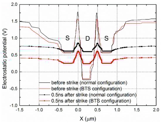
Figure 5.
A 1-D profile of the PMOS electrostatic potential distribution underneath surface 10 nm with different N-well bias configurations (the struck transistor is modeled in two fingers).
Second, the BTS hardening technique reduces the number of holes collected by the drain node. Resulting from the charge generation, M1 is “on” after ion strike. The drain and source collect holes while N-well collects electrons for the charge collection process in PMOS. Based on the charge conservation principle, the following must be satisfied:
, , and represent the charge collected by the drain, source, and N-well, respectively. With a decreasing well-biasing voltage in the BTS configuration, fewer electrons flow to the N-well after ion strike, which preserves more electrons recombine with holes, thus the holes collected by the drain and SET peak value are reduced in the BTS configuration.
SET pulse width is another important factor in identifying the single-event vulnerability, which is determined by the amount of charge collection and the rate of the charge restorability. When LET is large enough, SET pulse width () can be expressed as follows [28]:
where and are parameters related to device structure and is the saturated current of the pull-down NMOS. Neglecting the channel-length modulation effect, we assume is constant in the SET production process. It can be seen that the pulse width is proportional to the amount of charge collection . Since fewer holes are collected by the drain in the BTS configuration, the output ASET pulse width is narrower compared with normal configuration.
The function and performance of analog circuits are highly related to the precise design of the threshold voltage . Any factor causing the threshold shift must be considered. Body effect has the potential to shift the threshold voltage. For PMOS transistors, decreases as the N-well potential drops. Consequently, the electrical performance of the CS amplifier employed in the BTS RHBD technique will also be influenced. SPICE simulation is conducted for such a CS amplifier. The gain at 1K Hz is 10.143 dB and 10.638 dB for the normal and BTS configuration, respectively. The power consumption is 21.34 μW for the normal configuration and 22 μW for the BTS configuration. The simulation results from SPICE show that the BTS configuration has a negligible influence on circuit performance.
In this paper, the P-hit case serves as a simple example for the present study to analyze the effect of BTS hardening technique for ASET mitigation. The proposed BTS technique can be adopted in both PMOS and NMOS with the same physical mechanism. Note that, for NMOS adopting BTS configuration, a deep N-well implanted in the triple-well is needed to separate a P-well from common P-substrate.
5. Verification in Operational Amplifier Circuit
In order to evaluate the effectiveness of the SET mitigation technique in analog subsystem circuits, an operational amplifier circuit in a voltage follower configuration (unit gain) is designed and used for simulation. Operational amplifiers are wildly used in analog and mixed-signal circuits such as low drop-out (LDO) regulators, bandgap (BG) references, analog-to-digital converters (ADCs), digital-to-analog converters (DACs), comparators, and others.
Figure 6 presents the operational amplifier and the circuit configuration. The BTS hardening technique is adopted in M1 and M2 differential input transistors to evaluate the effectiveness of ASET mitigation. To ensure the correct operation of the design, functional verification is carried before the SET simulations. The simulation results of the open-loop circuit are shown in Figure 7, indicating that the circuit performances for the two well bias configurations are approximately equivalent. A gain-bandwidth (GBW) of 195 MHz and a phase margin (PM) of 70° are obtained for the operational amplifier. The 1 σ offset voltage of the process mismatch with 2 k points of Monte Carlo simulation is 6.7 mV for the normal configuration and 6.36 mV for the BTS configuration. These simulation results again indicate that a different N-well bias configuration has a negligible effect on the circuit performance.
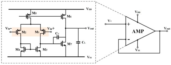
Figure 6.
Single-event transients (SET) simulation circuit consisting of an operational amplifier in voltage follower configuration (M1 and M2 modeled in BTS and normal configuration).
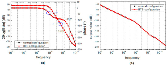
Figure 7.
Frequency response of the operational amplifier: (a) gain and phase; (b) output noise.
For the SET simulation, M1 is the struck transistor and modeled as the 3D TCAD model, while other devices use SPICE models. If there is a disturbance on the M1, the voltage of the operational amplifier will be influenced and thus the output of the voltage buffer will temporarily deviate from the input. The simulations are performed using mixed-mode TCAD simulations. A 525 mV DC input signal is applied to the input transmission gate.
Figure 8 demonstrates the effectiveness of the BTS hardening configuration. Heavy ion is injected in the test circuit at 50 ns with the same simulation methodology mentioned before. Due to the differential-mode amplification of the circuit, the output disturbance is evident. The peaking SET voltage is 518 mV for the normal voltage follower circuit, while it is 381 mV for the BTS RHBD circuit. In other words, BTS RHBD technique mitigates SET glitch by 26.4% of its original amplitude in this case. The SET pulse widths (the pulse width when the voltage is lower than 100 mV threshold voltage) are 6.2 ns for normal configuration and 1.5 ns for BTS configuration, respectively. The pulse width decreases by 75.8%.
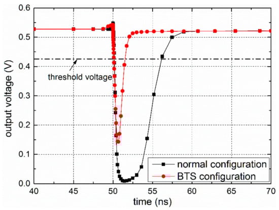
Figure 8.
SET induced voltage follower disturbance with different N-well bias configurations.
The characteristics of the proposed BTS technique are summarized and compared with other state-of-art techniques in Table 2. The BTS technique can be adopted freely in any circuits with stacked transistors. Comparing with other works, the advantages of the BTS are the negligible penalty and low design difficulty.
Table 2.
Comparison with other state-of-the-art analog single-event transient (ASET) mitigation methods.
6. Conclusions
In this paper, a technique tying bulk and source together (BTS configuration) for analog single-event transient mitigation is investigated. Based on commercial 40 nm bulk CMOS technology, the 3D TCAD simulation results indicate that the BTS configuration can mitigate SET pulse effectively with a negligible penalty. Detailed analyses show that the proposed BTS technique mainly affects the N-well potential. With an LET of 30 MeV·cm2/mg, the pulse width of the SET signal is reduced by 62% for single the CS amplifier and 75.8% for the voltage follower system. Without the performance penalty, this technique is universally applicable and provides new guidance for radiation-hardened analog circuit design.
Author Contributions
Conceptualization, J.L. and B.L.; methodology, J.C.; software, J.L.; validation, Y.C.; formal analysis, J.L.; investigation, J.L.; resources, B.L.; data curation, J.L.; writing—original draft preparation, J.L.; writing—review and editing, J.C.; visualization, Q.S.; supervision, Y.G.; project administration, Y.G.; funding acquisition, J.C. All authors have read and agreed to the published version of the manuscript.
Funding
This research was funded by the National Natural Science Foundation of China, grant number61974163.
Acknowledgments
Thanks for X.X.’s help in this work.
Conflicts of Interest
The authors declare no conflicts of interest.
References
- Wang, T. Study of Single-Event Transient Effects on Analog Circuits. Ph.D. Thesis, University of Saskatchewan, Saskatoon, SK, Canada, 2011. [Google Scholar]
- Zhao, Q.F.; Yang, G.Q.; Sun, Y.J.; Yu, P.F.; Chen, J.J.; Liang, B. Research on the effect of single-event transient of an on-chip linear voltage regulator fabricated on 130 nm commercial CMOS technology. Microelectron. Reliab. 2017, 73, 116–121. [Google Scholar] [CrossRef]
- Kessarinskiy, L.N.; Borisov, A.Y.; Boychenko, D.V.; Akhmetov, A.O. Electric regime influence on the DC-DC converters’s hardness to single event transients. Russ. Microelectron. 2015, 44, 44–48. [Google Scholar] [CrossRef]
- Andreou, C.M.; Javanainen, A.; Rominski, A.; Virtanen, A.; Liberali, V.; Calligaro, C.; Prokofiev, A.V.; Gerardin, S.; Bagatin, M.; Paccagnella, A. Single Event Transients and Pulse Quenching Effects in Bandgap Reference Topologies For Space Applications. IEEE Trans. Nucl. Sci. 2016, 63, 2950–2961. [Google Scholar] [CrossRef]
- Yuan, H.; Guo, Y.; Chen, J.J.; Chi, Y.Q.; Chen, X.; Liang, B. 28nm Fault-Tolerant Hardening-by-Design Frequency Divider for Reducing Soft Errors in Clock Data Recovery. IEEE Access 2019, 7, 47955–47961. [Google Scholar] [CrossRef]
- Yuan, H.Z.; Chen, J.J.; Liang, B.; Guo, Y. Fault-tolerant multi-node coupling triple mode redundancy voltage controlled oscillator for reducing soft error in clock and data recovery. Electron. Lett. 2019, 55, 250–252. [Google Scholar] [CrossRef]
- Atkinson, N.M.; Holman, W.T. The Quad-Path Hardening Technique for Switched-Capacitor Circuits. IEEE Trans. Nucl. Sci. 2013, 60, 4356–4361. [Google Scholar] [CrossRef]
- Armstrong, S.E.; Olson, B.D.; Holman, W.T.; Warner, J.; Mcmorrow, D.; Massengill, L.W. Demonstration of a Differential Layout Solution for Improved ASET Tolerance in CMOS A/MS Circuits. IEEE Trans. Nucl. Sci. 2010, 57, 3615–3619. [Google Scholar] [CrossRef]
- Hu, C.M.; Chen, S.M.; Chen, J.J.; Qin, J.R. The off-state gate isolation technique to improve ASET tolerance in differential analog design. Sci. China Technol. Sci. 2013, 56, 2599–2605. [Google Scholar] [CrossRef]
- Yang, Z.; Xie, X.; Fan, X.; Yang, Z.; Xie, X.; Fan, X.; Ren, Y. A novel single-event-hardened charge pump using cascode voltage switch logic gates. Microelectron. Reliab. 2018, 91, 269–277. [Google Scholar] [CrossRef]
- Loveless, T.D.; Massengill, L.W.; Bhuva, B.L.; Holman, W.T.; Witulski, A.F.; Boulghassoul, Y.A. Hardened-by-Design Technique for RF Digital Phase-Locked Loops. IEEE Trans. Nucl. Sci. 2006, 53, 3432–3438. [Google Scholar] [CrossRef]
- Qin, J.; Chen, S.; Guo, C.; Du, Y. Simulation Study of the Single-Event Effects Sensitivity in Nanoscale CMOS for Body-Biasing Circuits. IEEE Trans. Device Mater. Reliab. 2014, 14, 639–644. [Google Scholar]
- Harada, R.; Mitsuyama, Y.; Hashimoto, M.; Onoye, T. Neutron induced single event multiple transients with voltage scaling and body biasing. In Proceedings of the 2011 Reliability Physics Symposium (IRPS), Monterey, CA, USA, 10–14 April 2011. [Google Scholar]
- Razavi, B. Design of Analog CMOS Integrated Circuits; McGraw-Hill: Boston, MA, USA, 2001. [Google Scholar]
- Ruiqiang, S.; Shuming, C.; Yankang, D.; Pengcheng, H.; Jianjun, C.; Yaqing, C. PABAM, A Physics-Based Analytical Model to Estimate Bipolar Amplification Effect Induced Collected Charge at Circuit Level. IEEE Trans. Device Mater. Reliab. 2015, 15, 595–603. [Google Scholar] [CrossRef]
- Shuming, C.; Bin, L.; Biwei, L.; Zheng, L. Temperature Dependence of Digital SET Pulse Width in Bulk and SOI Technologies. IEEE Trans. Nucl. Sci. 2008, 55, 2914–2920. [Google Scholar] [CrossRef]
- Chen, J.; Chen, S.; He, Y.; Chi, Y.; Qin, J.; Liang, B.; Liu, B. Novel Layout Technique for N-Hit Single-Event Transient Mitigation via Source-Extension. IEEE Trans. Nucl. Sci. 2012, 59, 2859–2866. [Google Scholar] [CrossRef]
- Du, Y.; Chen, S.; Liu, B. A Constrained Layout Placement Approach to Enhance Pulse Quenching Effect in Large Combinational Circuits. IEEE Trans. Device Mater. Reliab. 2014, 14, 268–274. [Google Scholar] [CrossRef]
- Boulghassoul, Y.; Massengill, L.W.; Sternberg, A.L.; Pease, R.L.; Buchner, S.; Howard, W.; McMorrow, D.; Savage, M.W.; Poivey, C. Circuit Modeling of the LM124 operational amplifier for analog single-event transient analysis. IEEE Trans. Nucl. Sci. 2003, 49, 3090–3096. [Google Scholar] [CrossRef]
- Xu, J.; Guo, Y.; Song, R.; Liang, B.; Chi, Y. Supply Voltage and Temperature Dependence of Single-Event Transient in 28-nm FDSOI MOSFETs. Symmetry 2019, 11, 793. [Google Scholar] [CrossRef]
- Liang, B.; Song, R.; Han, J.; Chi, Y.; Chen, R.; Hu, C.; Chen, J.; Ma, Y.; Shangguan, S. Comparison of single-event upset generated by heavy ion and pulsed laser. Sci. China Inf. Sci. 2017, 60, 072401. [Google Scholar] [CrossRef]
- Huang, P.; Chen, S.; Chen, J.; Bin, L.; Wu, Z. Simulation study of large-scale charge sharing mitigation using seamless guard band. IEEE Trans. Device Mater. Reliab. 2016, 17, 176–183. [Google Scholar] [CrossRef]
- Huang, P.; Chen, S.; Chen, J.; Liang, B.; Song, R. The Separation Measurement of P-Hit and N-Hit Charge Sharing With an “S-Like” Inverter Chains Test Structure. IEEE Trans. Nucl. Sci. 2017, 64, 1029–1036. [Google Scholar] [CrossRef]
- Yu, J.T.; Chen, S.M.; Chen, J.J.; Huang, P. Simulation analysis of heavy-ion-induced single-event response for nanoscale bulk-Si FinFETs and conventional planar devices. Sci. China Inf. Sci. 2017, 60, 459–466. [Google Scholar] [CrossRef]
- Wu, Z.; Chen, S.; Yu, J.; Chen, J.; Huang, P.; Song, R. Recoil-ion-induced single event upsets in nanometer CMOS SRAM under low-energy proton radiation. IEEE Trans. Nucl. Sci. 2016, 64, 654–664. [Google Scholar] [CrossRef]
- Pease, R.L.; Sternberg, A.; Massengill, L.; Schrimpf, R.; Buchner, S.; Savage, M.; Titus, J.; Turflinger, T. Critical charge for single-event transients (SETs) in bipolar linear circuits. IEEE Trans. Nucl. Sci. 2001, 48, 1966–1972. [Google Scholar] [CrossRef]
- Adell, P.; Schrimpf, R.D.; Barnaby, H.J.; Marec, R.; Chatry, C.; Calvel, P.; Barillot, C.; Mion, O. Analysis of single-event transients in analog circuits. IEEE Trans. Nucl. Sci. 2001, 47, 2616–2623. [Google Scholar] [CrossRef]
- Chen, S.M.; Chen, J.J.; Chi, Y.Q.; Liu, F.Y.; He, Y.B. Modeling to predict the time evolution of negative bias temperature instability (NBTI) induced single event transient pulse broadening. Sci. China Technol. Sci. 2012, 55, 1101–1106. [Google Scholar] [CrossRef]
- Yuan, H.; Chen, J.J.; Liang, B.; Chi, Y.Q.; Chen, X.; Guo, Y. An SEU/SET-Tolerant Phase Frequency Detector With Double-Loop Self-Sampling Technology for Clock Data Recovery. IEEE Trans. Nucl. Sci. 2019, 66, 1483–1490. [Google Scholar]
© 2019 by the authors. Licensee MDPI, Basel, Switzerland. This article is an open access article distributed under the terms and conditions of the Creative Commons Attribution (CC BY) license (http://creativecommons.org/licenses/by/4.0/).